Note: Descriptions are shown in the official language in which they were submitted.
CA 02379896 2002-04-02
_1_
REFERENCE CELLS WITH INTEGRATION CAPACITOR
This application claims priority from Canadian Patent application 2,342,508
filed March 30,
2001.
FIELD OF THE INVENTION
The present invention relates to DKAM memories. More particularly the
invention relates to
bitline reference capacitors used in DRAM memories.
BACKGROUND OF THE INVENTION
Folded bitline DRAM architectures require a reference voltage on the
unaccessed bitline of a
complementary folded bitline pair in order to sense the voltage potential on
the accessed
bitline of a complementary folded bitline pair. Prior to a read operation from
the memory
cells, both bitlines of the complementary bitline pair are precharged to a mid-
point voltage
level. This mid-point voltage level is approximately a mid-point voltage
between the logic
"1" voltage potential level and the logic "0" voltage potential level, and can
be supplied by
voltage generators or through charge sharing by equalizing a pair of bitlines
carrying opposite
rail-to-rail voltage levels. During a read operation, a wordline is driven to
couple a DRAM
storage capacitor to one of the bitlines. If the storage capacitor stored a
logic "0" charge, then
the voltage level of the bitline it is coupled to will drop below the mid-
point voltage level. On
the other hand, if the storage capacitor stored a logic "1" charge, then the
voltage level of the
bitline will rise above the mid-point voltage level. The unaccessed bitline of
the
complementary bitline pair then serves as a reference voltage for the bitline
sense amplifier.
Unfortunately, the storage capacitor can only change the voltage level of the
precharged
bitline by a few hundred mini-volts, thus the sensing margin of the bitline
sense amplifiers is
small and susceptible to mis-reads.
Figure 1 is a diagram showing the relative bitline voltage levels during a
read access
operation for prior art DRAM devices. It is assumed that the DRAM memory cells
comprise
a p-channel access transistor and a planar storage capacitor, and the
unaccessed bitline BL is
used as the reference bitline in this example. The midpoint voltage level of
BL* is reduced
through capacitive charge sharing by a memory cell that stores a logical "0"
when a wordline
CA 02379896 2002-04-02
-2-
WL is driven to the low voltage level. Shortly thereafter, sense amplifier
enable signal SN
falls to the low logic level to activate the bitline sense amplifiers. The
bitline sense amplifiers
will detect that the voltage level of J3I,* is below the mid-point reference
voltage of BL and
subsequently drive BL* to ground and BL to VDD. The accessed memory cell
coupled to
BL* is then restored. Mis-reads firom the bitline sense amplifier will not
occur if the
necessary voltage difference 0v is maintained between the voltage level of the
accessed
bitline and the reference voltage oi'the unaccessed bitline.
However, DRAM memory cells exhibit asymmetrical leakage characteristics. More
specifically p-channel memory cells storing a logical "0" tend to leak towards
a logical "I"
value over time, while p-channel memory cells storing a logical "1" do not
leak much charge
over time. The dashed BL* line in Figure I illustrates the effect of coupling
a cell that stored
a logic "0" and has suffered leakage to BL*. Because the memory cell has
leaked towards the
logical "1" value, BL* is weakly pulled down to a valtage level above the
desired level
represented by the solid black line. Hence the voltage difference !!v is
reduced and data is
unpredictably read because the bitline sense amplifier will not be able to
differentiate
between the voltage levels of BL and BL*. Furthermore, the memory cell can
leak to a point
where the level of BL* is increased above the level of BL to cause a misread.
A known
solution for overcoming this problem is to use reference memory cells
connected to each
bitline. The reference memory cells, also known as dummy cells, are usually
identical to
normal memory cells in the memory array. The reference cells are commonly used
in full rail
bitline precharge schemes. Reference cells or dummy cells can be used to
adjust the reference
level if either "0" or "I" voltage levels cannot be fully restored. Tie use of
reference cells
increases the sense margin to compensate for leakage of the memory cells.
Reference cells
also provide improved noise immunity and faster sensing, for examp le.
Figure 2 is a general diagram of reference cells and an equalization
transistor. Each reference
cell has a p-channel access transistor with a source terniinal connected to a
bitline (not
shown) and a drain terminal coupled to a storage capacitor. One reference cell
has a gate
connected to a DWL_ ODD reference wordline signal and a drain terminal coupled
to storage
capacitor C1. The other reference cell has a. gate connected to a DWL EVEN
reference
wordline signal and a drain terminal coupled to storage capacitor C2. The
equalization
transistor is a p-channel transistor connected between the two storage
capacitors and having a
CA 02379896 2002-04-02
-3-
gate connected to an equalization signal EQ for shorting the two storage
capacitors together.
Although a common cell plate is shown as a dashed box that covers the areas of
C1 and C2,
those of skill in the art will understand that the cell plate extends to cover
all the storage
capacitor areas of the memory array.
In operation, both storage capacitors of the reference cells are initially
discharged upon power
up of the memory. During the first write operation, both the storage
capacitors will be
precharged to logic high and logic low levels, or logical "1" and "0" levels
and then
equalized to a mid-point voltage level. A dummy memory cell is then coupled to
the
unaccessed bitline of a complementary bitline pair during a sense operation
from an accessed
bitline. When a weak or leaked Io;gic "0" is read from the accessed bitline,
the voltage
difference between the two bitlines is sufficient for the bitline sense
amplifiers to latch the
data. After the data is fully latched lby the bitline sense amplifiers, the
reference cell of the
accessed bitline is turned on. Now both storage capacitars CI and C2 store
complementary
voltage levels. Therefore, when the wordlines are turned off and the
equalisation transistor is
turned on, charge is shared equally between C1 and C2 such that both their
voltage levels
should be at the mid-point voltage level. Although a p-channel equalisation
transistor is
shown, one skilled in the art should understand that an n-channE:l transistor
would work
equally well.
Although the use of reference cells in the at>ove mentioned application can
improve sense
margins for memory cells leaking s~:ored logical "0" levels, misreads can
still occur if the
reference cells themselves are not a~dequatel~~ charged to the mid-point
voltage level. This
problem occurs in high speed memory operations where the cycle time is too
short to allow
the reference cell to be fully restored prior to a subsequent operation, or if
the access
transistor wordline cannot be sufficiently boosted to pass the full voltage
level. This problem
also occurs if the restoration cycle is sufficiently different from the cycle
used to restore
sensed cells, and is more prevalent following write operations, as the write
operation is
typically shorter in duration than a read operation, leaving less time
available for restoring the
charges of the reference cells. The latter problem typically occurs in planar
memory cells that
utilize low voltage transistors. For e~;ample, one reference cell may not be
able to store full
logic "I" level while the other reference cell stores a full logic "0" level.
When equalized,
both reference cells will have stored a reference voltage less than the mid-
point voltage level.
CA 02379896 2002-04-02
-4-
This will degrade the capability of bitline sense amplifiers to accurately
read out data from an
accessed bitline, and in particular, from a leaking memory cell.
Therefore, there is a need for a reference cell equalisation circuit that
compensates for
reference cells that are unable to equalize to a mid-point voltage level for
reliable bitline
sensing operations. There is also a need for a reference cell arrangement that
allows for fast
equalisation of the reference cells for high ;peed operation using low leakage
connections
and minimized area. There is also a need for margin test capabilities through
access to the
reference cell voltage level.
SUMMARY OF TILE INVENTION
The object of the present invention is to mitigate or obviate at least one
disadvantage with
previous reference cells. In particular, it is an object of the present
invention to provide a
bitline reference circuit having an integration capacitor for compensating the
reference cell
storage capacitors such that their stored mid-point voltage levels are
adjusted towards the true
mid-point voltage level.
In a first aspect, the present invention provides a DRAM bitline reference
circuit that includes
a reference storage capacitor coupled to each bitline of a complementary pair
of bitlines. The
bitline reference circuit includes an integration capacitor for sharing charge
with the reference
storage capacitors, a precharge circuit for charging the integration capacitor
to a reference
voltage level, and an equalization circuit for coupling the integration
capacitor to the
reference storage capacitors.
In alternate embodiments of the present aspect, the reference storage
capacitors and the
integration capacitor are planar, p-channel capacitors. In yet another
embodiment of the
present aspect, the equalization circuit includes a p-channel transistor
having a source
terminal connected to the capacitor, a drain terminal connected to the
reference storage
capacitors, and a gate connected to an equalization signal. Alternatively, the
equalization
circuit includes a first p-channel transistor having a source terminal
connected to the
capacitor and a drain terminal connected to one of the reference storage
capacitors, and a
second p-channel transistor having a source terminal connected to the
capacitor and a drain
terminal connected to the other of the reference storage capacitors, and the
first and second p-
channel transistors have their gates connected to an equalization signal.
CA 02379896 2002-04-02
In a further embodiment of the present aspect, the precharge circuit includes
a p-channel
transistor for coupling a reference voltage to the integration capacitor in
response to a start-up
signal, where the reference voltage is the same as a bitline precharge
voltage.
In a second aspect, the invention provides a method for equalizing a first
reference memory
cell storage capacitor and a second reference memory cell storage capacitor
coupled to a
complementary pair of bitlines. The method includes precharging an integration
capacitor,
the first reference memory cell storage capacitor and the second reference
memory cell
storage capacitor to a reference voltage level, where the reference voltage
level is adjusted in
a test mode, driving the complementary pair of bitlines to complementary
voltage levels,
charging the first and second reference memory cell storage capacitors through
the
complementary pair of bitlines, and equalizing the first reference memory cell
storage
capacitor, the second reference memory cell storage capacitor and the
integration capacitor to
each other.
In an alternative embodiment of the present aspect, the integration capacitor
and the storage
capacitors are precharged during a power up phase. In an alternative
embodiment of the
present aspect, a wordline is activated to couple a memory cell storage
capacitor to one
bitline of the complementary pair of bitlines and a dummy wordline is
activated to couple the
first reference memory cell storage capacitor t:o the other bitline of the
complementary pair of
bitlines after precharging.
In yet another embodiment of the present aspect, the complementary pair of
bitlines are
driven to the complementary voltage levels by a bitline sense amplifier, and
another dummy
wordline is activated to couple the second reference memory cell storage
capacitor to the one
bitline of the complementary pair of bitlines.
In a third aspect, the present invention provides A DRAM bitline reference
circuit. The
bitline reference circuit includes a first reference cell having an access
transistor and a storage
capacitor, a second reference cell having an access transistor and a storage
capacitor, a bitline
coupled to the first reference cell, a complementary bitline coupled to the
second reference
cell, an integration capacitor, a precharge transistor for coupling a
reference voltage to the
integration capacitor, and an equalization circuit for coupling the
integration capacitor to the
storage capacitors of the first and second reference cells.
CA 02379896 2002-04-02
-G-
In an alternative embodiment of the present aspect, the equalization circuit
includes a first
transistor for coupling the integration capacitor to the storage capacitor of
the first reference
cell, and a second transistor for coupling the integration capacitor to the
storage capacitor of
the second reference cell.
In another embodiment of the present aspect; the access transistor late of the
first reference
cell is connected to a first dummy wordline, and the access transistor gate of
the second
reference cell is connected to a second dummy wordline. In yet another
embodiment of the
present aspect, the transistors are p-channel tr;~nsistors.
In a fourth aspect, the present invention provides A DRAM memory. The DRAM
memory
includes a DRAM bitline reference circuit having a reference storage capacitor
coupled to
each bitline of a complementary pair of bitlines, the bitline reference
circuit including an
integration capacitor for sharing charge with the reference storage;
capacitors, a precharge
circuit for charging the integration capacitor to a reference voltage level,
and an equalization
circuit for coupling the integration capacitor to the reference storage
capacitors.
BRIEF DESCRIPTION OF THE DRAWINGS
Embodiments of the present invention will now be described, by way of examples
only, with
reference to the attached Figures, wherein
Figure 1 is a diagram illustrating bitline voltages during a sensing operation
in prior
art DRAM devices;
Figure 2 is a general diagram of a reference cell equalisation circuit of the
prior art;
Figure 3 shows a layout of the reference cell precharge circuit according to
an
embodiment of the present invention;
Figure 4 shows a circuit schematic corresponding to the layout shown in Figure
3;
and,
Figure 5 is a sequence diagram illustrating bitline voltages during a sensing
operation
using the circuit of Figure 4.
CA 02379896 2002-04-02
_7_
DETAILED DESCRIPTION
A DRAM having integration capacitors coupled to dummy memory cells, also
referred to as
reference memory cells, of a folded bitline arrangement is disclosed herein.
The dummy
memory cells are substantially the same as normal memory cells, that are used
to provide
reference voltages representing the different logic states of the memory cells
and are not used
to store data. In a presently preferred embodiment, an integration capacitor
is coupled in
parallel to first and second dummy cells that store the voltages representing
logic "1" and
logic "0" respectively. In combination the two dummy cells provide a midpoint
voltage that
is achieved by equalising the voltage between the dummy memory cell having a
voltage
potential representing a logic "1" value, and the dummy memory cell having a
voltage
potential representing a logic "0" value using an equalisation transistor. The
integration
capacitor compensates for differences in logic "0" and "1" voltage levels to
ensure that the
reference cells are maintained at the proper mid-point voltage level after a
read operation.
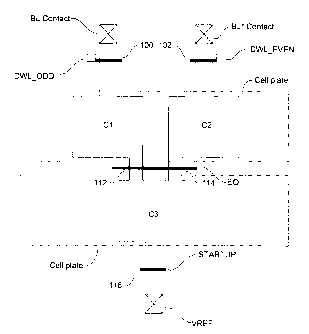
Figure 3 shows a layout of refer°ence cells and an integration
capacitor according to an
embodiment of the present invention. Full size reference cells, also referred
to as dummy
cells, are used in the presently preferred embodiment to make sensing
independent from
bitline precharge levels. This is useful for planar cell applications where
the wordline and
back bias boosting is limited, since low voltage transistors are used in this
embodiment.
Figure 3 includes access transistors 100 and 102 of respective reference cells
for coupling BL
and BL*, via bitline contacts, to storage capacitors C1 and C2 respectively.
An integration
capacitor C3 is coupled to both storage capacitors C1 and C2 through a pair of
p-channel
equalization transistors having their gates connected to equalization ignal
EQ. An additional
p-channel transistor having its gate connected to start-up signal STARTUP
couples C3 to a
bitline precharge voltage VREF. VREF is usually the same voltage used to
precharge the
bitlines to a mid-point voltage level, and is preferably at the 1/2VDD voltage
level. Without
negative boosting of wordlines, for e:Kample boosting of DWL ODI) and DWL
EVEN, it is
difficult to transfer a full charge from a bitline to the reference: storage
capacitor. The
reference cells and integration capacitor shown in Figure 3 are included in
each
complementary bitline pair in the memory array, and placed at either ends of
the
complementary bitline pairs. In general operation, signal STARTUP and EQ are
brought low
for precharging C1, C2 and C3 to the VREF level prior to any read operation,
such as in a
CA 02379896 2002-04-02
_g_
power up phase of the DRAM, for example. .After the first write and each
subsequent read or
write operation C1 and C2 will store complementary voltage levels, and EQ is
subsequently
brought low for coupling C1, C2 and C3 to each other. Although not shown in
Figure 3,
those of skill in the art would understand that a cell plate biased to a cell
plate voltage VCP
covers the storage capacitor active areas of all the memory cells.
Figure 4 shows a circuit schematic corresponding to the layout of the present
invention
shown in Figure 3. 'hhis layout is clearly only illustrative, and is not meant
to be limiting of
the scope of the present invention as one of skill in the art will readily
appreciate that
numerous modifications to the circuit can be made without departing from the
scope of the
present invention. Figure 4 shows a first reference cell having its storage
capacitor C1
coupled to bitline BL through access transistor 100, and a second reference
cell having its
storage capacitor C2 coupled to bitli.ne BL* through access transistor 102.
The first and the
second reference cell storage capacitors C 1 and C2 are coupled to integration
capacitor C3
through respective equalization transistors 112 and 114. Although the present
embodiment
illustrates the use of two equalization transistors, a single equalization
transistor having a
source terminal connected to C3 and a drain terminal connected to both C1 and
C2 can be
used in alternate embodiments. The cell plates of all the storage capacitors
are biased to a cell
plate voltage VCP. Dummy wordlines DWL ODD and DWL EVEN are connected to the
gates of access transistors 100 and 102 respectively, for coupling storage
capacitors Cl and
C2 to their respective bitlines. Integration capacitor C 1 is coupled to
bitline precharge
voltage VREF through precharge transistor 116. The complementary bitlines, BL
and BL*,
are also connected to a plurality o1° memory cells. For example, BL is
connected to memory
cell 108 through access transistor 104, while BL* is connected to memory cell
110 through
access transistor 106. Access transistor 104 is controlled by wordline WLO and
access
transistor 106 is controlled by WLI for coupling their respective storage
capacitors to BL
and BL*. Although not shown in Figure 4, the bulk terminal of each PMOS
transistor is
connected to a proper biasing voltage level, such as VPP for example.
A general read operation for illustrating the operation of the reference cell
circuits and the
integration capacitor are now described with reference to Figures ~l and S.
Figure 5 shows
graces for a wordline WLO, a complementary bitline pair BL,~BL* and bitline
sense amplifier
CA 02379896 2002-04-02
-9-
enable signal SN. The following example assumes that a logical "0" is stored
in memory cell
108.
In Figure 4 after powerup, both signals STARTUP and EQ are brought low to set
the initial
voltage on C1, C2 and C3 to VR>F,F. All the bitlines are precharged. to the
mid-point voltage
level of VREF and STARTUP is then forced high. EQ stays low until a row in the
memory
array is accessed. Prior to any word.lines being brought low, EQ is driven
high to turn off
equalization transistors 112 and 114.. In order to access the data stored in
memory cell 108,
WLO is brought to a low voltage, which turns on the access transistor 104. In
Figure 5, this
event is illustrated by WLO dropping to the low logic level. This results in
charge sharing
between the bitline and the storage capacitor of memory cell 108.
Consequently the voltage o:f BL drops slightly as illustrated in Figure 5. At
the same time that
WLO is brought low, DWL EVEN is brought low, which couples reference capacitor
C2 to
BL*. It is noted that prior to activation of WLO, the stored "0" in memory
cell 108 and the
mid-point voltage level initially set in storage; capacitors C1 and C2 are
leaking towards the
IS logical "1" level. The activation of the access transistor 102 results in
charge sharing between
BL* and the reference capacitor C'2 such 'that the voltage of BL* increases
slightly as
illustrated in Figure S. The sense amplifier is then activated by driving
signal SN in Figure S
to the low logic level, which then c:lrives BL and BL* to their full voltage
levels representing
logic "0" and "1" respectively. As thn~ access transistors 100 and 102 are
still turned on, these
full levels are written back into the reference cells. After the sense
amplifier has fully driven
the bitlines, DWL ODD is then brought low, which allows a full logic "0" level
to be written
into C1 while a full logic "1" level is written into C2. After the restore
operation is complete,
all wordlines and dummy wordlines are forced high, which turns off all the
access transistors.
'the EQ signal is then brought low and the charge stored on C1 and C2 is
averaged out across
C1, C2 and C3. Therefore, if either C',1 or C2 was not restored to a full
logic "0" or "1" level,
then averaging of the stored charge across C1, C2 and C;3 will compensate C1
and C2 such
that their stored mid-point voltage levels are adjusted towards the true mid-
point voltage
level. If memory cell 108 stored a logical "1" value, then the voltage level
of BL is increased
as illustrated in Figure S by the dashed line. Note that the charge sharing
between memory
cell 108 that stores a logical "1" value and BL will increase the voltage on
BL to a higher
CA 02379896 2002-04-02
- 10-
level than that induced on BL by its reference cell. The resulting voltage
level of BL is
typically about an order of magnitude: greater than the voltage level of BL*.
Conversely, to access the data stored in the other memory cell 11a, WL1 and
DWL ODD
are brought low. The data is read out onto the bitlines and the sense
amplifier is activated
which results in the bitlines being driven to their full levels. Then DWL EVEN
is activated
to write the full logic "1" value into storage capacitor C2. Then all
wordlines and dummy
wordlines are brought high and storal;e capacitors C1 and C2 are equalised.
As previously mentioned for a DRAM such as that shown in Figure 4, a stored
logical "1"
value will tend not to leak away. I-lowever, a. stored "0" will tend to leak
towards the value
"1" as will the stored mid-point value. For reasons well known in the art, the
"0" will leak at
a faster rate than the midpoint voltage. if the array is not accessed for a
period of time all the
stored "0" levels will tend to move towards the "1" value. Thus the; mid-point
stored on C1
and C2, which is an average of the voltages of a logical "1" and a logical "0"
will also move
towards the "1" value. When the array is subsequently accessed, the reference
cell will induce
a slightly higher voltage on its bitline which should be representative of the
average voltage
of the data. The accessed memory cell will couple its storage capacitor to its
bitline, and the
bitline sense amplifier will operate on the accessed bitline voltage level and
the reference
voltage level of the unaccessed bitline. As rows are subsequently accessed,
the value stored
on the integration capacitor will move towards the true midpoint, reflecting
the fact that the
data has been recently accessed.
By using integration capacitor C3, the reference level stored in the reference
cells is adjusted
to
y - (vo+vl)c+(v~~.~ XC3)
2C+C3
where V0, V1, and V'a,,e represent lhe; voltages associated with logic "0",
logic "1", and their
average respectively. The charge Q~R=VR*(_' will be introduced into reference
BL during
activation. Capacitor C3 compensates for "'0" and "1" differencc;s during
various access
cycles.
In alternative embodiments of the present invention, the size of capacitor C1
can be adjusted
to allow control over the degree of integration desired, and is preferably at
least the same size
as capacitors C1 and C2. Although the degree of integration increases as the
size of capacitor
CA 02379896 2002-04-02
-11-
C1 increases, its size is limited by the area or space available between
complementary
bitlines. The precharge signal STA12TUP can be pulsed to additionally
compensate for an
offset, either connecting momentarily to VRIE:F or to other another reference
voltage VREF.
This could be done based on the information stored in a dummy column. Such
system could
compensate for the leakage associated with refreshing the individu~rl rows.
Furthermore, the
embodiments of the present invention are not limited to DRAM cells having
planar storage
capacitors, but are also applicable: to DRAM cells having trench or stacked
storage
capacitors. VREF can be adjusted in a test mode to determine: the optimum
level for
customized memory arrays.
In yet another alternative embodiment of 'the present invention, an additional
reference
column can be added to modify the reference cell action through either timing
or offset in the
sense amplifier action, or in other ways, known to one of skill in the art, to
compensate for
the elapsed time difference between the reference cell restore and sensed cell
restore
operation.
I S The above-described embodiments of the invention are intended to be
examples of the
present invention. Alterations, mc7difications and variations may be effected
the particular
embodiments by those of skill in the art, without departing from the scope of
the invention
which is defined solely by the claims appended hereto.