Note: Descriptions are shown in the official language in which they were submitted.
CA 02381167 2002-02-06
WO 01/10014 PCT/USOO/20092
INTERMODULATION PRODUCT CANCELLATION CIRCUIT
BACKGROUND OF THE INVENTION
The present invention relates to the reduction of distortion in electrical
circuitry. More particularly, the present
invention relates to distortion reduction circuitry particularly suitable for
amplifiers.
Radio frequency (RF) systems, such as cellular and microwave communication
systems, typically require input signals
to be fed into an RF power amplifier. Unfortunately, all amplifiers tend to
distort the input signal at some power level and to
generally cause the amplifier output to contain undesirable distortion
products, spurious products, noise perturbations and
intermodulation (IM) products. For purposes of simplicity, these will
collectively be referred to as IM products. These IM
products can cause undesirable interference over the amplifier frequency
range. It is for these reasons that most amplifiers
must incorporate some form of correction mechanism into the signal flow path
through the amplifier.
One conventional method for reducing IM products uses a spectral analysis
approach. This approach involves
scanning the output of the amplifier using a receiver tuned to the frequency
of candidate IM products. The IM level is measured
and a linearizer is manually adjusted to minimize the IM product. This
procedure is repeated until each of the IM products have
a magnitude below a predetermined acceptable level. In a similar approach, as
described in U.S. Patent No. 4,580,105 issued
to Myer, a portion of the output signal is taken and combined with an input
signal which has been adjusted in phase and
amplitude. The signal combination isolates the distortion component which is
then adjusted in phase and gain. This isolation
distortion component is then added back to the output signal by means of a
coupler to eliminate the distortion component.
Unfortunately, the amount of distortion reduction available using this feed
forward technique is limited by the accuracy of the
gain and phase adjustments.
In addition, there appears to be a problem in the number of samples realized
in several basic feed forward techniques.
Samples in these systems are available only at the time that the phase
detector circuit detects a correlated signal. This leads
to poor error signal resolution and it is this error signal that is used to
cancel corresponding spurs.
Moreover, it is believed that many cellular communication base stations do not
function at full capacity because of
serious linearity problems in the base station's components. In addition, the
need for increased capacity accompanying the
expansion of cellular communications is forcing requirements for transmission
standards of RF equipment to become too
stringent to be met by construction of most present day amplifier circuits.
Moreover, both time division multiple access (TDMA)
and code division multiple access (CDMA) modulation require greater linearity
and an absence of IM products that can not be
routinely obtained by presently available high efficiency RF power amplifiers.
Accordingly, it is clear that present correction
techniques for eliminating IM products are not acceptable for evolving
communications systems.
Thus, there is a need for a cancellation circuit which reduces IM products in
electronic circuitry such as power
CA 02381167 2009-02-20
amplifiers.
It would also be highly advantageous if the IM cancellation circuit were
inexpensive to manufacture and highly
reliable.
Moreover, it would be highly advantageous if the IM cancellation could be
provided in a compact and lightweight
constriction.
SUMMARY OF THE INVENTION
Briefly, in accordance with the invention, I provide an improved apparatus and
method for automatically reducing
IM products in electrical circuits: It is believed that this IM cancellation
circuit is particularly suitable for application with
amplifiers which amplify an input carrier signal.
Accordingly, in one aspect of the present invention there is provided an
intermodulation (IM) product cancellation
circuit for reducing one or more IM products in a carrier signal, the IM
product cancellation circuit comprising:
a variable oscillator for producing an IM product cancellation signal;
a variable phase shifter means for shifting said IM product cancellation
signal 1800 with respect to an IM product in
a carrier signal for canceling an unwanted IM product in the carrier signal;
a processor connected to said variable oscillator and said variable phase
shifter for controlling said variable
oscillator and said variable phase shifter means for initiating and
maintaining said IM product cancellation signal at
substantially the same frequency as the IM product but shifted 180 with
respect to the IM product for substantially reducing
an unwanted IM product in the carrier signal; and
a coupler means for combining the carrier signal with said IM product
cancellation signal to produce an output signal
having the IM product being substantially reduced.
According to another aspect of the present invention there is provided a
method of canceling unwanted IM products
in a carrier signal comprising the steps of:
sampling the carrier signal to produce a carrier signal sample;
analyzing the carrier signal sample to determine if the carrier signal has an
unwanted IM product;
analyzing the carrier signal sample to determine if the carrier signal has an
unwanted IM product;
controlling a variable oscillator to produce an IM product cancellation signal
having substantially the same frequency
as the unwanted IM product;
shifting the IM product cancellation signal 180 with respect to the IM
product in the carrier signal; and
combining the carrier signal with the IM product cancellation signal to
produce an output signal with the unwanted
IM product being substantially canceled by the IM product cancellation signal.
2
CA 02381167 2009-02-20
In its most basic form, the IM product cancellation circuit includes a first
coupler for sampling an input carrier signal.
The coupler isolates a portion of the signal, preferably 6 dB below the input
carrier signal so as to not substantially affect the
energy level of the input carrier signal. This sample signal is then routed to
a stepping spectrum analyzer which detects and
measures the frequency and amplitude of the signal components of the carrier
signal including its intended components and
any IM products in the carrier signal. The stepping spectrum analyzer
transmits the information relating to the frequency and
amplitude of the different signal components in the carrier signal to a
processor. Meanwhile, the processor stores information
relating to the identity of the amplitude and/or frequency or frequency bands
of intended signal components in the carrier signal.
This information is typically in the form of look-up tables which identifies
the amplitude or frequency, or in the case of TDMA
or CDMA systems, the frequency band where the intended signal components are
expected to reside. In this manner, the
processor, by referencing this look-up table, can determine whether the signal
components detected and measured by the
stepping spectrum analyzer are intended signal components or unintended IM
products.
The IM product canceling circuit further includes a variable voltage
controlled oscillator, variable amplifier and variable
phase shifter. The voltage controlled oscillator, amplifier and phase shifter
are connected in series for creating an oscillator
signal which can be controlled in amplitude and phase. The operation of the
voltage controlled oscillator, amplifier and phase
shifter are all controlled by the processor. Upon recognition and measurement
of an IM product by the stepping spectrum
analyzer and processor, the processor controls the voltage controlled
oscillator, amplifier and phase shifter to produce an
oscillating signal which is substantially identical in amplitude and frequency
to a detected IM product but shifted in phase by
180 . This oscillating signal acts as an IM cancellation signal as the signal
is fed back into the original carrier signal by means
of a coupler or the like, such as a combiner. The original carrier signal is
then output from the coupler retaining all of the original
characteristics of the intended signal components except that the unintended
IM product is canceled by the cancellation signal.
In a preferred embodiment, the IM cancellation circuit includes a feedback
circuit. After the IM product is canceled,
2a
CA 02381167 2002-02-06
WO 01/10014 PCT/US00/20092
the output carrier signal is sampled by splitting the output signal with a
coupler or the like to produce a sample of the output
carrier signal. This sample of the output carrier signal is routed back to, in
turn, the stepping spectrum analyzer and processor.
The stepping spectrum analyzer and processor are thus able to confirm that the
IM product has been canceled. In the
alternative, where it has been determined that the cancellation signal is
being transmitted at an incorrect frequency, amplitude
or phase, the voltage controlled oscillator, amplifier and phase shifter are
automatically adjusted by the processor until the
cancellation signal correctly cancels the unintended IM product.
As would be understood by those skilled in the art, the aforementioned
described cancellation circuit would only
cancel a single unintended IM product. Where the carrier signal is likely to
have more than one unintended IM product, the
cancellation circuit is provided with a plurality of variable voltage
controlled oscillators, variable amplifiers and variable phase
shifters. Each set of these voltage controlled oscillators, amplifiers and
phase shifters are connected in series to the processor
for creating a plurality of cancellation signals where necessary.
In an additional preferred embodiment, the IM product cancellation signal is
adapted for use with an amplifier. A
portion of the output from the amplifier is forwarded to the stepping spectrum
analyzer for recognition and measurement of
not only the intended signal components but also any IM products. This
information is sent to the processor which determines
whether the signals received by the stepping spectrum analyzer are intended
signal components or unintended IM products.
Whether the carrier signal includes IM products can be determined by
comparison of the received signals to look-up tables
which identify the amplitude and/or frequency band of the intended signal
components. If a detected signal is not listed in the
look-up table, the signal is recognized as an IM product.
In an additional embodiment, the amplifier input signal is split with a first
component going to the amplifier and a
second component, typically 6 DB below the signal input to the amplifier,
being sent to the stepping spectrum analyzer for
analysis. The frequencies of signals originally input in the amplifier are
identified as intended signal components and stored
in the processor. The frequencies of the intended signal components are then
compared with the frequencies of signals output
from the amplifier. IM products can then be identified as appearing at
frequencies not appearing in the amplifier input signal.
The processor then controls the variable voltage controlled oscillator and
variable amplifier to produce a cancellation signal
having a frequency and amplitude substantially equal to the frequency and
amplitude of the IM product. The cancellation signal
is then shifted in phase 180 with respect to the phase of the IM product and
combined with the carrier signal by means of a
coupler or the like. The resulting carrier signal is thus "cleansed" with the
IM product removed.
In still an additional preferred embodiment, the amplifier circuit includes a
traditional feed forward correction circuit.
The feed forward correction circuit will typically cancel much of the noise
and IM products of an amplifier. However, the
components of the feed forward correction circuit, such as combiners,
amplifiers and phase shifters, etc., typically add
additional IM products to the amplifier output. These IM products can be
canceled by application of the IM cancellation circuit
3
CA 02381167 2009-02-20
of the present invention. As described above, the output signal from the
amplifier is split with a component going to the
stepping spectrum analyzer. IM products are then recognized by the processor
by use of a look-up table or by comparison to
an analysis of the original amplifier input signal. The processor then
controls the variable controlled oscillator, variable amplifier
and variable phase shifter to produce a cancellation signal substantially
equal in frequency and amplitude to the IM product but
shifted in phase by 180 . This cancellation signal is then combined with the
amplifier output sig nal to cancel the unintended
IM product.
A preferred embodiment of the stepping spectrum analyzer for use in
application with the present invention is
substantially similar to the automated. frequency stepping noise measurement
test system disclosed and described in U.S.
Patent No. 6,393,272, "Automated Frequency Stepping Noise Measurement System".
In a preferred embodiment, the stepping
spectrum analyzer includes a variable low noise source for producing a low
noise signal having an adjustable frequency. The
variable low noise source includes two outputs for outputting identical low
noise signals, or is coupled to a splitter for splitting
a low noise signal into two identical low noise signals. The first low noise
signal is routed to a coupler which combines the
first low noise signal with that portion of the input carrier signal
comprising the sample signal. The second low noise signal
is routed to a variable phase shifter which adjust the phase of the second low
noise signal to be 90 out of phase (in phase
quadrature) with respect to the first low signal which has been combined with
the sample signal. The sample signal, carrying
the intended carrier signal components and any unintended IM products, and the
first low noise signal are then sent together
to a mixer where the signal is mixed with the second low noise signal which
has been adjusted in phase. Due to the inherent
characteristics of a mixer, the low noise source signals are canceled in the
mixer output signal by having the second low noise
signal shifted in phase 90 with respect to the first low noise signal.
Moreover, the mixer is nonlinear producing an output
signal including only a single sideband with respect to the frequency of the
low noise signal but having double the amplitude.
The signal output from the mixer, hereinafter referred to as a "measurement
test signal", is then sent to a variable low noise
matching amplifier. The variable low noise matching amplifier both amplifies
the measurement test signal and acts as a buffer.
The matching variable amplifier is constructed to add very low noise or IM
products so as to not interfere with the IM
measurements by the stepping spectrum analyzer and provides for amplification
of the measurement test signal to enhance the
ability of the stepping spectrum analyzer to measure any IM products in the
original sample signal.
After passing through the low noise matching amplifier, the measurement test
signal is sent to an analog-to-digital
convertor (ADC) which converts the analog measurement test signal into digital
data. The digital data is then transmitted to
a processor for evaluation. The processor of the stepping spectrum analyzer
may be separate and independent from the
processor which controls the variable voltage controlled oscillator, variable
amplifier and phase shifter which creates the IM
product cancellation signal, or both processor functions may be combined in a
single processor. The processor of the stepping
spectrum analyzer uses standard, windowed, fast or discreet fourier transforms
to accurately measure the characteristics of
4
CA 02381167 2002-02-06
WO 01/10014 PCTIUSOO/20092
the measurement test signal and whether it includes any IM products. These
fourier transforms are known to those skilled in
the art and will not be discussed in detail herein.
The processor of the stepping spectrum analyzer is connected to a plurality of
control lines to the variable amplifier,
variable low noise source, variable phase shifter and variable low noise
matching amplifier. These control connections enable
the processor to automatically set levels and make adjustments to the
amplifier, low noise source, phase shifter and matching
amplifier to "step" the low noise source across a desired frequency band at
different offset frequencies in order to identify the
IM products in that frequency band. To control the stepping spectrum analyzer,
the processor takes the digitized output from
the ADC to both calibrate the system and to ensure that the amplifier, low
noise source and phase shifter are set to correct
levels. More particularly, the output from the ADC enables the processor to
determine whether the low noise source is providing
the first and second low noise signals at a correct frequency. By evaluating
the output from the ADC, the processor can also
confirm that the phase shifters are properly maintaining the signals received
by the mixer in phase quadrature. If any of these
components are not functioning optimally, the processor automatically makes
required adjustments to ensure proper recognition
and measurement of any IM products in the carrier signal. Once the frequency
characteristics are recognized and measured
by the stepping spectrum analyzer, this signal information is sent to the
processor which controls the variable voltage controlled
oscillator, variable amplifier and variable phase shifter which produce the
cancellation signal. This processor (by comparison
of the signal information to internal lookup tables) determines whether the
carrier signal is carrying any unintended IM products
and controls the variable controlled oscillator, variable amplifier and
variable phase shifter to produce a cancellation signal which
is combined with the carrier signal to cancel an unintended IM product.
It is thus an object of the present invention to provide an improved apparatus
and method for canceling IM products
in electronic circuitry.
It is an additional object of the present invention to provide an IM
cancellation circuit which is inexpensive to
manufacture, highly reliable, compact and of lightweight construction.
These and other further advantages of the present invention will be
appreciated by those skilled in the art upon
reading the following detailed description with reference to the attached
drawings.
BRIEF DESCRIPTION OF THE DRAWINGS
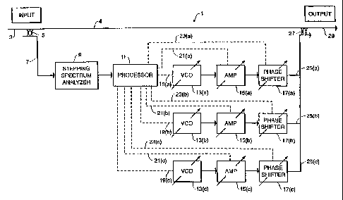
Fig. 1 is a diagram showing a simplified IM product cancellation circuit of
the present invention;
Fig. 2 is a diagram showing the IM product cancellation circuit of the present
invention including a feedback circuit;
Fig. 3 is a diagram illustrating the IM product cancellation circuit of the
present invention including a plurality of
variable voltage controlled oscillators, variable amplifiers and variable
phase shifters for producing a plurality of IM product
cancellation signals;
CA 02381167 2002-02-06
WO 01/10014 PCT/USOO/20092
Fig. 4 is a diagram illustrating a preferred embodiment of the stepping
spectrum analyzer utilized by the IM product
cancellation circuit of the present invention;
Fig. 5 is a diagram illustrating an amplifier circuit incorporating a
traditional feed forward correction circuit and an
IM product cancellation circuit of the present invention;
Fig. 6 is a graphical depiction, as would be shown on the display of a
traditional spectrum analyzer, illustrating a
carrier signal carrying both an intended signal and an unintended IM product;
and
Fig. 7 is a graphical depiction, as would be shown on the display of a
traditional spectrum analyzer, illustrating the
carrier signal shown in Fig. 6 with the IM product being substantially
canceled by application of the IM product cancellation
circuit of the present invention.
DETAILED DESCRIPTION OF THE INVENTION
While the present invention is susceptible of embodiment in various forms,
there is shown in the drawings and will
hereinafter be described the presently preferred embodiments of the invention
with the understanding that the present
disclosure is to be considered as an exemplification of the invention and is
not intended to limit the invention to the specific
embodiments illustrated.
With reference to Figs. 1 & 6, the IM product cancellation circuit 1 of the
present invention includes a stepping
spectrum analyzer 9, a processor 11, a variable voltage controlled oscillator
13, variable amplifier 15 and variable phase shifter
17. A carrier signal 4 which is intended to have its IM products canceled is
received by an input 3. The carrier signal is then
split by a coupler 5 with a portion, typically 6 dB below the input carrier
signal, being sent to the stepping spectrum analyzer
9. The signal sent to the stepping spectrum analyzer 9, hereinafter referred
to as a sample signal 7, is analyzed by the stepping
spectrum analyzer 9 for detection and measurement of the frequency and
amplitude of signal components in the input carrier
signal. These signal components which comprise the carrier signal 4 include
both intended signal components 91 and any
unintended IM products 93 (See Fig. 6). Once the stepping spectrum analyzer 9
has stepped across a frequency band of interest
and recognized the frequency and amplitude of the different signal components
of the carrier input signal within that frequency
band, this information is sent to the processor 11.
The processor 11 stores information relating to the identity of the frequency
and/or frequency bands within which
the intended signal or signals are expected to reside within the carrier input
signal. This information relating to the intended
signal components is typically stored in the form of look-up tables which
identifies the amplitude or frequency or frequency band
where the intended signal components of the carrier input signal 4 are
intended to be located within. The processor 11, by
cross referencing the information provided by the stepping spectrum analyzer 9
relating to recognized signals in the carrier input
signal 4 with the information stored in the look-up table, can determine
whether there are any unintended IM products within
6
CA 02381167 2002-02-06
WO 01/10014 PCTIUSOO/20092
the carrier input signal 4. Simply, any signal components identified by the
stepping spectrum analyzer 9 which are not listed
by amplitude frequency in the processor look-up table are determined to be IM
products 93.
The IM product cancellation circuit 1 of the present invention further
includes a plurality of control lines 19, 21 and
23 which connect the processor 11 with the variable voltage controlled
oscillator 13, variable amplifier 15 and variable phase
shifter 17, respectively. By means of these control lines 19, 21 and 23, the
processor 11 instructs the variable voltage
controlled oscillator 13 and variable amplifier 15 to create an oscillating
signal which is identical in frequency and amplitude
to a detected unintended IM product. This oscillating signal acts as a
cancellation signal 25 which is adjusted in phase by the
variable phase shifter 17 to be 180 with respect to the phase of the IM
product in the carrier input signal 4. With reference
also to Fig. 7, the cancellation signal 25 is then combined with the original
carrier input signal 4 by a second coupler 27 or the
like to create an output signal 29. As would be understood by those skilled in
the art, the output signal 29 is identical to the
original carrier input signal 4, retaining all of its original frequency and
amplitude characteristics of the intended signal
components 91, except that the unintended IM product 93 has been canceled by
the cancellation signal 25.
With reference to Fig. 2, in a preferred embodiment, the IM product
cancellation signal 1 includes an additional
feedback circuit which includes a third coupler 31 creating a feedback signal
33. After the IM product is canceled by combining
the cancellation signal 25 with the carrier input signal 4, the resulting
output signal 29 is split by a coupler 31 or the like which
isolates a portion of the output signal 29, again preferably 6 dB below the
output signal 29 so as to create feedback signal 33.
The feedback signal 33 is then routed back to the stepping spectrum analyzer 9
wherein it is analyzed across the desired
frequency band to confirm that the previously detected IM product has been
properly canceled. Where the IM product has not
been properly canceled, the processor 11 can adjust the variable voltage
controlled oscillator 13, variable amplifier 15 and/or
variable phase shifter 17 to ensure that the cancellation signal 25 has the
proper frequency, amplitude and phase shift to
properly cancel the IM product in the carrier input signal 4.
The previously described IM product cancellation circuit 1 is only capable of
canceling a single unintended IM product.
With reference to Fig. 3, in a preferred embodiment, the cancellation circuit
25 includes a plurality of variable voltage controlled
oscillators 13a - c, variable amplifiers 15a - c and variable phase shifters
17a - c. Each set of variable voltage controlled
oscillators 13a - c, variable amplifiers 15a - c and phase shifters 17a - c
are connected in series and connected to the processor
11 by control lines 1 9a - c, 21 a - c and 23a - c for enabling the processor
11 to create a plurality of controllable oscillating
signals which can be adjusted in amplitude by the variable amplifiers 15a - c
and phase by the variable phase shifters 17a - c.
For example, Fig. 3 shows three (3) sets of variable controlled oscillators
13a - c, variable amplifiers 15a - c and variable phase
shifters 1 7a - c which are capable of producing three (3) cancellation
signals 25a - c. Where the stepping spectrum analyzer
9 and processor 11 have measured and recognized three (3) IM products, the
variable voltage controlled oscillators 13a - c and
variable amplifier 15a - c are adjusted to produce three (3) cancellation
signals 25a - c having the same frequency and amplitude
7
CA 02381167 2002-02-06
WO 01/10014 PCTIUSOO/20092
as the three IM products recognized by the stepping spectrum analyzer 9 and
processor 11. These cancellation signals 25a
- c are then individually shifted in phase by phase shifters 17a - c so that
they are each shifted 180 with respect to the IM
product with which they are intended to cancel. Each of these cancellation
signals 25a - c are then coupled back to the carrier
input signal 4 to create an output signal 29. Again, the output signal 29
includes all of the signal characteristics of the carrier
input signal 4 except that the three (3) detected IM products have now been
canceled.
The IM product cancellation circuit 1 of the present invention is believed to
be particularly applicable to the
cancellation of IM products in amplifiers. Typically, amplifiers use some sort
of feed forward correction circuit (FFCC) in an
effort to cancel the IM products created by an amplifier. Unfortunately,
though a feed forward correction circuit often
substantially cancels the IM products of the amplifier itself, the feed
forward correction circuit introduces additional IM
products as a result of the additional components of the feed forward
correction circuit, such as phase shifters, variable
amplifiers and combiners. These IM products are then output as part of the
amplifier output signal. With reference to Fig. 5,
the IM product cancellation circuit 1 of the present invention can be used to
cancel the IM products of a feed forward correction
circuit 67 employed to cancel the IM products of a primary amplifier 77. For
purposes herein, the term "primary amplifier" is
intended to be used in the broadest sense to include any amplitifers, such as
RF amplifiers, IF amplifiers, power amplifiers, etc.
A primary amplifier 77 employing a feed forward correction circuit 67
typically includes additional phase shifters 75 and 83,
a variable amplifier 81 and combiners 79 and 85. An input signal 69 is split
by a coupler 71 with a first portion of the input
signal 69 being shifted 90 by phase shifter 75 and sent to a combiner 79. The
predominant portion of the input signal 69 is
routed to the primary amplifier 77 and amplified accordingly. A portion of
this amplified signal, including any IM products, is
isolated by an additional coupler 72 and also sent to combiner 79. The portion
of the amplified signal which is sent to the
combiner 79 is combined with the phase shifted input signal 73 in the combiner
79 which results in a first combiner output
signal 80. The original signal components of signal 69 are substantially
canceled and instead the first combiner output signal
80 includes only the IM products of the amplifier 77. Meanwhile, the amplifier
output signal is phase shifted by 180 by the
second phase shifter 83 and sent to a second combiner 85. This phase shifted
amplifier signal is mixed with the first combiner
output, which includes only the IM products created by the amplifier. This
first combiner output is adjusted in amplification
by amplifier 81 to have substantially the same amplitude as the IM products of
the amplifier output signal. Because the
amplifier output signal has been phase shifted by 180 by the phase shifter
83, the IM products of the primary amplifier are
substantially canceled in output carrier signal 4.
With reference to Figs. 1, 5, 6 & 7, in order to cancel the additional IM
products created by the components of feed
forward correction circuit 67, the carrier signal 4, output by the feed
forward correction circuit, is split by a coupler 5 with
a portion of the output signal 7 being sent to the stepping spectrum analyzer
9. The stepping spectrum analyzer 9 steps across
a desired frequency band in an effort to recognize the intended signal
components 91 and unintended IM products 93 of the
8
CA 02381167 2009-02-20
carrier signal 4. In similar manner to as described above, the stepping
spectrum analyzer 9 forwards the information regarding
the frequency and amplitude of the different signals that were recognized in
the carrier signal 4 to the processor 11 which cross
references this information with an internal lookup table which stores
information regarding the frequency of the intended
output signals of the amplifier 77. Any signals uncovered by the stepping
spectrum analyzer 9 which are not listed in this
internal look-up table are thus determined to be unintended IM products. Upon
recognition of these unintended IM products
93, the processor 11 controls the variable voltage controlled oscillator 13
and variable amplifier 15 to create a cancellation
signal 25. The phase shifter 17 then shifts the phase of the cancellation
signal 25 by 180 with respect to the IM products
of the carrier signal 4 and the cancellation signal 25 is thereafter combined
back with the carrier signal 4 to create an output
signal 29. Because the cancellation signal 25 has the same frequency and
amplitude as the IM products 93 but a shift of phase
of 180 , the output signal 29 includes all of the frequency and amplitude
characteristics of the intended signal components 91
of the signal created by the amplifier 77 but the unintended IM products 93
have been canceled.
With reference to Fig. 5, in an additional preferred embodiment, prior to the
input signal 69 being received by the
amplifier 77 or the feed forward correction circuit 67, the input signal 69 is
split by a coupler (not shown) for isolating a portion
of the input signal (not shown). This portion of the input signal is then
forwarded to the stepping spectrum analyzer 9 for
analysis which forwards the results, including determination of frequency and
amplitude components of input signal 69, to the
processor 11 which stores this information in look-up tables or the like to
provide the processor 11 with information relating
to the intended frequency and amplitude characteristics of the input signal
69. Since this information does not include any of
the IM products created by the amplifier 77 or feed forward correction circuit
67, the sample signal 7 can be compared with
the information now stored in the look-up table to identify the IM products of
the carrier signal 4 which were created by the
amplifier 77 or feed forward correction circuit 67. This information can, in
turn, be used to control the variable voltage
controlled oscillator 13, variable amplifier 15 and variable phase shifter 17
to create a cancellation signal 25.
As would be understood by those skilled in the art, it is important that the
stepping spectrum analyzer 9 quickly and
thoroughly analyze a frequency band of interest to determine the frequency and
amplitude of the different signal components
of a carrier signal, particularly any unintended IM products. Referring to
Fig. 4, a preferred stepping spectrum analyzer 9
includes a variable low noise source 37, variable phase shifter 43 and mixer
47. The variable low noise source 37 creates first
and second adjustable oscillating signals 39 and 41 that are identical in
frequency and amplitude. The first low noise signal
39 is combined with the sample signal 7 by a coupler 35 to create a combined
sample signalllow noise signal 45. Meanwhile,
the second low noise signal 41 is shifted in phase by 90 by a phase shifter
43. The sample signal/low noise signal 45 and
second low noise signal 41 are combined in a mixer 47 to create a mixer output
signal 49. Due to the inherent characteristics
of the mixer 47, the low noise source signals 39 and 41 are canceled and the
remaining signal components appear in the form
of "offset-from-carrier". Basically, the signal components in the mixer output
signal 49 have been quadrature downconverted
9
CA 02381167 2009-02-20
to baseband. For example, if the low noise source signals 39 and 41, acting as
carrier signals are produced at 500.000 MHz,
then a signal component in the sampling signal 7 of 500.050 MHz would appear
as a signal of 50 kHz in the mixer output signal
49. This mixer output signal 49, hereinafter referred to as a measurement test
signal, is sent to a low noise matching amplifier
51 that amplifies the magnitude of the measurement test signal 49 so that any
IM products in the signal can be more easily
recognized and measured. Moreover, the low noise matching amplifier 51 acts as
a buffer to ensure that the impedance is
optimally maintained between the mixer 47 and an analog-to-digital convertor
53 that receives the measurement test signal
49 after it has passed through the low noise matching amplifier 51.
The analog-to-digital convertor 53 receives the measurement test signal 49 and
converts the test signal in a first-in,
first-out manner into a digital format. This digital information is then
forwarded to a processor 55. The stepping spectrum
analyzer 9 further includes a plurality of control lines 57, 59 and 61 that
connect the processor 55 to the variable low noise
source 37, variable phase shifter 43 and low noise matching amplifier 51,
respectively. In operation, the processor 55 adjusts
the low noise source 37 and phase shifter 43 across a desired frequency band
at different offset frequencies so as to produce
different carrier signals that are received by the mixer 47. Though typical
spectrum analyzing systems require manual
adjustments of a low noise source and phase shifter, the stepping spectrum
analyzer 9 of the present invention provides for
automatic control of these components so that the intended signal components
and unintended IM products of the sample signal
7 can be recognized and measured across an entire bandwidth of interest.
Still with reference to Fig. 4, after reaching the processor 55, the
measurement test signal 49 is routed to a spectrum
analyzer 65. The measurement test signal 49, now in digital format as
converted by the analog-to-digital converter 53, is
analyzed by the spectrum analyzer 65 using discreet fourier transforms that
accurately measure the different frequency
components of the sample signal 7 including the frequency and amplitude of any
intended signal components and any unintended
IM products. This information is then sent back to the processor 55 and, with
reference to Fig. 1, to the processor 11 which
controls the variable voltage controlled oscillator 13, variable amplifier 15
and variable phase shifter 17. The processor 11 then
takes this information and determines whether the frequency components are
intended signal components or unintended IM
products by comparison to an internal look-up table. Once the IM products have
been defined, the variable controlled oscillators
13, variable amplifiers 15 and phase shifters 17 are adjusted through control
links 19, 21 and 23 by the processor 11 to create
cancellation signal 25 which is combined with carrier signal 4 to create an
output signal 29 having an unintended IM product
being canceled. As would be understood by those skilled in the art, processors
11 and 15 may be constructed as separate
processors or combined in a single processor.
The present invention has been described with reference to canceling IM
products in RF signals. This description has
been made because the present invention is considered to have particular
relevance to RF systems. However, the present
invention is not intended to be limited to the radio frequency spectrum but is
intended to include applications above the radio
CA 02381167 2002-02-06
WO 01/10014 PCTIUSOO/20092
frequency spectrum including applications in the infrared, visible light,.
ultra-violet and x-ray spectrum such as fiberoptics and
lasers. Having described my invention in such terms as to enable those skilled
in the art to understand and practice it, and
having defined and identified the presently preferred embodiments thereof, I
claim:
11