Note: Descriptions are shown in the official language in which they were submitted.
CA 02381300 2002-02-04
WO 01/11549 PCTIUSOO/40530
METHOD AND APPARATUS FOR REDUCTION OF TRAPEZOIDAL
DISTORTION AND IMPROVEMENT OF IMAGE SHARPNESS IN AN
OPTICAL IMAGE CAPTURING SYSTEM
FIELD OF THE INVENTION
The present invention relates to an optical acquisition apparatus for use with
an image
capturing and recognition system. In particular, the present invention
includes an optical
acquisition apparatus for reducing or substantially eliminating trapezoidal
distortion in
images of patterned objects and allowing such images to be more sharply
focused.
BACKGROUND
Patterned object recognition systems are becoming common in industrial and
commercial settings and have a variety of uses. For example, such systems can
be used in
scanners for the scanning of text, drawings, and photographs. Recently,
manufacturers
have been attempting to reduce costs associated with pattern recognition
systems to make
them more viable for consumer use. One such consumer application for pattern
recognition
systems includes fingerprint acquisition and recognition. Such a system is
useful, for
example, to enhance computer security by reading a potential user's
fingerprint to compare
with the fingerprints of users authorized to use the computer or access
certain files or
functions of the computer. Such a system could, for example, take the place of
a security
system that uses a login name and password.
The first thing such a fingerprint recognition system, or any pattern
recognition system,
must be able to do is to accurately acquire the fingerprint, or other pattern,
for analysis. A
number of mechanisms exist for such acquisition of pattern data. For example,
U.S. Patent
Nos. 3,975,711; 4,681,435; 5,051,576; 5,177,435 and 5,233,404 all disclose
apparatuses for
acquiring an image of a patterned object.
Figure 1 shows a schematic diagram of one such prior art optical fingerprint
capturing
and recognition system. In Figure 1, an optical recognition system 108
includes a light
1
CA 02381300 2002-02-04
WO 01/11549 PCT/US00/40530
source 112, an optical triangular prism 110, a lens assembly 114, an image
sensor 116, and
a storage and processing unit 125. The prism 110 includes an imaging surface
118, a light
receiving surface 120, and a viewing surface 122. Imaging surface 118 is the
surface
against which a patterned object, such as a fingerprint, is placed for
imaging. The light
source 112, which may, for example, be a light emitting diode (LED), is placed
adjacent to
light receiving surface 120 and generates incident light 124 that is
transmitted to the optical
prism 110. The optical prism 110 is an isosceles right triangle, with the
angle opposite the
imaging surface 118 being approximately 90 degrees and the other two "base"
angles (that
is, the two angles of an isosceles prism that are equal) each being
approximately 45
degrees.
Generally, incident light 124 strikes imaging surface 118 at an angle 126 with
the
incident surface normal line 115. Angle 126 is greater than the critical angle
128. In
general, a critical angle is measured between an incident light ray and a
normal line to a
surface. If incident light strikes a surface at an angle greater than the
critical angle, the
incident light will undergo total internal reflection off the surface, if the
incident light
strikes the surface at an angle less than the critical angle, the incident
light will
substantially pass through the surface. Accordingly, critical angle 128 is the
angle with the
normal line to the imaging surface 118 above which incident light will totally
internally
reflect from imaging surface 118 and pass out of prism 110 as reflected light
130 through
viewing surface 122.
Reflected light 130 passes through lens assembly 114 located adjacent to
viewing
surface 122. Lens assembly 114 may contain one or more optical lenses.
Thereafter, light
from lens assembly 114 is captured by image sensor 116. Image sensor 116,
which may,
for example, be a charge coupled device (CCD) or a complementary metal oxide
semiconductor (CMOS) device, captures optical light images and converts them
to
electrical signals. Such image sensors are well known to those skilled in the
art. The
electrical signals are then transmitted to the storage and processing unit
125.
Storage and processing unit 125 may include a memory unit, a processor and an
analog
to digital converter (not shown). The analog to digital converter converts the
analog
electrical signals from the image sensor 116 into digital data. The memory is
used to store
2
CA 02381300 2009-12-22
the digital data and algorithms for comparing a captured fingerprint image
with a stored
fingerprint image. The processor compares the captured digital data with data
previously
stored in memory based on an algorithm for comparing such data. The processor
may also
analyze the captured digital data for purposes different from comparison with
stored data.
Such storage and processing units are known to those skilled in the art and
can include
standard personal computers equipped with appropriate software. Algorithms for
processing and comparison of image data are disclosed, for example, in U.S.
Patent Serial
Nos. 4,135,147 and 4,688,995.
When a fingerprint is placed on the optical prism's imaging surface 118,
ridges 111 of
the fingerprint contact imaging surface 118, and valleys 109 of the
fingerprint remain out
of contact with imaging surface 118. Thus, in fingerprint valleys 109 incident
light 124
entering optical prism 110 from light source 112 undergoes total internal
reflection at
imaging surface 118 if the incidence angle of the incoming light exceeds the
critical angle
of the optical prism 110. However, at ridges 111 of a fingerprint some of
incident light 124
is absorbed and scattered off the fingerprint ridge. As used herein, the term
"scattered"
indicates light which, after striking an irregular surface, is radiated or
irregularly reflected
off the irregular surface in multiple directions.
- As a result of this scattering and/or absorption, there is less than total
internal reflection
of incident light 124 at fingerprint ridges 111. Thus, the intensity of
reflected light 130
leaving prism 110 from the valleys 109 of a fingerprint is of greater
intensity than reflected
light 130 leaving prism 110 from ridges 111. The lower intensity reflected
light 130 from
ridges 111 translate into darker regions to indicate the presence of an object
at the point of
incidence between the light beam and the fingerprinting surface. Conversely,
higher
intensity reflected light 130, such as that which undergoes total internal
reflection,
translates into brighter regions to indicate the absence of an object at the-
point of incidence
between the incident light 124 and the imaging surface.118. This allows
distinguishing the
darker fingerprint ridges 'l 11 from the relatively brighter fingerprint
valleys 109. Because
absorption of incident light at fingerprint ridges 111 is primarily
responsible for creating a
fingerprint image, system 108 is referred to as an "absorption" imaging
system.
3
CA 02381300 2002-02-04
WO 01/11549 PCT/US00/40530
The above described system allows capturing an optical fingerprint image and
processing the electrical representation of the optical fingerprint image.
However, in
regions of fingerprint ridges 111, incident light 124 still undergoes some
total internal
reflection and some scattering in a direction parallel to reflected light 130.
Thus, the
difference in intensity between reflected light 130 from fingerprint valleys
109 and
fingerprint ridges 111 can be relatively low. That is, the contrast between
fingerprint ridges
111 and valleys 109 in the fingerprint image can be relatively low. This can
make image
acquisition, processing, and comparison relatively difficult.
Additionally, in optical recognition system such as optical recognition system
108 it
can be desirable that the diameter of the first lens in lens assembly 114 be
smaller than the
image of a fingerprint on viewing surface 122. This both allows optical
recognition system
108 to be relatively small and can be less expensive to manufacture.
However, as shown in Figure 2, in an absorption type system such as system
108, if the
diameter of the first lens of lens assembly 114 is smaller than the
fingerprint on imaging
surface 118, then the lens assembly 114 must generally be placed relatively
far from
viewing surface 122. This allows the image of a fingerprint captured by system
108 to be
relatively sharp all the way to the edges of the fingerprint image. That is,
if lens assembly
114 is placed too close to viewing surface 122, the edges of a fingerprint
image could be
lost or distorted near the edges of the image. This is because in an
absorption system such
as system 108, the light rays which generate the image of the fingerprint must
be
substantially parallel for the image to be in focus. And, if the first lens in
lens assembly
114 is smaller than the fingerprint in imaging surface 118, then the light
rays from the
edges of the fingerprint image that are parallel to light rays from areas
closer to the center
of a fingerprint image may not be able to enter lens assembly 114. This can
cause the
edges of a fingerprint image to be out of focus or lost.
Thus, as shown in Figure 2, if the lens assembly for optical recognition
system 108
were placed where lens assembly 114' is shown (in phantom), then substantially
parallel
rays of reflected light 130 and 130' would not enter lens assembly 114'. For
this reason,
system 108 would not produce a sharp image of a fingerprint placed on imaging
surface
4
CA 02381300 2002-02-04
WO 01/11549 PCT/US00/40530
118 at points A and B if the lens assembly were placed at the location of lens
assembly
114'.
Thus, as shown in Figure 2, in an absorption system, the reduction in size
gained by
manufacturing a relatively small first lens of lens assembly 114 can be lost
because lens
assembly 114 must be placed at a relatively large distance from viewing
surface 122 in
order to capture the entire fingerprint image using light rays that are
substantially parallel.
For this reason, making optical recognition system 108 relatively compact can
be
problematic. Additionally, a relatively large distance between viewing surface
122 and
lens assembly 114 can cause loss of contrast in the fingerprint image due to
light
interference.
Further, when the first lens in lens assembly 114 is smaller than an image of
a
fingerprint at viewing surface 122, a phenomenon known as trapezoidal
distortion can
occur in optical recognition system 108. Trapezoidal distortion in an imaging
system has
the effect of making the image of a square created by the system appear as a
trapezoid.
Figure 2 is a schematic illustration showing why trapezoidal distortion arises
in optical
recognition system 108. Incident light 124 from light source 112 enters prism
110 and
reflects off imaging surface 118, imaging object AB. Reflected light 130 then
passes out of
viewing surface 122 and to lens assembly 114 at points A' and B' to form
object A'B'.
Viewing object AB through viewing surface 122, object AB would appear to be
located at
an "apparent image" object ab. Specifically, point A appears to be at point a,
a distance aa'
from viewing surface 122 and point B appears to be at point b, a distance bb'
from viewing
surface 122. The distance that an apparent image of an object appears from
viewing
surface 122 is given by the actual distance the object is from viewing surface
122 divided
by the index of refraction n of prism 110. Specifically, the distance aa' is
given by:
aa'=Aa'/n,
where n is the index of refraction of prism 110. Similarly,
bb'=Bb'/n.
5
CA 02381300 2002-02-04
WO 01/11549 PCTIUSOO/40530
Trapezoidal distortion occurs when the light path length from the apparent
image of an
object to the lens plane 107 of lens assembly 114 is different for different
parts of the
imaged object and the object lens of the lens assembly 114 is smaller than the
image of the
fingerprint through viewing surface 122. Specifically, trapezoidal distortion
occurs in
system 108 because the distance aA' is longer than the distance bB' and lens
assembly 114
has a smaller diameter than the distance a'b' on viewing surface 122.
Another consequence of distance aA' being larger than distance bB' is that an
image of
an object which is sharply focused at each part of the image can be difficult
to obtain.
More generally, whenever the light path length from the apparent image of an
object to the
lens plane, and ultimately image sensor, of a lens assembly is different for
different parts of
the imaged object, parts of the image of the object at the lens plane may be
in relatively
sharp focus and parts of the image may be out of focus.
To correct both the problems of trapezoidal distortion and having a portion of
an image
of an object which is out of focus, prior art manufacturers have tilted the
lens plane 107 of
lens assembly 114 and image sensor 116 to increase the distance bB' and
decrease the
distance aA' to a point where the two distances are approximately equal.
However, it is a
property of an isosceles right prism (that is, a triangular prism in which the
base angles
measure approximately 45 degrees and the non-base angle, or apex angle,
measures
approximately 90 degrees), that reflected light 130 exits prism 110
substantially normal to
viewing surface 122. That is, no refraction of reflected light 130 occurs as
it exits viewing
surface 122. Further, generally, the larger the angle of incidence on a
surface of a
transparent object, the greater the portion of incident light that is
reflected from the surface.
Thus, while tilting lens assembly 114 and the sensor can reduce trapezoidal
distortion and
increase image sharpness, it also causes greater reflection of reflected light
130 off the
surface of lens assembly 114, and the surface of image sensor 116, because
reflected light
130 strikes lens assembly 114 at a greater angle of incidence. This reduces
the intensity of
light entering image sensor 116, making image processing and comparison more
difficult.
Additionally, the relative placement of light source 112 and lens assembly 114
make it
possible for stray light 113 emitted by light source 112 to enter lens
assembly 114. This
6
CA 02381300 2002-02-04
WO 01/11549 PCTIUSOO/40530
can generate additional background "noise" light which can further reduce the
quality of a
captured image and make image processing more difficult.
To overcome some of the difficulties associated with the type of absorption
image
acquisition system described above, acquisition systems have been designed
which are
based primarily on "scattering" mechanisms rather than absorption mechanisms.
One such
acquisition system is disclosed by U.S. Patent No. 5,233,404 issued to J.
Lougheed et al. on
August 3, 1993 (Lougheed et al.). Figure 3 is a schematic diagram illustrating
the image
acquisition portion of the apparatus disclosed by Lougheed et al. As shown in
Figure 3, a
prior art image acquisition system 208 includes a trapezoidal prism 210, a
light source 212,
a lens assembly 214 and an image sensor 216. The trapezoidal prism 210
includes at least
an imaging surface 218, a light receiving surface 220, and a viewing surface
222.
The imaging surface 218 is the surface against which an object to be imaged,
such as a
fingerprint, is placed. The light source 212 is located adjacent to and facing
the light
receiving surface 220 which is substantially parallel to imaging surface 218.
Thus, incident
light 224 emitted by light source 212 projects light through prism 210 and
onto imaging
surface 218 at an angle which is generally less than the critical angle 228 of
prism 210.
Therefore, in the valleys 209 of a fingerprint placed against imaging surface
218 where the
fingerprint is not in contact with imaging surface, total internal reflection
does not occur
and incident light 224 passes through imaging surface 218. At points where
fingerprint
ridges 211 are in contact with imaging surface 218, incident light 224 strikes
the fingerprint
ridge to generate scattered (or equivalently, irregularly reflected) light
230. Scattered light
230 propagates back into prism 210 in substantially all directions including
the direction of
lens assembly 214, located adjacent to viewing surface 222. Scattered light
passes through
viewing surface 222 and into lens assembly 214 to be detected by image sensor
216, which,
as above, can be a CCD, CMOS or other type of detector.
In the region of a fingerprint valley 209, incident light 224 passes through
imaging
surface 218. And, in the area of a fingerprint ridge 211, incident light 224
scatters off
imaging surface 218 to be picked up by lens assembly 214 and image sensor 216.
Accordingly, the image of the fingerprint is relatively bright at fingerprint
ridges 211 and
7
CA 02381300 2002-02-04
WO 01/11549 PCT/US00/40530
relatively dark at fingerprint valleys 209. Because scattered light 230 is
picked up by the
image sensor 216, this type of system is referred to as a "scattering" system.
The difference in intensity, or ratio of intensity, between the ridges and
valleys in a
fingerprint image created by such a scattering system can be greater than the
difference in
intensity, or ratio of intensity, between the ridges and valleys of a
fingerprint image created
in an absorption system as shown in Figure 1. As a result, the fingerprint
image created by
such a scattering system can display higher contrast between fingerprint
ridges and valleys
than an image created by an absorption system. Thus, the image can be more
accurately
acquired by the image sensor 216. This can reduce errors in subsequent
fingerprint
comparisons performed by the system.
Additionally, it is a property of a scattering system that the rays of light
which enter
lens assembly 214 to produce an image of a fingerprint in a scattering system
do not need
to be parallel to produce a sharp image. Thus, if the first lens in lens
assembly 214 is
smaller than the image of the fingerprint in viewing surface 222, lens
assembly 214 can still
be placed relatively close to viewing surface 222 without loss of image
sharpness near the
edges of the image.
However, a trapezoidal prism such as prism 210 can be more expensive to
manufacture
than a triangular prism such as prism 110, shown in Figure 1. This is because,
among other
reasons, there is an extra surface to polish. This can increase the price of
an imaging
system such as imaging system 208, making it less viable for consumer use.
Additionally, because of differences in scattered light path lengths from
different
portions of the apparent image of the fingerprint in prism 210 to lens
assembly 214, image
acquisition system 208 can cause portions of a fingerprint image to be out of
focus in a
manner similar to that of optical recognition system 108. Additionally, though
not shown
in Figure 3, if the first lens in lens assembly 214 of image acquisition
system 208 is smaller
than a fingerprint image on viewing surface 222 the differences in scattered
light path
lengths from different portions of the apparent image of the fingerprint in
prism 210 to lens
assembly 214 and image sensor 216 can also cause trapezoidal distortion.
8
CA 02381300 2002-02-04
WO 01/11549 PCT/US00/40530
As the above discussion makes clear, there is a need for improved image
acquisition
apparatus for use with patterned object recognition systems. Specifically, an
image
acquisition apparatus which produces an image having reduced or substantially
eliminated
trapezoidal distortion would be desirable. Additionally, an image acquisition
system which
generates an image in which substantially the entire image is in focus is also
desirable. The
image acquisition system should also be relatively compact and inexpensive to
manufacture.
SUMMARY OF THE INVENTION
The present invention includes a compact image acquisition apparatus which
produces
a high contrast, low distortion image which has reduced or substantially no
trapezoidal
distortion. Additionally, the image acquisition system of the present
invention can be
relatively low cost to manufacture. The apparatus includes a light refractor
having an
imaging surface against which a patterned object is to be placed to form an
apparent image
of the patterned object in the light refractor, a further surface, and a
viewing surface. The
viewing surface is adjacent to the imaging surface and forms an angle y
therewith. An
image of the patterned object is projected through the viewing surface. The
apparatus also
includes a lens adjacent to the viewing surface for receiving and focusing an
image of a
patterned object. The lens has a lens plane which is perpendicular to an
optical axis of the
lens and which forms an angle 6 with the viewing surface. The angles 7 and 6
are formed
to substantially equalize a path length of a first light ray traveling from
one part of the
apparent image of the patterned object to the lens plane, and ultimately, to
the image
sensor, with a path length of any other light ray substantially parallel to
the first light ray
and traveling from another part of the apparent image of the patterned object
to the lens
plane, and ultimately, the image sensor. Preferably, this is achieved by
fixing angles y and
6 to conform to the equation:
0.7 (n2 - sin2S)~'(coty)(sin6)+sin26 1.30.
In another aspect of the present invention, preferably, every point of the
portion of the
imaging surface against which an object to be imaged is to be placed is able
to have at least
one light ray scattered therefrom such that the intersection of the light ray
and the viewing
surface form an angle, adjacent to the intersection of the viewing surface and
the imaging
surface, which is less than 90 degrees.
9
CA 02381300 2002-02-04
WO 01/11549 PCT/US00/40530
In yet another aspect of the present invention, a method of generating an
image of a
patterned object includes providing a light refractor having an imaging
surface, a viewing
surface, and a further surface. An angle y is formed between a plane defined
by the
viewing surface and a plane defined by the imaging surface. A patterned object
is placed
against the imaging surface and incident light is projected into the light
refractor. The
incident light is scattered off the imaging surface and patterned object and
through the
viewing surface. A lens is provided adjacent to the viewing surface and an
angle 6 is
formed between the focal plane of the lens and the plane defined by the
viewing surface.
The angles y and 6 are fixed to substantially equalize a path length of a
first light ray
traveling from one part of an apparent image of the patterned object formed in
the light
refractor to the lens plane, and ultimately the image sensor, with a path
length of any other
light ray substantially parallel to the first light ray and traveling from
another part of the
apparent image of the patterned object to the lens plane and image sensor.
Preferably, the
angles y and 6 are fixed so that they are related by the equation:
0.7 (n' - sin28)'(coty)(sin6)+sin26 -< 1.30
Additionally, it is preferable that the portions of the imaging surface to be
used for
imaging are each able to have at least one light ray scattered therefrom such
that the
intersection of the light ray and the viewing surface form a first angle,
adjacent to the
intersection of the viewing surface and the imaging surface, which is less
than 90 degrees.
The apparatus and method discussed above allow forming an image of a patterned
object which has reduced, or is substantially free of, trapezoidal distortion
and which can
generate an image the entirety of which is in relatively sharp focus. This
advantageously
facilitates more accurate processing and comparison of patterned object
images.
BRIEF DESCRIPTION OF THE DRAWINGS
Figure 1 is a schematic of a prior art image acquisition apparatus which
utilizes an
absorption image acquisition technique.
Figure 2 is a schematic of the image acquisition apparatus of Figure 1
illustrating
trapezoidal distortion.
CA 02381300 2002-02-04
WO 01/11549 PCTIUSOO/40530
Figure 3 is a schematic of a second prior art image acquisition apparatus
which utilizes
a scattering image acquisition technique.
Figure 4 is a schematic diagram of an image acquisition system including a
prism, light
source, lens assembly, and image sensor, in accordance with the present
invention.
Figure 5 is a perspective view of the prism and light source shown in Figure
4.
Figure 6 is a schematic diagram of the image acquisition system shown in
Figure 4
illustrating how trapezoidal distortion is reduced.
Figure 7 is a schematic diagram showing a lens assembly which can be used with
the
image acquisition system shown in Figure 4.
Figure 8 is a schematic diagram of the image acquisition system shown in
Figure 4
illustrating preferred prism and lens assembly configuration.
Figure 9 is a schematic diagram showing an alternate embodiment of a prism
which can
be used with the image acquisition system of the present invention
illustrating a scattered
light ray path.
Figure 10 is a schematic diagram of the prism shown in Figure 9 illustrating
an
alternate scattered light ray path.
DETAILED DESCRIPTION
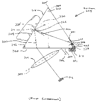
Figures 4 and 5 show a patterned object image acquisition system 308 in
accordance
with the present invention. Acquisition system 308 preferably includes a
triangular prism
310, a light source 312, a lens assembly 314, and an image sensor 316. Prism
310 is a five
faced triangular prism the length of which extends into the plane of Figure 4.
Prism 310
includes a rectangular, planar, imaging surface 318 against which an object to
be imaged,
such as a fingerprint 335, is placed. Prism 310 also includes a rectangular,
planar, viewing
surface 320 through which an image of a fingerprint 335 placed against imaging
surface
318 passes out of prism 310. In the embodiment of Figures 4 and 5, viewing
surface 320
also serves as a light receiving surface for allowing light to pass into prism
310. A light
scattering surface 322 comprises a third, or further, rectangular, planar,
surface of prism
310. For reasons detailed below, light scattering surface 322 is preferably a
diffusive.
Light source 312 is preferably an elongated LED array consisting of a single
row of
light emitting diodes (LEDs) extending the length (into the plane of Figure 4)
of prism 310.
If such LEDs are used as light source 312, a diffusive cover can be placed
between the
11
CA 02381300 2009-12-22
LEDs and viewing surface 320 to provide more even illumination of imaging
surface 318.
It is also within the ambit of the present invention, however, for light
source 312 to be any
other type of light source to provide incident light into prism 310.
Preferably, light source
312 is placed along an edge 338 of prism 310 which is opposite imaging surface
318.
However, it is also within the ambit of the present invention to configure and
locate a light
source for acquisition system 308 in any other way. For example, other
configurations for
light sources which can be used with the present invention are disclosed in
U.S. Patent No. 6,381,347 for "High, Contrast, Low Distortion Optical
Acquisition
System for Image Capturing" filed November 12, 1998. This includes placing
light
source 312 against viewing surface 320 anywhere between edge 338 and the line
360 along
viewing surface 320 formed by the intersection of viewing surface 320 and a
perpendicular
line to viewing surface 320 which intersects edge 365.
Lens assembly 314 is for receiving scattered light 330 from fingerprint 335
and
focusing scattered light 330 onto image sensor 316. Lens assembly 314 can be a
single
lens or, preferably, can consist of multiple lenses. Most preferably, lens
assembly 314 has
a focal length of approximately 13.48 mm and is located approximately 13.5 mm
from
viewing surface 320. Additionally, as shown in Figure 7 which is a schematic
diagram of
one embodiment of lens assembly 314, lens assembly most preferably consists of
three
lenses 904, 906, and 908 whose respective optical axes are aligned on a common
optical
axis 902. Lens 904 most preferably has a diameter of approximately 17.8 mm,
and both
lenses 906 and 908 most preferably have a diameter of approximately 6 mm. It
is
considered that any number of lenses be included in lens assembly 314.
Image sensor 3.16 captures optical light images from lens assembly 314
add=converts
them to electrical signals. Image -sensor 316 can be a charge couple device
("CCD") or any
other means of converting a light signal into either an analog or digital
electrical signal.
Preferably, image sensor 316 is a complementary metal oxide semiconductor
device. CCD
and CMOS image sensors are well known by those skilled in the art. The
electrical signals
generated by image sensor 316 can be processed using known means and used to
compare
input patterns, such as fingerprints. As noted in the Background section, such
signal
12
CA 02381300 2009-12-22
processing means are disclosed, for example, in U.S. Patent Nos. 4,135,147 and
4,688,995.
To create an optical image of fingerprint 335 on image sensor 316, fingerprint
335 is
placed against imaging surface 318. Incident light 324 from light source 312
passes
through viewing surface 320 and into prism 310. Because light source 312 is
located
adjacent to edge 338, incident light 324 strikes scattering surface 322. As
noted above,
scattering surface 322 is preferably diffusive. As such, a relatively high
portion of incident
light 334 striking scattering surface 322 is internally scattered in prism
310. This scattered
light then strikes imaging surface 318. Even if light scattering surface 322
is not diffusive,
substantially all of incident light 324 will strike scattering surface 322 at
an angle 323
which is greater than the critical angle for scattering surface 322. Thus,
incident light will
reflect off scattering surface 322 and strike imaging surface 318. To enhance
reflection of
incident light off scattering surface 322 it is contemplated to place a
mirrored face of a
reflecting surface 381 towards scattering surface 322.
Because incident light 324 has been scattered or directly reflected off
scattering surface
322, a relatively large percentage of incident light 324 will strike imaging
surface 318 at an
angle 327 less than the critical angle 328 of prism 310. Accordingly, incident
light 324
which strikes imaging surface 318 at a region thereof where there is a
fingerprint valley
309 will not undergo total internal reflection and will substantially pass
through imaging
surface 318. Thus, substantially no light hitting an area of imaging surface
318 where there
is a fingerprint valley 309 will be directed into the sensor 316. However,
incident light 324
that strikes a region of imaging surface 318 where there is a fingerprint
ridge 311 touching
imaging surface 318 will substantially scatter, producing scattered light 330.
A portion of
scattered light 330 will.exit prism.310 via viewing surface 320. Upon exiting
prism 310,
scattered light 330 will refract into lens assembly 314-which will focus
scattered light 330
into image sensor 316.
Because incident light 324 can be scattered by scattering surface 322,
incident light 324
provides relatively uniform illumination over imaging surface 318 which
produces a
relatively uniform image. Such a uniform image is desirable because it is
easier to process
and compare with other stored fingerprint data. To further increase the
uniformity of
13
CA 02381300 2002-02-04
WO 01/11549 PCT/US00/40530
illumination over imaging surface 318, the portion of viewing surface 320
facing light
source 312 can be streaked by etching lines 370, shown in Figure 5, on viewing
surface
320. Lines 370 run the length of prism 310 and parallel to apex 338. Lines 370
act to
diffuse light emitted from light source 312 as it passes through viewing
surface 320.
In addition to the components discussed above, image acquisition system 308
preferably also includes a light blocking shield 350 on a portion of light
receiving surface
adjacent to light source 312. Preferably, light blocking shield runs the
entire length of
prism 310 (into the plane of Figure 4). Light blocking shield 350 is to reduce
the amount
of stray light from light source 312 which might enter lens assembly 314 and
interfere with
or cloud a fingerprint image. It is also considered that the surface of light
blocking shield
350 facing the interior of prism 310 be mirrored. This mirroring can act to
desirably
increase the intensity of scattered light incident on imaging surface 318. In
addition to, or
instead of, light blocking surface 350, a second light blocking surface 352
can be placed
between light source 312 and lens assembly 314. Light shield 352 preferably
extends from
viewing surface 320 at an angle to block stray light from light source 312
from entering
lens assembly 314.
Because light source 312 is relatively narrow and located adjacent to edge 338
opposite
imaging surface 318, substantially all incident light 324 reaching imaging
surface 318 is
reflected or scattered into the lens assembly 314. That is, almost no incident
light 324 can
be captured by the image sensor 316 without scattering off the imaging surface
318 at the
points of contact with fingerprint ridges 311. To further reduce the
likelihood of incident
light 324 which falls into the fingerprint valleys 309 reaching image sensor
316 through
lens assembly 314, light source 312 is preferably configured not to extend
past a line 360,
shown in Figure 5, extending the length of prism 310 and defined by the
intersection of a
plane normal to viewing surface 320 and intersecting with edge 365, adjacent
to imaging
surface 318. If light source 312 is kept on the same side of this line as apex
338, then
substantially no incident light 324 emitted perpendicularly from light source
312 will reach
image sensor 316 without scattering off of the fingerprint ridges 311.
By minimizing the incident light 324 from light source 312 that is directly
incident on
imaging surface, there is substantially no total internal reflection of
incident light 324 from
regions of imaging surface 318 where there are fingerprint valleys 309. This
means that
14
CA 02381300 2002-02-04
WO 01/11549 PCTIUSOO/40530
substantially no light from these valley regions passes through viewing
surface 320 and
into lens assembly 314. Rather, substantially all the light passing into lens
assembly 314
from imaging surface 318 is scattered from fingerprint ridges 311 on imaging
surface 318.
This provides a fingerprint image having relatively high contrast between
fingerprint ridges
311 and valleys 309. Such a high contrast fingerprint image is relatively easy
to process
and compare with other fingerprint images and can, therefore, advantageously
increase
processing accuracy.
Further, use of this scattering technique for image acquisition is achieved
with a
triangular prism, as opposed to a trapezoidal prism as disclosed in Lougheed,
discussed in
the Background section. Because triangular prisms can be more efficient to
manufacture
than trapezoidal prisms, image acquisition system 308 can advantageously be
relatively less
expensive to manufacture.
Moreover, scattered light generally scatters from an object in many
directions, as
opposed to substantially one direction. And, as noted in the Background, non-
parallel
scattered light can be used by a lens assembly to form a focused image of an
object. Thus,
as shown in optical recognition system ", 18 in Figure 6, if the first lens of
lens assembly
314 has a smaller diameter than the diagonal of fingerprint 335 in viewing
surface 322,
non-parallel scattered light rays can be used to produce a focused image of
fingerprint 335.
Accordingly, lens assembly 314 can be, but does not necessarily need to be,
placed
relatively close to viewing surface 320 without loss of image quality near the
edges of a
fingerprint image generated by system 308. This advantageously allows the
image
acquisition system 308 to be relatively compact and allows lens assembly 314
to be
relatively low cost to manufacture.
Because, as shown in Figure 6, the diameter of a first lens of lens assembly
314 is
smaller than the size of the fingerprint on viewing surface 318, trapezoidal
distortion could
result in a generated image. However, the image acquisition system of the
current
invention can reduce trapezoidal distortion in, and increase the overall
sharpness of, a
produced image. As discussed in the Background section, trapezoidal distortion
is
manifested in an image having dimensions distorted from those of the actual
object being
imaged. Both trapezoidal distortion and portions of an image being out of
focus can be
CA 02381300 2002-02-04
WO 01/11549 PCT/US00/40530
caused by variation in path length of light from the apparent image of an
object to lens
assembly 314, and ultimately image sensor 316, from one part of the imaged
object to
another. As shown in Figure 6, however, in image acquisition system 308, the
path length
of scattered light 330 from different points on the apparent image 335' of
fingerprint 335 to
lens assembly 314 and image sensor 316 is substantially the same.
Specifically, path AA'
is substantially equal to path BB' and path CC'. Thus, trapezoidal distortion
can
advantageously be reduced and overall image sharpness can be increased. As
shown in
Figure 6, substantial equalization of paths AA', BB' and CC' is facilitated by
tilting lens
assembly 314 with respect to viewing surface 320.
However, unlike optical recognition system 108, shown in Figure 1, such
tilting of lens
assembly 314 does not severely reduce the intensity of the image reaching
image sensor
316. As noted in the background section with respect to optical recognition
system 108,
tilting lens assembly 114 causes reflected light 130 to strike the first
element of lens
assembly 314 at an angle to normal line thereof. This causes greater
reflection of reflected
light 130 from the surface of lens assembly 114, thereby undesirably reducing
image
intensity at image sensor 116.
However, prism 310 preferably has an index of refraction higher than 1. Thus,
scattered light 330 which strikes viewing surface 320 refracts away from the
normal to
viewing surface 320 as it exits prism 310. As such, by tilting the lens plane
307 of lens
assembly 314, scattered light 330 strikes lens assembly 314 at substantially
90 degrees.
Thus, there is little or no loss in image intensity due to undue reflection of
scattered light at
the surface of lens assembly 314, and trapezoidal distortion can be reduced,
and overall
image sharpness can be increased, without losing image intensity at image
sensor 316.
Referring to Figure 8, the appropriate angle at which to tilt lens assembly
314 can be
determined. In Figure 8, light rays 410 and 412 are scattered from imaging
surface edge
414 and opposite imaging surface edge 416, respectively. Lens plane 307 is a
theoretical
representation of lens assembly 314 as the thickness of the lens assembly goes
to zero.
Distance Aa is the distance from the apparent image of an object in prism 310
to lens plane
307 along light ray 410 and distance B'b is the distance from the apparent
image of an
object in prism 310 along light ray 412. In order to substantially eliminate
trapezoidal
16
CA 02381300 2002-02-04
WO 01/11549 PCT/US00/40530
distortion, distance Aa must be substantially equal to distance B'b. Because
B'b is the
apparent depth of an object at edge B in prism 310, then, as discussed in the
Background
section:
B'b=Bb/n
where Bb is the distance from point B, at edge 416, to point b on prism 310.
The
requirement for substantial elimination of trapezoidal distortion and
improvement in overall
image sharpness can be expressed as:
Aa = Bb/n (Eq. 1)
The angle of incidence of light ray 412 on viewing surface 320, that is, the
angle
between a normal line to viewing surface 320 and light ray 412 inside prism
310, is shown
in Figure 8 as 01. The angle of refraction of light ray 412 after it passes
out of prism 310 is
shown as 02. Thus, by Snell's law:
n = sin02/sin01 (Eq. 2)
Also, using fundamental trigonometric relationships, it can be shown that:
ABcos7 + Bbcosa' = Ab (Eq. 3)
where AB is the length of the imaging surface of prism 310 from point A to
point B; Ab is
the length of segment Ab on viewing surface 320; a' is the angle between light
ray 412 and
viewing surface 320, which equals 90 -01; and y is the angle between imaging
surface 318
and viewing surface 320 (also shown as angle 342 in Figure 8).
Finally, using the law of sines, it can be shown that:
AB/Bb = cos01/sing (Eq. 4)
17
CA 02381300 2002-02-04
WO 01/11549 PCTIUSOO/40530
Using equations 1, 2, 3, and 4 above, it can be shown that in order for
trapezoidal
distortion to be substantially eliminated, and overall image sharpness
increased, the
following condition relating the angles of prism 310 with the angle which lens
plane 307
forms with viewing surface 320 must be met:
(n2 - sin 28)2(coty)(sin6)+sin26 = 1 (Eq. 5)
Where, as shown in Figure 8, 6 is the angle that lens plane 307 of lens
assembly 314 forms
with viewing surface 320. Thus, imaging system 308, in accordance with the
present
invention, is preferably configured in accordance with equation 5 to
substantially eliminate
trapezoidal distortion and improve overall image sharpness.
However, in manufacturing imaging system 308, achieving precise tolerances for
angles y and 6 can be difficult and expensive. Therefore, an imaging system in
accordance
with the present invention and allowing for a 30% manufacturing tolerance is
preferably
configured in accordance with the equation 6 below:
0.7 (n2 - sin26)'2(coty)(sin6)+sin26 1.3 (Eq. 6)
More preferably, an imaging system in accordance with the present invention
and
allowing for a 15% manufacturing tolerance is configured in accordance with
equation 7
below:
0.85 -< (n2 - sin26)''/2(coty)(sin6)+sin26 1.15 (Eq. 7)
Most preferably, an imaging system in accordance with the present invention
and
allowing for a 7.5% manufacturing tolerance is configured in accordance with
equation 8
below:
0.925 (n2 - sin26)v(coty)(sin6)+sin26 1.075 (Eq. 8)
As noted above, by configuring imaging system 308 in accordance with one of
equations 5-8 above, trapezoidal distortion can be substantially reduced or
eliminated and
overall image sharpness can be improved. This advantageously facilitates more
accurate
image processing and comparison by an image acquisition system.
18
CA 02381300 2002-02-04
WO 01/11549 PCTIUSOO/40530
Prism 310 can be made of glass, acrylic or any other transparent material
having an
index of refraction higher than 1 (that of air). Prisms having the preferred
index of
refraction and angles are commercially available from Shinkwang Ltd. of Seoul,
Korea and
are fabricated of glass having the designation LaK-7 or LaK-8.
Lens assemblies such as lens assembly 314 are commercially available from
Woorim
Optical Systems Ltd. of Seoul, Korea and are preferably fabricated from a
glass having the
commercial designation of BK7. If more than one element is used in lens
assembly 314, as
shown in Figure 6, the individual elements can be aligned and spaced by
placing them in a
frame fabricated by plastic molding or any other fabrication means as is known
in the art.
Light source 312 preferably consists of four standard LEDs positioned in a
straight
array on a circuit board. Powering of LEDs is well known by those skilled in
the art.
Image sensor 316 is preferably a CMOS type sensor and is commercially
available from
Hyundai Electronics of Seoul, Korea, VLSI Vision, Ltd. of San Jose,
California, or
Omnivision Technologies Inc. of Sunnyvale, California.
To secure the components of image acquisition into the relative positions as
shown in
Figure 4, a frame having holding slots for each component can be plastic
molded or
otherwise fabricated. Light source 312 can be either placed in a holding slot
adjacent to
viewing surface 320 or attached directly to viewing surface 320 using adhesive
as known in
the art.
Equations 5-8 were derived assuming that the entire width AB of imaging
surface 318
would be used in capturing an image. However, less than the entire imaging
surface of a
prism can be used to capture an image. This may be the case, for example, if a
triangular
prism having an angle greater than or equal to 90 degrees is used as a light
refractor.
However, if the entire imaging surface of a prism is not used to image an
object, a
requirement in addition to being configured according to equations 5-8 above
is preferably
met by the configuration of such an imaging system. To illustrate this
additional
requirement, Figure 9 shows a triangular prism 510 having an obtuse angle 541.
Triangular
prism 510 includes a planar imaging surface 518, a planar viewing surface 520
and a planar
19
CA 02381300 2002-02-04
WO 01/11549 PCTIUSOO/40530
further surface 522. Figure 9 also shows a light source 512 which can be
substantially the
same as light source 312, and lens plane 507 of a lens assembly (not shown). A
lens
assembly used with prism 510 can be substantially the same as lens assembly
314.
As shown in Figure 9, a light ray 612 is scattered from point D on imaging
surface 518
and a light ray 610 is scattered from imaging surface 518 at point A. Prism
510 and lens
plane 507 are configured in accordance with equation 5 above. Additionally,
segment a'd'
is parallel to lens plane 507. And, length D'd' is the apparent depth in prism
510 of the
image of an object at point D on imaging surface 518. Thus, the length of
segments Aa'
and D'd' are the equal. Because the index of refraction of prism 510 is
greater than 1, as
light ray 612 leaves prism 510 at point d', it will refract away from a normal
line 620 to
viewing surface 520.
Angle 545, labeled as a' in Figure 9, which is the angle formed by the
intersection of
light ray 612 and viewing surface 520, and is adjacent to the intersection of
the viewing
surface and the imaging surface, is less than 90 degrees. Thus, as light ray
612 passes out
of prism 510 and refracts away from normal line 620, it will travel in a path
parallel to that
of light ray 610 outside of prism 510. Therefore, the lengths of segments a'a
and d'd are
also equal. Accordingly, the total path lengths from the apparent image in
prism 510 to the
lens plane 507, and ultimately the an image sensor (not shown) will be the
same for an
object on imaging surface 518 at both point A and point D. In this way overall
image
sharpness can be increased.
Referring now to Figure 10, which also shows prism 510, the path length from
the
apparent image in prism 510 of an object placed at point E on imaging surface
518 will not
be equal to the path length from the apparent image in prism 510 of an object
placed at
point A on prism 510. Light ray 612 is a scattered light ray from an object
placed at point
E on imaging surface 518. As above, because prism 510 has an index of
refraction which
is greater than 1, as light ray 612 exits prism 510 at point e', it will
refract away from
normal line 620 to viewing surface 520. Therefore, because angle 545, labeled
a', is
greater than 90 degrees, the path of light ray 612 outside of prism 510 is not
parallel to the
path of light ray 610 outside of prism 510. Because light rays 610 and 612 are
not parallel,
the length of segment e'e will be different from the length of segment a'a.
This means that
CA 02381300 2002-02-04
WO 01/11549 PCTIUSOO/40530
the total path length from the apparent image in prism 510 to lens plane 507
will be
different for an object at point E on imaging surface 318 than for an object
at point A
thereon. Thus, relatively large trapezoidal distortion and/or a relatively out
of focus image
will result.
As noted above, in order to avoid this, when a prism having a 90 degree or
greater
angle is used in an imaging system in accordance with the present invention,
preferably,
less than the entire width of the imaging surface is used to image an object.
As shown
above, when a' is less than 90 degrees, and the image capturing system is
configured
according to equations (5) through (8) above, trapezoidal distortion can be
substantially
eliminated. And, when a' is greater or equal to 90 degrees trapezoidal
distortion can result.
Thus, if less than the entire width of the imaging surface 518 of a prism is
to be used to
place an object to be imaged against, each portion of the imaging surface 518
to be used for
imaging must be able to have at least one light ray scattered therefrom such
that the
intersection of the one light ray and the viewing surface 520 form an angle,
a' in Figures 9
and 10, adjacent to the intersection of the viewing surface and the imaging
surface, which
is less than 90 degrees. This criteria advantageously facilitates reduction or
substantial
elimination of trapezoidal distortion and increase in overall image sharpness
in an imaging
system configured in accordance with one of equations 5-8 above.
Prism 510, and light source 512 can be manufactured in substantially the same
way and
of the same materials as discussed above with respect to prism 310 and light
source 312.
Many widely different embodiments of the present invention may be constructed
without departing from the spirit and scope of the present invention. It
should be
understood that the present invention is not limited to the specific
embodiments described
in the specification. For example, though the above disclosed embodiment of
the present
invention are described with reference to imaging a fingerprint, any other
type of patterned
object is contemplated to be imaged with the present invention.
21