Note: Descriptions are shown in the official language in which they were submitted.
CA 02381793 2002-02-11
WO 02/01765 PCT/USO1/20224
Outical Power and Wavelength Monitor
Field of the Invention
The invention relates to optical signal monitoring, and more particularly to
apparatus and methods for monitoring the wavelength and power of an optical
communication signal.
Backeround of the Invention
Modern optical fiber communication systems have high bandwidth and low
transmission loss. The bandwidth of an optical fiber determines how much
information can be transmitted without losing data due to degradation in the
optical
signal. Many modern optical fiber communication systems use Wavelength
Division
Multiplexing (WDM).
In WDM communication systems, separate signals having different carrier
wavelengths are transmitted simultaneously through a single optical fiber. The
number of wavelengths simultaneously propagating in a fiber is proportional to
the
bandwidth of the communication system. Each wavelength bandwidth occupies a
certain channel spacing in the communication system. The more closely spaced
the
Garner wavelengths, the more channels that can be propagated simultaneously.
However, as the spacing between the wavelengths becomes smaller, the
probability of
cross talk between channels increases. This cross talk is undesirable because
data
from one channel interferes with data fiom another channel, thereby causing
erroneous data to be propagated in the communication system and ultimately
corrupting the data at the receiver.
In order to maximize the number of available channels in a WDM
communication system, each laser source must generate an optical beam having a
relatively stable wavelength. The lasers used for WDM transmitters generally
emit
light at a stable wavelength and the wavelength can be precisely controlled.
However, many laser sources experience wavelength drift over time caused by
temperature, aging, and modal instability. Wavelength drift can cause cross
talk and
CA 02381793 2002-02-11
WO 02/01765 PCT/USO1/20224
result in a loss of data in WDM communication systems and, therefore, must be
monitored and compensated.
Numerous apparatus and methods have been used to monitor the wavelength
of optical signals in WDM communication systems. Some of these apparatus and
methods split an input signal into two signals and filter one signal with a
low-pass
filter and the other signal with a high-pass filter. The altered signals are
directed to
two closely spaced detectors. The electrical signals generated by the two
detectors are
then compared. By selecting the characteristics of the filters correctly, the
wavelength
of the optical signals can be precisely determined and monitored.
Other apparatus and methods used to monitor the wavelength of optical
signals in WDM communication systems use a channel selector, such as a crystal
grating or diffraction grating, and a wavemeter to monitor the optical
signals. For
example, in one prior art apparatus, an optical signal is first separated into
channels by
a channel selector and then propagated to a wavemeter that monitors the
wavelength
of the optical signal in each channel.
These prior art wavelength monitors are generally impractical for modern high
capacity optical communication systems because they are complex and occupy
relatively large volumes. In addition, these prior art wavelength monitors use
differential detection methods to measure the wavelength of the communication
signal, which can result in erroneous measurements. These differential
detection
methods require at least two photodetectors that each sample different
portions of the
waveguide mode.
Measuring different portions of the waveguide mode can lead to uncertainty in
the measured wavelength due to modal instability. These uncertainties can
result in
erroneous measurements, which can result in incorrect compensation. If the
waveguide is a single mode optical fiber, the mode is typically very stable.
However,
if the waveguide is multimode, there are modal instabilities under some
conditions.
There are several factors, which cause modal stability in the propagation
media.
These factors include the level of injection current, the condition of the
facet coating,
the efficiency and the operating temperature.
CA 02381793 2002-02-11
WO 02/01765 PCT/USO1/20224
Summar~of the Invention
The present invention relates to wavelength and power monitors, which do not
experience the disadvantages of differential detection and other prior art
methods of
monitoring wavelength. A principle discovery of the present invention is that
an
optical wavelength and power monitor can be constructed to monitor one portion
of
the mode of a single optical beam and can substantially simultaneously
determine the
wavelength and the optical power of a single optical beam.
Accordingly, the present invention features an optical beam monitor that
includes a first detector positioned in the path of an optical beam. In one
embodiment, the first detector comprises a semitransparent photodiode that
transmits
a portion of the optical beam. The first detector may include an anti-
reflection
coating that prevents a portion of the optical beam from reflecting off of the
first
detector. The first detector generates an electrical signal that is
proportional to the
optical power of the incident optical beam.
An optical filter, such as a Fabry-Perot filter or a thin film filter, is
positioned
in the path of the optical beam and passes a portion of the optical beam
corresponding
to a wavelength within the bandwidth of the optical filter. In one embodiment,
the
optical filter comprises a narrow band-pass filter. A substrate may be
disposed
between the first detector and the optical alter. In one embodiment, the
substrate is
formed of glass. In one embodiment, the substrate includes an anti-reflection
coating
a
on at least one end of the substrate to prevent reflections. In another
embodiment, a
glass wedge is disposed between the first detector and the optical filter in
order to
deflect any reflected beams away from the first photodiode, thereby reducing
the
detection of erroneous signals. The glass wedge may include an anti-reflection
coating to prevent reflections.
A second detector is positioned in the path of the optical beam. The second
detector generates a second electrical signal that is proportional to the
optical power
of the filtered optical beam. A processor is electrically coupled to the first
and second
detector and is used to generate a signal that characterizes the wavelength
and power
of the optical beam. This signal can be used to control the wavelength and
power of
the optical source that generates the optical beam.
-3-
CA 02381793 2002-02-11
WO 02/01765 PCT/USO1/20224
The present invention also features an apparatus for monitoring the optical
power and the wavelength of optical signals in a wavelength division
multiplexed
communication system. The apparatus includes a mufti-wavelength laser that
generates an optical beam. A~ first detector is positioned in a path of the
optical beam.
The first detector generates a first electrical signal that is proportional to
an optical
power of the optical beam transmitting in the communication system. An optical
filter is positioned in the path of the optical beam. The optical filter
transmits a
portion of the optical beam that corresponds to a channel of the communication
system.
A second detector is positioned in the path of the optical beam. The second
detector generates a second electrical signal that is proportional to an
optical power of
the filtered optical beam corresponding to the channel. A signal processor
receives
the first and second electrical signals. The signal processor generates at
least one
signal that corresponds to the wavelength and power of the optical beam
transmitting
in the communication system. This signal can be used to control the wavelength
and
power of the mufti-wavelength laser.
The present invention also features a method for monitoring the wavelength
and power of an optical beam. The method includes detecting an optical beam
and
generating a first electrical signal that corresponds to an optical power of
the optical
beam. A portion of the optical beam having a wavelength within a predetermined
bandwidth is then detected. A second electrical signal is generated that
corresponds
to an optical power of the portion of the optical beam within the
predetermined
bandwidth. The first and second electrical signals are processed and a signal
is
generated that characterizes the optical beam. In one embodiment, the signal
controls
a source that generates the optical beam.
The above and other objects, features and advantages of the present invention
and the manner of realizing them will become more apparent, and the invention
itself
will best be understood from a study of the following description and appended
claims with reference to the attached drawings showing some of the numerous
embodiments of the invention.
-4-
CA 02381793 2002-02-11
WO 02/01765 PCT/USO1/20224
Brief Description of the Drawings
Fig. 1 is a schematic diagram of a prior art wavelength monitor that uses
differential detection.
Fig. 2 is a graph that illustrates the output characteristics of the first and
second detector of the prior art wavelength monitor of Fig. 1.
Fig. 3 is a schematic diagram of one embodiment of a wavelength and power
monitor of the present invention.
Fig. 4 is a schematic diagram of another embodiment of the wavelength and
power monitor of the present invention that does not include a substrate.
Fig. 5 is a schematic diagram of another embodiment of the wavelength and
power monitor of the present invention that includes a Fabry-Perot filter.
Fig. 6 is a schematic diagram of one embodiment of the wavelength and power
monitor of the present invention that includes a beam splitter.
Fig. 7 is a schematic diagram of another embodiment of the wavelength and
power monitor of the present invention that includes a glass wedge.
Fig. 8 is a schematic diagram of another embodiment of the wavelength and
power monitor of the present invention that includes a glass substrate with a
Fabry-
Pexot filter and a beam splitter.
Fig. 9 is a schematic diagxam of a broadband wavelength and power monitor
of the present invention that includes a wideband thin film filter for course
wavelength monitoring and a Fabry-Perot Etalon for fine wavelength monitoring.
Fig. 10 is a schematic diagram of an optical communication system that
includes the wavelength and power monitor of the present invention to control
the
output of a tunable laser.
Detailed Description
Fig. 1 is a schematic diagram of a prior art wavelength monitor 10 that uses
differential detection. A source 12 generates an optical beam 14. A beam
sputter 16
-5-
CA 02381793 2002-02-11
WO 02/01765 PCT/USO1/20224
samples a portion of beam 14 and directs a sampled beam 18 to a second beam
splitter
20. The second beam splitter 20 splits the sampled beam into a first 22 and
second
sampled beam 24. The second beam splitter 20 directs the first sampled beam 22
to a
low pass filter 26 and the second sampled beam 24 to a high pass filter 28.
The
monitor 10 uses a mirror 30 to direct the second sampled beam 24 to the high
pass
filter 28. A first detector 32 measuxes the optical power of the beam
transmitting
though the Iow pass filter 26. A second detector 34 measures the optical power
of the
beam transmitting through the high pass filter 28.
Fig. 2 is a graph that illustrates the output characteristics of the first 32
and
second detector 34 of the prior art wavelength monitor of Fig. 1. The first
detector 32
measures a low pass characteristic 36. The second detector 34 measures a high
pass
characteristic 38. The center frequency of both the low pass 32 and high pass
filter 34
is generally chosen to approximate the wavelength of the optical beam 14
generated
by source 12.
In operation, as the wavelength of the optical beam 14 changes, the optical
power detected by the first 32 detector changes in a direction that is
inversely
proportional to the change in the optical power detected by the second
detector 34.
Therefore, the wavelength of the optical beam 14 can be monitored by measuring
the
ratio of optical power detected by the first 32 detector to the optical power
detected by
the second detector 34. This ratio is a sensitive measure of the change in the
wavelength of the optical beam generated by source 12. This method, however,
uses
two photodetectors that measure different portions of the optical mode.
Therefore,
this method is subject to uncertainty in the measured wavelength due to modal
instability as described above.
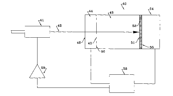
Fig. 3 is a schematic diagram of one embodiment of a wavelength and power
monitor 40 of the present invention. The monitor 40 includes an optical source
41
that generates an incident optical beam 42. A collimating lens (not shown) may
be
positioned in the path of the incident optical beam 42. In one embodiment, the
optical
source 41 is a tunable semiconductor laser that is suitable for use in a
wavelength
division multiplexed (WDM) communication system. For example, the optical
source
41 may be a distributed feedback semiconductor laser.
-6-
CA 02381793 2002-02-11
WO 02/01765 PCT/USO1/20224
The monitor 40 also includes a first photodiode 44 that is partially
transparent.
The first photodiode 44 generates a first electrical signal that is
proportional to the
optical power of the incident optical beam 42. A portion of the optical beam
42 is
transmitted through an exit surface 43 of the first photodiode 44. The first
photodiode
44 may include an anti-reflection (AR) coating on an incident surface 46 to
reduce
reflections from the incident surface.
The first photodiode 44 is mounted to a substrate 48 that is at least
partially
transparent. The substrate 48 may comprise glass. The substrate 48 may have an
AR
coating on an incident surface 50 to prevent reflected light from striking the
first
photodiode 44 and generating an erroneous signal. In another embodiment, the
substrate 48 is wedge shaped in order to deflect any reflected beams away from
the
first photodiode 44, thereby preventing erroneous signals.
The monitor 40 also includes a thin film optical filter 52 that is positioned
on
an exit surface 51 of the substrate 48. In another embodiment; free
space'separates
the first photodiode 44 from the thin elm optical filter 52 and the filter 52
is
positioned in the direction of propagation of the optical beam 42. The thin
film filter
52 may be a narrow band-pass filter.
A second photodiode 54 is positioned adjacent to the thin film filter 52 in
the
direction of propagation of beam 42. The second photodiode 54 generates an
electrical signal that is proportional to the optical power of the filtered
portion of the
optical beam 42. The second photodiode 54 may include an AR coating on an
incident surface 56 to reduce reflections that can be detected by the first
photodiode
44 and that can result in erroneous signals.
A signal processor 58 receives the first and second electrical signals and
generates an output signal that characterizes the optical beam. In one
embodiment,
the signal processor 58 generates a signal that is proportional to the ratio
of the optical
power of the filtered portion of the optical beam P~, to the optical power of
the incident
optical beam Pmon. That is, the signal processor generates a signal that is
proportional
to P~,/P",on. In another embodiment, the signal processor generates a signal
that is
proportional to the ratio of the difference between P~, and Pmo" to the sum of
P~, and
Pmon. That is, the signal processor generates a signal that is proportional to
(P~, -
CA 02381793 2002-02-11
WO 02/01765 PCT/USO1/20224
Pmon)l(Pa, + Pmon). Thus in one embodiment of the invention, the wavelength
transfer
function of the monitor 40 can be either P~,/P",on or (P~, - Pmon)~(Pa. +
Pmon).
The output signal of the signal processor 58 can be used to control the
wavelength and power of the optical source 41. In one embodiment, the optical
source 41 is a tunable laser and an output of the signal processor 58 is
electrically
connected to a source controller 59. The signal generated by the signal
processor
causes the source controller 59 to change the wavelength and power of the
optical
source 41.
In operation, the first photodiode 44 generates an electrical signal that is
proportional to the optical power of the incident optical beam 42 (Pmon)~ The
portion
of the incident optical beam that was not absorbed by the first photodiode 44
propagates through substrate 48 to filter 52. Filter 52 transmits a portion of
the
optical beam 42 that has a wavelength within a predetermined bandwidth. The
filtered portion of the optical beam 42 is then detected by the second
photodiode 54.
The second photodiode 54 generates an electrical signal that is proportional
to the
optical power of the filtered portion of the optical beam (P~,).
The signal processor 58 generates a signal that characterizes the optical
beam.
The signal may be proportional to P~,/P",on or may be proportional to (P~, -
P",o")/(P~, +
Pmon). From the signal generated by the signal processor 58, changes in the ,
wavelength and the optical power of the incident beam 42 can be monitored.
In one embodiment, the monitor 40 includes a source controller 59 that is
electrically connected to an output of the signal processor 58. The source
controller
59 receives the signal from the signal processor 58 and adjusts the wavelength
and
power of the optical source 41. In one embodiment, the source controller 59 is
a
thermo-electric cooler and the source controller 59 adjusts the temperature of
the
optical source 41. In another embodiment, the source controller 59 is a laser
drive
current controller 59 and the source controller 59 adjusts the drive current
of the
optical source 41.
Fig. 4 is a schematic diagram of another embodiment of the wavelength and
power monitor 60 of the present invention. The monitor 60 is similar to the
monitor
_g_
CA 02381793 2002-02-11
WO 02/01765 PCT/USO1/20224
40 described in connection with Fig. 3. The monitor 60 includes a first
photodiode 44
that is partially transparent. The first photodiode 44 generates a first
electrical signal
that is proportional to the optical power of the incident optical beam 42. The
first
photodiode 44 may include an AR coating on an incident surface 46 to reduce
reflections from the incident surface.
The monitor 60 does not have a substrate. Instead, the monitor 60 includes a
thin film optical filter 52 that is positioned directly adjacent to the first
photodiode 44
in the direction of propagation of optical beam 42. The thin film filter 52
may be a
narrow band-pass filter. A second photodiode 54 is positioned adjacent to the
thin
film filter 52 in the direction of propagation of optical beam 42. The second
photodiode 54 generates an electrical signal that is proportional to the
optical power
of the filtered portion of the optical beam 42. The second photodiode 54 may
include
an AR coating on an incident surface 56 to reduce reflections that can be
detected by
the first photodiode 44.
A signal processor 58 receives the first and second electrical signals and
generates an output signal that characterizes the optical beam. In one
embodiment of
the invention, the signal processor 58 generates a signal that is proportional
to P~,/Pmon
or (P~, - P,T,on)/(Pa, + Pmo"). From the signal generated by the signal
processor 58,
changes in the wavelength and the optical power of the incident beam 42 can be
monitored. In one embodiment, the monitor 60 includes a source controller 59
that is
electrically coupled to the output of the signal processor 58. The source
controller 59
controls the wavelength and power of the optical source 41 as described in
connection
with Fig. 3. The operation of the monitor 60 is similar to the operation of
monitor 40
described in connection with Fig. 3.
Fig. 5 is a schematic diagram of another embodiment of the wavelength and
power monitor 70 of the present invention that includes a bulk Fabry-Perot
(FP) filter.
The monitor 70 is similar to the monitor 40 described in connection with Fig.
3. The
monitor 70 includes a first photodiode 44 that is partially transparent. The
first
photodiode 44 generates a first electrical signal that is proportional to the
optical
power of the incident optical beam 42. The first photodiode 44 may include an
AR
coating on an incident surface 46 to reduce reflections from the incident
surface.
_g_
CA 02381793 2002-02-11
WO 02/01765 PCT/USO1/20224
The monitor 70 includes a bulk Fabry-Perot filter 49 that is positioned
adjacent to the first photodiode 44 in the direction of propagation of beam
42. The
Fabry-Perot filter 49 has a first partially reflecting mirror 71 positioned at
one end
adjacent to the first photodiode 44 and a second partially reflecting mirror
72
positioned at a second end. The Fabry-Perot filter 49 produces a repetitive,
comb-like
transmittance and reflectance.
A second photodiode 54 is positioned adjacent to the Fabry-Perot filter 49 in
the direction of propagation of beam 42. The second photodiode 54 generates an
electrical signal that is proportional to the optical power of the filtered
portion of the
optical beam 42. The second photodiode 54 may include an AR coating on an
incident surface 56 to reduce reflections that can be detected by the first
photodiode
44.
A signal processor 58 receives the first and second electrical signals and
generates an output signal that characterizes the optical beam. The signal
processor
58 rnay generate a signal that is proportional to P~/Pmon or a signal that is
proportional
(P~, - P"~oa)~(P~, + Pmon). In one embodiment, the monitor 70 includes a
source
controller 59 that is electrically coupled to the output of the signal
processor 58. The
source controller 59 controls the wavelength and power of the optical source
41 as
described in connection with Fig. 3.
Fig. 6 is a schematic diagram of another embodiment of the wavelength and
power monitor 75 of the present invention that includes a beam sputter 90. In
one
embodiment, the beam sputter 90 comprises a non-polarizing beam splitter. The
beam
splitter 90 includes a partially reflecting mirror deposited on a hypotenuse
98 that
transmits a portion of the beam in the direction of propagation of the
incident beam 42
and reflects a portion of beam in the direction perpendicular to the direction
of
propagation of incident beam 42. Beam splitter 90 may have an AR coating
deposited
on at least one of an incident surface 92 and an exit surface 94.
The monitor 75 includes a first photodiode 44 that is positioned in the
direction perpendicular to the direction of propagation of incident beam 42.
The first
photodiode 44 generates a first electrical signal that is proportional to the
optical
-10-
CA 02381793 2002-02-11
WO 02/01765 PCT/USO1/20224
power of the incident optical beam 42. The first photodiode 44 may include an
AR
coating on an incident surface to reduce reflections from the incident
surface.
A thin film filter 52 is positioned in the direction of propagation of beam
42.
A second photodiode 54 is positioned adjacent to the thin film filter 52 in
the
direction of propagation of beam 42. The second photodiode 54 generates an
electrical signal that is proportional to the optical power of the filtered
portion of the
optical beam 42. The second-photodiode 54 may include an AR coating to reduce
reflections that can be detected by the first photodiode 44. The thin film
filter 52 may
be deposited onto beam splitter 90 or onto photodiode 54 or may be positioned
between the beam splitter 90 and the photodiode 54.
A signal processor 58 receives the first and second electrical signals and
generates an output signal that characterizes the optical beam. The operation
of the
monitor 75 is similar to the operation of the other embodiments of the monitor
of the
present invention. The signal processor 58 may generate a signal that is
proportional
to P~,/PI"on or a signal that is proportional (P~, - Pr"on)/(P~, + Pmon). In
one embodiment,
the monitor 75 includes a source controller 59 that is electrically coupled to
the output
of the signal processor 58. The source controller 59 controls the wavelength
and
power of the optical source 41 as described in connection with Fig. 3.
The monitor of the present invention has numerous other embodiments that
use a beam splitter. For example, in one embodiment of the monitor (not
shown), a
first photodiode is positioned after the beam splitter in the direction of
propagation of
incident beam. A thin film filter and second photodiode are positioned after
the beam
splitter in the direction perpendicular to the incident beam. The operation of
this
embodiment is similar to the operation of the monitor of Fig 6 and the
wavelength
transfer function of this embodiment can also be represented by (P~,/PI"o") or
by (P~, -
Pmon)/(Pa, + Pmo"), where Pmon is proportional to the output electrical signal
of
photodiode and P~, is proportional to the output of the second photodiode.
Fig. 7 is a schematic diagram of another embodiment of the wavelength and
power monitor 100 of the present invention that includes a glass wedge 102.
The
glass wedge 102 is similar to the beam splitter 90 of Fig. 6. The glass wedge
102
transmits a portion of the beam in the direction of propagation of the
incident beam 42
-11-
CA 02381793 2002-02-11
WO 02/01765 PCT/USO1/20224
and reflects a portion of beam in a direction perpendicular to the direction
of
propagation of incident beam 42.
The monitor 100 includes a first photodiode 44 that is positioned
perpendicular to the direction of propagation of incident beam 42. The first
photodiode 44 generates a first electrical signal that is proportional to the
optical
power of the incident optical beam 42. The first photodiode 44 may include an
AR
coating on an incident surface to reduce reflections from the incident
surface.
A thin film filter 52 is deposited or positioned on the hypotenuse 98 of the
glass wedge. A second photodiode 54 is positioned adj scent to the thin film
filter 52
in the direction of propagation of beam 42. The second photodiode 54 generates
an
electrical signal that is proportional to the optical power of the filtered
portion of the
optical beam 42. The second photodiode 54 may include an AR coating to reduce
reflections that can be detected by the first photodiode 44.
A signal processor 58 receives the first and second electrical signals and
generates an output signal that characterizes the optical beam. The operation
of the
monitor 75 is similar to the operation of the other embodiments of the monitor
of the
present invention. The signal processor 58 may generate a signal that is
proportional
to P~,/P",on or a signal that is proportional (P~, - P",on)/(P~, + Pmon). In
one embodiment,
the monitor 60 includes a source controller 59 that is electrically coupled to
the output
of the signal processor 58. The source controller 59 controls the wavelength
and
power of the optical source 41 as described in connection with Fig. 3.
Fig. 8 is a schematic diagram of another embodiment of the wavelength and
power monitor 150 of the present invention that includes a glass substrate
with a
Fabry-Perot filter 49 and a beam sputter 90. The beam splitter 90 has a
partially
reflecting mirror deposited on a hypotenuse 98 that transmits a portion of the
beam in
the direction of propagation of the incident beam 42 and reflects a portion of
beam in
a direction perpendicular to the direction of propagation of incident beam 42.
Beam
splitter 90 may have an AR coating deposited on at least one of an incident
surface 92
and an exit surface 94.
A bulk Fabry-Perot filter 49 is positioned in the direction of propagation of
the
incident beam 42. The Fabry-Perot filter 49 has a first partially reflecting
mirror 71
-12-
CA 02381793 2002-02-11
WO 02/01765 PCT/USO1/20224
positioned at an incident end and a second partially reflecting mirror 72
positioned at
an exit. The Fabry-Perot filter 49 produces a repetitive, comb-like
transmittance and
reflectance.
The monitor 150 includes a first photodiode 44 that is positioned
perpendicular to the direction of propagation of incident beam 42. The first
photodiode 44 generates a first electrical signal that is proportional to the
optical
power of the incident optical beam 42. The first photodiode 44 may include an
AR
coating on an incident surface to reduce reflections from the incident
surface. The
optical power detected by the first photodiode 44 is independent of the beam
reflected
from the Fabry-Perot filter 49.
The monitor 150 includes a second photodiode 54 that is positioned adjacent
to the Fabry-Perot filter 49 in the direction of propagation of the incident
beam. The
second photodiode 54 generates an electrical signal that is proportional to
the optical
power of the filtered portion of the incident beam 42.
A signal processor 58 receives the first and second electrical signals and
generates an output signal that characterizes the optical beam 42. The
operation of
the monitor 150 is similar to the operation of the other embodiments of the
monitor of
the present invention. The signal processor 58 may generate a signal that is
proportional to Pa/Pmo" or a signal that is proportional (P~, - P",on)~(P~, +
Pmo"). In one
embodiment, the monitor 150 includes a source controller 59 that is
electrically
coupled to the output of the signal processor 58. The source controller 59
controls the
wavelength and power of the optical source 41 as described in connection with
Fig. 3.
Fig. 9 is a schematic diagram of a broadband wavelength and power monitor
200 of the present invention that includes a wideband thin film filter for
course
wavelength monitoring and a Fabry-Perot Etalon for fine wavelength monitoring.
The monitor 200 includes an optical source 41, such as a tunable semiconductor
laser,
that generates an optical beam 42. A collimating lens (not shown) may be
positioned
in the path of the incident optical beam 42.
A beam splitter 90 is positioned in a path of the optical beam 42. In one
embodiment, the beam splitter 90 comprises a non-polarizing beam splitter. The
beam splitter 90 includes a partially reflecting mirror deposited on a
hypotenuse 98
-13-
CA 02381793 2002-02-11
WO 02/01765 PCT/USO1/20224
that transmits a portion of the beam in the direction of propagation of the
incident
beam 42 and reflects a portion of beam in the direction perpendicular to the
direction
of propagation of incident beam 42. Beam splitter 90 may have an AR coating
deposited on at least one of an incident surface 92 and an exit surface 94.
The monitor 200 includes a second beam splitter 202 that is positioned in the
path of the portion of beam in the direction perpendicular to the direction of
propagation of incident beam 42. The second beam splitter 202 splits the
reflected
portion of the beam into a first 204 and a second optical path 206. In one
embodiment, the second beam splitter 202 is a cylindrical lens.
A ftrst photodiode 208 is positioned in the first path 204. The first
photodiode
208 generates a ftrst electrical signal that is proportional to the optical
power of the
incident optical beam 42. The first photodiode 208 may include an AR coating
on an
incident surface 209 to reduce reflections from the incident surface 209.
A coarse ftlter 210 is positioned in the second path 206. In one embodiment,
the coarse filter 210 comprises a thin film filter. The coarse filter 210
passes a
relatively broadband optical signal. A second photodiode 212 is positioned
after the
coarse filter 210 in the second path 206. The second photodiode 212 generates
a
second electrical signal that is proportional to the optical power of the
broadband
optical signal.
A Fabry-Perot Etalon 214 is positioned in the direction of propagation of the
incident beam 42. A Fabry-Perot Etalon or Fabry-Perot interferometer is a
relatively
ftne wavelength or narrow band filter that passes optical signals having
multiple
wavelengths corresponding to the multiple optical paths of the Fabry-Perot
Etalon
214. A third photodiode 216 is positioned in the direction of propagation of
the
incident beam 42 after the Fabry-Perot Etalon 214. The third photodiode 216
detects
the multiple wavelengths corresponding to the multiple optical paths of the
Fabry-
Perot Etalon 214 and generates a third electrical signal that is proportional
to the
optical power in the beam transmitted by the Fabry-Perot Etalon 214.
A signal processor 58 receives the ftrst, second, and third electrical signals
and
generates an output signal that characterizes the optical beam 42. The signal
processor 58 may generate a signal that is proportional to P~,/P",on or a
signal that is
-14-
CA 02381793 2002-02-11
WO 02/01765 PCT/USO1/20224
proportional (I'~, - Pmon)~(Pa, + Pmon). In one embodiment, the monitor 200
includes a
source controller 59 that is electrically coupled to the output of the signal
processor
58. The source controller 59 controls the wavelength and power of the optical
source
41 as described in connection with Fig. 3.
Fig. 10 is a schematic diagram of an optical communication system 250 that
includes the wavelength and power monitor of the present invention 252 to
control the
output of a tunable laser 254. The tunable laser 254 is optically coupled to
an optical
modulator 256. The optical modulator 256 modulates the output of the tunable
laser
254 and generates a modulated optical beam. In one embodiment, the modulated
optical beam is coupled into an optical fiber of the optical communication
system. A
portion of the modulated optical beam is coupled into the wavelength and power
monitor 252. In one embodiment, the modulator is a Mach Zehnder interferometer
and the wavelength and power monitor 252 is optically coupled to the second
port of
the interferometer.
The wavelength and power monitor 252 can be any monitor according to the
present invention. For example, the monitor 252 can be the broadband monitor
described in connection with Fig. 9. In this embodiment, the monitor 252
generates a
first, second and third electrical signal. A signal processor 258 receives the
first,
second, and third electrical signals and generates a signal at an output that
characterizes the optical beam 42.
The output of the signal processor 258 is electrically coupled to an input of
a
tunable laser controller 260. The tunable laser controller 260 receives the
signal
generated by the signal processor and controls the optical power and
wavelength of
the laser. In one embodiment, the tunable laser controller 260 is a
thermoelectric
cooler and that controls the tunable laser 254 by controlling the temperature
of the
laser. In another embodiment, the tunable laser controller 260 is a laser
drive current
controller and controls the tunable laser 254 by changing the drive current of
the laser.
The wavelength and power monitor of the present invention has numerous
advantages over prior art monitors. One advantage is that the monitor of the
present
invention monitors one portion of the mode of a single optical beam and
substantially
simultaneously determines the wavelength and the optical power of a single
optical
-15-
CA 02381793 2002-02-11
WO 02/01765 PCT/USO1/20224
beam. Monitoring one portion of the mode of a single optical beam avoids the
problems associated with differential detection that are described above.
Since the
monitor of the present invention samples the same potion of the beam, it is
less
susceptible to the modal stability of the optical source being monitored. This
feature
improves the long-term stability of the monitor. This feature also enables
semiconductor laser sources to be operated in a constant power mode instead of
a
constant current mode. This is because the mode structure of semiconductor
lasers is
dependent on the injection current of the laser.
-16-
CA 02381793 2002-02-11
WO 02/01765 PCT/USO1/20224
Equivalents
While the invention has been particularly shown and described with reference
to specific preferred embodiments, it should be understood by those skilled in
the art
that various changes in form and detail may be made therein without departing
from
the spirit and scope of the invention as defined by the appended claims.
-17-