Note: Descriptions are shown in the official language in which they were submitted.
CA 02381803 2002-02-11
WO 01/20347 PCT/DK00/00513
1
NANO-DRIVE FOR HIGH RESOLUTION POSITIONING AND FOR POSITIONING
OF A MULTI-POINT PROBE
Field of the invention
The present invention generally relates to a nano-drive for high resolution
positioning
and for positioning of a multi-point probe and further relates to the
technique of testing
electric properties on a specific location of a test sample and in particular
the tech-
nique of probing and analysing semiconductor integrated circuits for example
of LSI
and VLSI complexity.
Description of the related art
A method for creating very small movements by means of inertial force is known
from
the literature, for example US pat. 5229679. This method will now be described
re-
ferring to fig. 17.
An apparatus for creating very small movements according to prior art,
comprises a
support 1701, a movable part 1703, a piezoelectric element 1705 and an
inertial part
1707. The movable part 1703 is held against the support 1701 by means of
gravita-
tion or a spring-load. The piezoelectric element can be contracted or
elongated by
applying an electrical field to the element. If the contraction or elongation
occur slowly,
the frictional force between the support and the movable part will prevent any
movement of the movable part. However, when the electrical field on the
movable part changes in such a way that the piezoelectric element contract or
elongates quickly, the force on the movable part can exceed the frictional
force be-
tween the movable part and the substrate, causing the movable part to change
its position relative to the substrate with a fraction of a micrometer. In
this
way a slow contraction followed by a quick elongation will cause the movable
part to
change position. This is shown in figure 17a-c. By repeated slow contraction
and
quick elongation of the element, the movable part can travel over several
milli-
meters. The movable part can be made to travel in the opposite direction by
repeated quick contraction and slow elongation of the piezoelectric element as
shown in figure 17d-f.
CA 02381803 2002-02-11
WO 01/20347 PCT/DK00/00513
2
In the prior art, only the change in length of the piezoelectric element in
the
direction of movement is used to create the movement of the movable part. The
time
dependence of the electrical field on the piezoelectric element for providing
the
movement is described in the literature as a sawtooth curve-form (for example
US
Pat. 5568004).
In the prior art, all realizations of the known motion principle use the
moving part 1703
to move a body fixed to said part relative to another body which is fixed to
the under-
lying support 1701. Furthermore, in all existing realizations of the known
motion prin-
ciple the frictional forces are induced by outer forces such as gravitational
forces,
electro-mechanical forces, or external spring-loads in a highly asymmetrical
manner.
The most commonly used technique of testing the electric properties of a test
sample
involves the generation of resistivity or carrier concentration profiles of
the surface of a
processed semiconductor wafer by the utilisation of a four-point probe as
described in
published international patent application WO 94/11745. Furthermore, see for
example
S.M. Sze, Semiconductor devices - Physics and Technology, Wiley New York
(1985).
As shown generally in figure 1, the conventional four-point probe technique
typically
has the points positioned in an in-line configuration. By applying a current
to the two
peripheral points as shown in detail in figure 2, a voltage can be measured
between
the two inner points of the four point probe. Thus the electric resistivity of
the test
sample can be determined through the equation
p = c ~ (VII ),
wherein V is voltage measured between inner points, wherein I is current
applied to
the peripheral points and, wherein c is a geometry factor depending on the
surface
contact separation d and the dimensions of the test sample. Several schemes
for
calculating the correction factors have been developed, see F.M. Smits,
Measurement
of Sheet Resistivities with the Four-Point Probe, Bell System Technical J. 37,
711
(1958), EP 0 299 875 B1, and J. Shi and Y. Sun, New method for calculation of
the
correction factors for the measurement of sheet resistivity of a square sample
with a
square four-point probe, Rev. Sci. Instrum. 68 1814 (1997).
CA 02381803 2002-02-11
WO 01/20347 PCT/DK00/00513
3
The four-point probe generally consists of four tungsten or solid tungsten
carbide tips
positioned into contact with a test sample, being for example a semiconductor
wafer.
An external positioning system places the four-point probe into physical
contact with
the semiconductor wafer by moving the four-point probe in a perpendicular
motion
relative to the wafer surface. Pressure perpendicular to the wafer surface has
to be
applied to the four-point probe, in order to ensure that all four points
obtain physical
contact with for example an uneven wafer surface. Hence the pressure from the
tips
on the surface varies between the tips. The tips are separated by a distance
d, shown
in figure 1, typically in the order of 0.5 mm.
An alternative to the above described four-point probe is the SR (Spreading
Resis-
tance) probe, described in US Patent No. 5,347,226 and hereby incorporated in
this
description by reference. The SR probe consists of two probe tips situated on
one
cantilever arm. The SR probe is brought into physical contact with wafer
surface by an
external positioning system, while monitoring the applied pressure such as to
accu-
rately control the physical contact to the uneven surface of a semiconductor
wafer.
However, since the tips are situated on the same cantilever beam the pressure
moni-
tored while monitoring the maximum pressure may possibly leave one tip with an
inferior physical contact.
Additionally, reference is made to US Patent No. 5,475,318, US Patent No.
5,540,958,
US Patent No. 5,557,214, European patent application EP 0 466 274 and European
patent application having application number EP 98610023.8, national German
patent
application DE 196 48 475 and national Japanese patent applications JP
07199219,
JP 01147374 and JP H8-15318, which describe the general technical field
relating to
methods for measuring resistance and to production of measurement probes. The
US
patents are hereby incorporated in this description by reference. Furthermore,
refer-
ence is made to Soonil Hong et al's article regarding design and fabrication
of a
monolithic high-density probe card for high-frequency on-v~rafer testing
published in
IEEE 1989, pg. 289-292, 7t" issue, Changyeol Lee et al's article regarding
high-density
silicon microprobe arrays for LCD pixel inspection published in IEEE 1996, pg.
429-
434, 6t" issue, T. Fujii et al's article regarding micropattern measurement
with an
atomic force microscope published in Journal of Vacuum Science & Technology B
(Microelectronics Processing and Phenomena) 1991 9~" issue, pg. 666, H.W.P.
Koops
et al's article regarding Constructive three-dimensional lithography with
electron beam
induced deposition for quantum effect devices published in Journal of Vacuum
CA 02381803 2002-02-11
WO 01/20347 PCT/DK00/00513
4
Science & Technology B (Microelectronics Processing and Phenomena) 1993 1ltn
issue, pg. 2386, H.W. Koops et al's article regarding conductive dots, wires,
and
supertips for field electron emitters produced by deposition on samples having
in-
creased temperature published in Journal of Vacuum Science & Technology B
(Microelectronics Processing and Phenomena) 1996 14t" issue, pg. 6, and Q. Niu
et
al's article regarding double tip scanning tunnelling microscope for surface
analysis
published in Physics Rev. B 1995 51St issue pg. 5502.
Furthermore, apart from the above described limitations as to establishing
contact with
the surface of the test sample to be tested the prior art probes possess
limitations as
to miniaturisation of the testing technique as the probes hitherto known limit
the maxi-
mum spacing between any two tips to a dimension in the order of 0.5 mm due to
the
production technique involving mechanical positioning and arresting of the
individual
testing pins or testing tips, in particular as far as the four-point probes
are concerned,
and as far as the SR-probes are concerned exhibit extreme complexity as far as
the
overall structure is concerned and also certain drawbacks as far as the
utilisation of
the SR-probe due to the overall structure of the SR-probe.
An object of the present invention is to provide a novel testing probe
allowing the
testing of electronic circuits of a smaller dimension as compared to the prior
art testing
technique and in particular of providing a testing probe allowing a spacing
between
testing pins less than 0.5 mm such as in the order of 100 nm e.g. 1 nm -1 Nm
or even
smaller spacing.
A particular advantage of the present invention is related to the fact that
the novel
testing technique involving a novel multi-point probe allows the probe to be
utilised for
establishing a reliable contact between any testing pin or testing tip and a
specific
location of the test sample, as the testing probe according to the present
invention
includes individually bendable or flexible probe arms.
A particular feature of the present invention relates to the fact that the
testing probe
according to the present invention may be produced in a process compatible
with the
production of electronic circuits, allowing measurement electronics to be
integrated on
the testing probe, and allowing for tests to be performed on any device
fabricated by
any appropriate circuit technology involving planar technique, CMOS technique,
thick-
CA 02381803 2002-02-11
WO 01/20347 PCT/DK00/00513
film technique or thin-film technique and also LSI and VLSI production
techniques.
The above object, the above advantage and the above feature together with
numerous
other objects, advantages and features which will be evident from the below
detailed
5 description of a preferred embodiment of the present invention is according
to a first
aspect of the present invention obtained by a multi-point probe for testing
electric
properties on a specific location of a test sample, comprising:
(a) a supporting body;
(b) a first multitude of conductive probe arms positioned in co-planar
relationship with surface of said supporting body, and freely extending from
said supporting body, giving individually flexible motion of said first
multitude of conductive probe arms; and
(c) said conducting probe arms originating from a process of producing said
multi-point probe including producing said conductive probe arms on
supporting wafer body in facial contact with said supporting wafer body
and removal of a part of said wafer body providing said supporting body
and providing said conductive probe arms freely extending from said
supporting body.
According to the basic realisation of the present invention, the multi-point
probe
according to the first aspect of the present invention is implemented in
accordance
with the technique of producing electronic circuits, in particular involving
planar tech-
piques as the probe is produced from a supporting body, originating from a
wafer body
on which a first multitude of conductive probe arms are produced involving
deposition,
accomplished by any technique known in the art, such as chemical vapour
deposition
(CVD), plasma enhanced CVD (PECVD), electron cyclotron resonance (ECR) or
sputtering, etching or any other production technique, for example high
resolution litho-
graphic methods such as electron-beam lithography, atomic force microscopy
(AFM)
lithography or laser lithography, whereupon a part of the original supporting
body is
removed through mechanical grinding or etching producing the freely extending
con-
ducting probe arms characteristic to the present invention constituting the
test pins of
multi-point probes according to the first aspect of the present invention.
The above part, which is removed from the original wafer body, producing the
body
supporting the conductive probe arms may constitute a minor part or a major
part of
the original wafer body and, the supporting body may according to alternative
CA 02381803 2002-02-11
WO 01/20347 PCT/DK00/00513
6
embodiments of the multi-point probe according to the present invention
dimensionally
constitute a minor part or a major part as compared to the freely extending
part of the
conductive probe arms.
The conductive probe arms characteristic to the multi-point probe according to
the first
aspect of the present invention according to the basic realisation of the
present inven-
tion allow the contacting of the multi-point probe in an angular positioning
of the con-
ductive probe arms in relation to the surface of the test sample to be tested
as distinct
from the above described four-point probe, which is moved perpendicularly in
relation
to the surface of the test sample. The angular orientation of the conductive
probe arms
of the multi-point probe allows the flexible and elastically bendable
conductive probe
arms to contact any specific and intentional location of the test sample and
establish a
reliable electrical contact with the location in question.
The technique characteristic to the present invention of establishing the
contact be-
tween the multi-point probe and the test locations of the test sample by
utilising an
angular positioning of the conductive probe arms in relation to the test
sample for
contacting in a bending or flexing of the conducting probe arms prevents the
probe
arms from mechanically destroying or deteriorating the test sample to be
tested, which
may be of crucial importance in specific applications such as LSI and VLSI
circuitry.
As distinct from the prior art four-point probe arm, the multi-point probe
according to
the present invention including a first multitude of conductive probe arms may
be con-
figured in any appropriate configuration due to the utilisation of the
production tech-
nique, allowing the conducting probe arms to be orientated in any mutual
orientation in
relation to one another and further in relation to the supporting body for
complying with
specific requirements such as a specific test sample to be tested. In this
context, the
particular feature of the present invention, namely the possibility of
utilising a produc-
tion technique compatible with the techniques used for producing electronic
circuits,
allows the multi-point probe to be readily configured in accordance with
specific re-
quirements through the utilisation of existing CAD/CAM techniques for micro-
systems.
However, according to the presently preferred embodiment of the multi-point
probe
according to the first aspect of the present invention, the first multitude of
conductive
probe arms are unidirectional constituting a multitude of parallel free
extensions of the
supporting body.
CA 02381803 2002-02-11
WO 01/20347 PCT/DK00/00513
7
The possibility discussed above, of configuring the multi-point probe
according to the
first aspect of the present invention in accordance with specific requirements
and, in
particular, specific configurations or geometry of the electronic circuit to
be tested con-
stituting the test sample allows the conductive probe arms to be positioned on
one
surface of the supporting body or, alternatively, in accordance with an
alternative
embodiment on two opposing surfaces of the supporting body or even on non-
opposing surfaces of the supporting body e.g. on neighbouring surfaces of a
cubic
supporting body.
The first multitude of conductive probe arms on one surface of the multi-point
probe
according to the first aspect of the present invention consists of a multiple
of 2, ranging
from at least 2 conductive probe arms to 64 conductive probe arms, having four
con-
ductive probe arms positioned on one surface as the presently preferred
embodiment.
Application of a test signal to the surface of the test sample between the two
periph-
erally positioned conductive probe arms provides a resultant test signal
between the
two inner conductive probe arms, including information of the electric
properties of the
test sample.
The first multitude of conductive probe arms of the multi-point probe
according to the
first aspect of the present invention have a rectangular cross section, with
the dimen-
sions defined as: width being parallel to the plane of the surface of the
supporting body
of the multi-point probe, depth being perpendicular to the plane of the
surface of the
supporting body of the multi-point probe and, length being the length of the
conductive
probe arms extending freely from the supporting body of the multi-point probe.
The
dimension ratios of the first multitude of conductive probe arms comprises
ratios such
as: length to width within the range 500:1 to 5:1, including ratios 50:1 and
10:1, having
the ratio of 10:1 as the presently preferred embodiment, width to depth ratio
within the
range of 20:1 to 2:1, having the ratio of 10:1 as the presently preferred
embodiment.
The length of the first multitude of probe arms is in the range of 20~m to
2mm, having
a length of 200pm as the presently preferred embodiment. The separation of
distal
end-points of the conductive probe arms ranges from 1 pm to 1 mm, having
20~,m,
40pm and 60~m as the presently preferred embodiments. However, as previously
described the dimensions of the multi-point probe according to the first
aspect of the
present invention varies as a function of the current state of the art in
production
technology and are therefore not a limitation to the present invention.
CA 02381803 2002-02-11
WO 01/20347 PCT/DK00/00513
8
The distal ends of the first multitude of conductive probe arms comprise a
variety of
optional shapes in continuation of the end of the length opposing the
supporting body
of the multi-point probe according to the first aspect of the present
invention. The con-
tinuation of the length of the freely extending conductive probe arms include
shapes as
pointed distal end-points, tapered distal end-points or enlarged circular,
elliptic or or-
thogonal squared distal ends or combinations thereof. The elaboration of the
distal
end-points of the first multitude of the conductive probe arms allows for
optimisation of
measurements of electric properties of the test sample, that being resistive,
capacitive
or inductive electric properties of the test sample at frequencies ranging
from DC to RF
including frequencies in the LF range and the HF range.
The multi-point probe according to the first aspect of the present invention
further com-
prises, in accordance with specific requirements, a second multitude of
conductive
electrodes situated on co-planar, elevated or undercut areas between the first
multi-
tude of conductive probe arms on the supporting body. The second multitude of
con-
ductive electrodes are suitable for active guarding of the first multitude of
conductive
probe arms to significantly reduce leakage resistance and, consequently,
increase the
measuring accuracy of the present invention.
The material of the supporting body of the multi-point probe according to the
first as-
pect of the present invention comprises ceramic materials or semi-conducting
ma-
terials such as Ge, Si or combinations thereof. Use of the semi-conducting
materials
Ge, Si or combinations thereof allows for the micro-fabrication technology in
the manu-
facturing process of the multi-point probe, hence benefiting from the
advantages of the
micro-fabrication technology.
The conductive layer on the top surface of the first multitude of conductive
probe arms
and the conductive layer of the second multitude of conductive electrodes on
the multi-
point probe according to the first aspect of the present invention is made by
conduc-
ting materials such as Au, Ag, Pt, Ni, Ta, Ti, Cr, Cu, Os, W, Mo, Ir, Pd, Cd,
Re, con-
ductive diamond, metal silicides or any combinations thereof.
Numerous other objects, advantages and features which will be evident from the
below detailed description of a presently preferred embodiment of the present
inven-
tion, are obtained, according to a particular aspect of the present invention,
by a multi-
CA 02381803 2002-02-11
WO 01/20347 PCT/DK00/00513
9
point probe for testing electric properties on a specific location of a test
sample and
further comprising:
(d) a third multitude of conductive tip elements extending from said distal
end
of said first multitude of conductive probe arms; and
(e) said conductive tip elements originating from a process of metallization
of
electron beam depositions on said first multitude of conductive probe arms
at said distal ends thereof.
This particular aspect of the presently preferred embodiment of the present
invention
may provide an extremely small separation of conductive tip elements and
therefor
may provide a measuring tool for a wide variety of possible test samples
having ex-
tremely small dimensions.
The third multitude of conductive tip elements may comprise a primary section
and a
secondary section, the conductive tip elements are connected to the conductive
probe
arms through respective primary sections thereof and the secondary sections
defining
free contacting ends. This may provide several optional configurations and
designs of
the multi-point probe.
The multi-point probe according to the particular aspect of the present
invention de-
fines a first axial direction for each of the primary sections, the first
axial direction con-
stituting an increase of the total distance between the supporting body and
the free
contacting ends. The axial direction of the primary section constitutes a
decrease of
separation between the free contacting ends of the third multitude of
conductive tip
elements or constitutes a decrease of separation between free contacting ends
of the
third multitude of conductive tip elements being adjacent. Furthermore a
second axial
direction is defined for each of the secondary sections, the second axial
direction con-
stituting an increase of the total distance between the supporting body and
the free
contacting ends. The second axial direction of the secondary section
constitutes a
decrease of separation between the free contacting ends of the third multitude
of
conductive tip elements. The secondary axial direction of the secondary
section con-
stitutes a decrease of separation between the free contacting ends of the
third multi-
tude of conductive tip elements being adjacent.
Additionally, the first axial direction of the primary sections extends in a
direction paral-
lel to the plane defined by the first surface of the supporting body or in a
direction con-
CA 02381803 2002-02-11
WO 01/20347 PCT/DK00/00513
verging towards the plane defined by the second surface of the supporting
body.
Likewise the second axial direction of the secondary sections extend in a
direction
parallel to the plane defined by the first surface of the supporting body or
in a direction
converging towards the plane defined by the second surface of the supporting
body.
5 These design configurations provide a wide scope of possibilities for
testing a wide
variety of test samples.
The third multitude of conductive tip elements may be equal to the first
multitude of
conductive probe arms, less than the first multitude of conductive probe arms,
or
10 greater than the first multitude of conductive probe arms, the preferable
application
having third multitude of conductive tip elements being dividable with 2.
The third multitude of conductive tip elements have a separation of the free
contacting
ends of the conductive tip elements in the range of 1 nm - 100 nm, preferable
applica-
tion having the separations of 2 nm, 5 nm, 10 nm, 20 nm, 50 nm, 100 nm.
The dimension of the conductive tip elements define an overall length as
distance
between the distal ends of conductive probe arms and the free contacting ends
of the
conductive tip elements, the overall length is in the range of 100 nm to 100
~,m, the
preferable application having the overall length in the ranges 500 nm to 50 ~m
and 1
~m to 10 Vim, and define a diameter, the diameter being in the range of 10 nm
to 1 wm,
preferable application having the overall length in the ranges 50 nm to 500
nm.
The material utilised in producing the third multitude of conductive tip
elements may
mainly consist of carbon and further consist of a concentration of
contaminants.
The third multitude of conductive tip elements may originate from a process of
tilted
electron beam deposition, a process of perpendicular electron beam deposition,
or a
process of a combination of tilted electron beam deposition and perpendicular
electron
beam deposition. The metallization of the third multitude of conductive tip
elements
may originate from a process of in-situ metallic deposition or a process of ex-
situ
metallic deposition.
The above object, the above advantage and the above feature, together with
numer-
ous other objects, advantages and features which will be evident from the
below de-
tailed description of a presently preferred embodiment of the present
invention, are
CA 02381803 2002-02-11
WO 01/20347 PCT/DK00/00513
11
obtained by a second aspect of the present invention, by a method of producing
a
multi-point probe comprising the following steps:
(i) producing a wafer body,
(ii) producing a first multitude of conductive probe arms positioned in co-
planar and facial relationship with said wafer body,
(i) removing a part of said wafer body for providing said conductive probe
arms freely extending from said non-removed part of said wafer body
constituting a supporting body from which said conductive probe arms
extend freely, and
(ii) producing a third multitude of conductive tip elements extending from
said
distal end of said first multitude of conductive probe arms.
The method of producing the multi-point probe in accordance with a second
aspect of
the present invention may involve any relevant production technique allowing
the pro-
duction of the freely extending conductive probe arms extending freely in
relation to
the supporting body. Techniques of relevance and interest are based on semicon-
ductor micro-fabrication technology, thick-film technique, thin-film technique
or com-
binations thereof.
Producing the third multitude of conductive tip elements comprises following
steps:
(a) mounting of multi-point probe having said first surface of supporting body
parallel to horizontal on to holding means in a microscope chamber;
(b) selecting angles a and ~3 describing inclination of said primary section
and
said secondary section of said conductive tip elements;
(c) measuring of deposition rate by focusing an electron beam in one location
for 5 minutes and measuring the resulting length of a first deposition;
(d) tilting and rotating said holding means to give a field of view of said
first
deposition from an viewing angle identical to angle of said electron beam
showing accordance with said selected angles a and Vii;
(e) depositing a length on one of said distal ends of said conductive probe
arms;
(f) tilting and rotating said holding means to give a field of view of
position for
a second deposition;
(g) depositing said length on neighbouring said distal end of said conductive
probe arms;
CA 02381803 2002-02-11
WO 01/20347 PCT/DK00/00513
12
(h) repeating steps c through g until separation of conductive probe arms is
approximately 100 nm greater than the indented separation of conductive
probe arms;
(i) selecting an angle a1 describing a inclination of said secondary section;
(j) tilting and rotating said holding means selecting ~=0 and selecting an
a=a 1;
(k) extending said secondary sections in continuation of said primary
sections;
and
(I) ensuring that the depositing progresses by alternating the position of the
electron beam on first and second deposition.
The method of producing the multi-point probe in accordance with a second
aspect of
the present invention may furthermore the technique of applying a conductive
layer to
the third multitude of conductive tip elements extending from the distal end
of the first
multitude of conductive probe arms may involve metallization of the electron
beam
depositions.
The object of the present invention is to realize the known principle of
motion
in a much simpler way mechanically. Specifically, in the present invention the
frictional forces are caused by intrinsic elastic forces in the moving part
and the
substrate. To achieve this the moving part and the substrate are machined with
very
high precision in diameters and surface roughness.
The advantages of the present invention over previous implementations of the
known
principle of motions are many:
1. The frictional forces between the moving part and the support are
independent of
outer forces and thus also of the orientation relative to the surroundings.
2. The invention has complete cylindrical symmetric thereby making it very
insensitive
to temperature variations.
3. The forces supporting the moving part in the invention are evenly
distributed on the
outer surface thereby giving a large support area which give an unparalleled
mechanical stability.
4. The invention includes a minimum of moving parts.
5. The distributed area of friction between the moving part and the support
constitutes a hydrodynamical seal, making the invention applicable in micro-
pipette and micro-valve systems.
CA 02381803 2002-02-11
WO 01/20347 PCT/DK00/00513
13
A second object of the invention is to provide a means for positioning a spe-
cific point in space with very high precision. For example, a microscopic
probe could
be attached to this point.
A third object of the invention is to provide new method of actuating the
motion of the moving part using only harmonic signals. This method is easy to
control electrically and extends the lifetime of the actuator.
A fourth object of the invention is to provide a micro-pipette apparatus which
can control extremely small volumes of gas or liquid.
A fifth object of the invention is to provide a micro-valve apparatus which
can control
flow of gas or liquid to extreme precision.
In order to attain the foregoing objects, the present invention provides one
or
two inertial members fixed to the distal end of one or two electro-mechanical
actuators, the actuators fixed to a movable member which is movably supported
by a
surrounding substrate in such a way that distributed intrinsic frictional
forces exist be-
tween the movable member and the substrate. The distributed intrinsic
frictional
coupling between the moving member and the substrate provides a hydrody-
namic seal. By applying electrical fields on the electro-mechanical actuators,
the
moving member is moved relative to the support.
The above object, the above advantage and the above feature, together with
numer-
ous other objects, advantages and features which will be evident from the
below de-
tailed description of a presently preferred embodiment of the present
invention, are
obtained, according to a third aspect of the present invention, by a
cylindrical nano-drive for in particular driving tools with high resolution
and comprising:
a supporting body defining an inner open ended cylindrical space having
a first longitudinal axis and an inner cylindrical surface,
a movable member defining an outer contact surface, a first mounting
surface and a second mounting surface, said outer contact surface mating said
inner
open ended cylindrical space, said movable member being inserted into said
inner
open ended cylindrical space and said contacting surface of said movable
member
and said inner cylindrical surface of said inner open ended cylindrical space
creating a
CA 02381803 2002-02-11
WO 01/20347 PCT/DK00/00513
14
sliding fit between said movable member and said supporting body,
said sliding fit between said movable member and said supporting body
being established along the entire area of contact between said inner
cylindrical sur-
face and said outer contact surface and being provided by said outer contact
surface
and said inner cylindrical surface defining therebetween a spacing of a
dimension
having a size at any specific area of said area of contact of no more than 1
to 5 orders
of power of atomic dimensions, preferably 1 to 3, 3 to 5 or 2 to 4,
an inertial body having a first proximal end and second proximal end and
providing
counter weight for said movable member, and
an actuator defining a second longitudinal axis, a third proximal end and
a fourth proximal end, said actuator being connected at said third proximal
end to said
first proximal end of said inertial body and said fourth proximal end of said
actuator
being connected to said first mounting surface of said movable member, said
second
longitudinal axis of said actuator being substantially parallel to said first
longitudinal
axis of said open ended cylindrical space,
said actuator moving said movable member in said cylindrical space by
contraction and extension of said actuator in a direction parallel to said
first longitudi-
nal axis.
The cylindrical nano-drive according to the third aspect of the present
invention pro-
vides means for high resolution positioning and in particular positioning of a
multi-point
probe with a high level of accuracy.
The supporting body of the cylindrical nano-drive according to the third
aspect of the
present invention is constructed from chemically inert and hard materials such
as
carbides and nitrides and defines an overall triangular, rectangular,
elliptical, conical,
cubical, spherical or cylindrical outer surface or any combinations thereof,
preferably
the supporting body defines an overall cylindrical outer surface. The
cylindrical outer
surface of the supporting body defines a third longitudinal axis substantially
coaxial
with the first longitudinal axis and the inner open ended cylindrical space
defines a
circular cross sectional area having an inner diameter.
Likewise the movable member is constructed from chemically inert and hard
materials
such as carbides and nitrides and defines an overall triangular, rectangular,
elliptic,
cubical, spherical, conical or cylindrical outer shape or any combinations
thereof.
Preferably the movable member defines an overall solid cylindrical shape
defining the
CA 02381803 2002-02-11
WO 01/20347 PCT/DK00/00513
first mounting surface at one end of the solid cylindrical shape and the
second
mounting surface at the other end of the cylindrical shape. The first and the
second
mounting surface define a circular area having an outer diameter substantially
equal to
the inner diameter of the open ended cylindrical surface, so as to provide a
sliding fit
5 between the movable member and the supporting body. The movable member
defines
an overall cylindrical cup shape having an outer diameter substantially equal
to the
inner diameter of the open ended cylindrical surface constituting a sliding
fit between
the movable member and the inner cylindrical surface of the supporting body.
The
movable member defines a bottom inner cup surface constituting the first
mounting
10 surface and a bottom outer cup surface constituting the second mounting
surface and
has the fourth proximal end of the actuator mounted to the first mounting
surface with
the second longitudinal axis of the actuator being substantially parallel to
the first longi-
tudinal axis of the open ended cylindrical space. The overall cylindrical cup
shape has
an inner diameter substantially equal to the outer diameter of the cylindrical
surface of
15 the supporting body constituting a sliding fit between the movable member
and the
cylindrical surface of the supporting body. The movable member further defines
a
bottom outer cup surface constituting the first mounting surface and a bottom
inner
cup surface constituting the second mounting surface and has the fourth
proximal end
of the actuator mounted to the first mounting surface with the second
longitudinal axis
of the actuator being substantially parallel to the first longitudinal axis of
the open
ended cylindrical space.
The inertial body of the nano-drive according to the third aspect of the
present inven-
tion is constructed from materials such as chemically inert and hard materials
such as
carbides and nitrides and defines an overall cubical, conical, triangular,
rectangular,
elliptic, spherical or cylindrical outer shape or any combinations thereof.
Preferably the
inertial body defines an overall cylindrical shape having a third longitudinal
axis con-
nected at the first proximal end to the third proximal of the actuator having
the third
longitudinal axis and the first longitudinal axis substantially co-axial.
Further the inertial
body may comprise probing means for performing electric measurements.
The dimensions of the nano-drive and the probe enable the combination to
perform
high-resolution measurements on test samples. Additionally, the wide variety
of
possible geometric shapes of the cylindrical nano-drive provides ideal
opportunities for
customising the cylindrical nano-drive for a wide variety of implementations.
CA 02381803 2002-02-11
WO 01/20347 PCT/DK00/00513
16
The term cylindrical is to be conceived in the mathematical sense defined as a
surface
generated by a line, which moves parallel to a fixed line so as to cut a fixed
plane
curve.
The actuator of the cylindrical nano-drive according to the third aspect of
the invention
defines an overall triangular, cubical, conical, rectangular, elliptic,
spherical or cylin-
drical shape or any combinations thereof. Preferably the actuator defines an
overall
cylindrical shape having circular cross sectional area and is constructed from
piezo-
electric materials such as quartz. Furthermore the actuator longitudinally and
trans-
versely contracts and extends providing a longitudinal movement of the movable
member by operating the actuator electrically, magnetically, mechanically,
hydrau-
lically or pneumatically or any combinations thereof, preferably by operating
the
actuator electrically.
The actuator further comprises electrodes mounted onto inner and/or outer
surfaces of
the actuator for operation of the actuator to longitudinally and transversely
contraction
and extension by applying electrical signals to the electrodes. The electrical
signals
are constituted by DC signals and/or AC signals such as alternating square
wave
signals, alternating triangularly shaped signals or sinusoidal signals or any
combina-
tions thereof. By implementing the cylindrical nano-drive according to the
third aspect
of the invention having actuator operating according to electrical signals in
any combi-
nations various advantages are achieved. For example the control of the
cylindrical
nano-drive may be varied in any desired way to form a desired movement and a
desired velocity of the cylindrical nano-drive.
In a first embodiment of the cylindrical nano-drive according to the third
aspect of the
present invention the supporting body defiriing the inner cylindrical space
further de-
fines a tapered extension space section co-axially placed and communicating
with the
inner cylindrical space and tapering toward the first longitudinal axis
leaving reduced
access through an aperture to the inner cylindrical space thereby constituting
a micro-
pipette. This embodiment provides excellent means for removing or delivering
fluids at
locations where general pipettes cannot reach.
In a second embodiment of the cylindrical nano-drive according to the third
aspect of
the present invention the supporting body defines the inner cylindrical space
in com-
munication with an inner space comprising at least two apertures, the movable
CA 02381803 2002-02-11
WO 01/20347 PCT/DK00/00513
17
member movable into the inner space controlling passage between the at least
two
apertures thereby constituting a micro-valve. This embodiment provides means
for
controlling flow of fluids or gases in a wide variety of tubular elements.
The micro-valve and the micro-pipette may have physical dimensions allowing
for
usage of the micro valve in microscopic robotics or microscopic medico
techniques or
any other microscopic processing technology.
In a third embodiment of the cylindrical nano-drive according to the third
aspect of the
present invention the cylindrical nano-drive further comprises a second
inertial body
defining a distal end and a seventh proximal end and a second actuator
defining a fifth
proximal end, a sixth proximal end and a fourth longitudinal axis. The fifth
proximal end
of the second actuator is connected to the seventh proximal end of the second
inertial
body and the fifth proximal end of the second actuator is connected to the
second
mounting surface of the movable member. The fourth longitudinal axis of the
second
actuator is substantially parallel to the first longitudinal axis of the open
ended cylindri-
cal space so as to provide a substantially continuous motion of the movable
member.
By introducing a second actuator on the cylindrical nano-drive the movement of
the
movable member becomes smoother and therefor a more exact control of the posi-
tinning of the movable member is achieve. Thus providing an even better high
resolution positioning means.
The above object, the above advantage and the above feature, together with
numer-
ous other objects, advantages and features which will be evident from the
below de-
tailed description of a presently preferred embodiment of the present
invention, are
obtained, according to a fourth aspect of the present invention, by a multi-
point testing
apparatus for testing electric properties on a specific location of a test
sample,
comprising:
(iii) means for receiving and supporting said test sample;
(iv) electric properties testing means including electric generator means for
generating a test signal and electric measuring means for detecting a
measuring signal;
(v) A multi-point probe, comprising:
(a) a supporting body;
(b) a first multitude of conductive probe arms positioned in co-planar
relationship with surface of said supporting body, and freely
CA 02381803 2002-02-11
WO 01/20347 PCT/DK00/00513
18
extending from said supporting body, giving individually flexible
motion of said first multitude of conductive probe arms; and
(c) said conducting probe arms originating from a process of pro-
ducing said multi-point probe including producing said conductive
probe arms on supporting wafer body in facial contact with said
supporting wafer body and removal of a part of said wafer body
providing said supporting body and providing said conductive
probe arms freely extending from said supporting body;
(d) said multi-point probe communicating with said electric properties
testing means; and
(iv) nano-driving means for reciprocating said multi-point probe relative said
test sample so as to cause said conductive probe arms to be contacted
with said specific location of said test sample for performing said testing of
electric properties thereof.
The multi-point testing apparatus according to the fourth aspect of the
present inven-
tion basically includes a multi-point probe according to the first aspect of
the present
invention, which multi-point probe, constituting a component of the multi-
point testing
apparatus according to fourth aspect of the present invention, may be
implemented in
accordance with any of the above features of the multi-point probe according
to the
first aspect of the present invention. Furthermore, the multi-point testing
apparatus ac-
cording to the fourth aspect of the present invention includes a cylindrical
nano-drive
according to the third aspect of the invention, which cylindrical nano-drive,
constituting
another component of the multi-point testing apparatus according to the fourth
aspect
of the present invention, may be implemented according to the third aspect of
the
present invention. Additionally the multi-point testing apparatus includes
electric prop-
erties testing means for testing the test sample comprising an electric
generator
means providing a test signal to the surface of the test sample, that being
current or
voltage, pulsed signal or signals, DC or AC having sinusoidal, squared,
triangled
signal contents or combinations thereof, ranging from LF to RF including HF,
in ac-
cordance with specific requirements such as measurements of resistance, induc-
tance, capacitance, slew rate, unity gain bandwidth and 3dB bandwidth. The
electric
properties testing means further comprises an electric measuring means
providing
facilities for detecting a measuring signal of the above described test signal
types and
frequency ranges, and providing extensive electric properties testing
information and
including functionalities as Fast Fourier Transformation (FFT), phase lock and
real
CA 02381803 2002-02-11
WO 01/20347 PCT/DK00/00513
19
time visualisation of measured test signal. The electric properties testing
means fea-
tures probing means for probing of the test sample, in accordance with
specific re-
quirements, so as to perform the link between the surface of the test sample
and the
electric properties testing means.
The multi-point testing apparatus according to the fourth aspect of the
present inven-
tion also includes nano-driving means for reciprocating and holding a multi-
point probe
according to the first aspect of the present invention, and positioning of the
multi-point
probe according to the first aspect of the present invention relative to the
test sample
so as to cause the conductive probe arms to obtain physical contact with a
specific
location on the surface of the test sample for performing the testing of the
electric
properties, and for recording the specific location of the multi-point probe
according to
the first aspect of the present invention relative to the test sample, having
a resolution
in the range of 1 nm to 0.1 ~m in all spatial directions. An object of having
full manoeu-
vrability in all spatial directions, that being co-planar to the surface of
the test sample
or perpendicular to the surface of the test sample, is to allow for multiple
point
measurements utilising one calibrated multi-point probe according to the first
aspect of
the present invention on a full surface of a test sample, hence avoiding
inaccuracies
due to a multiple of calibration discrepancies. The manoeuvrability includes
angular
movements along an axis parallel to surface of the test sample, providing an
angle
between the surface of the test sample and the length of the conductive probe
arms on
the multi-point probe according to the first aspect of the invention, thus
utilising the
flexibility of the conductive probe arms to insure against possible
destruction or
deterioration of devices on the surface of the test sample, and along an axis
perpen-
dicular to the surface of the test sample providing a 360° rotation of
the multi-point
probe according to the first aspect of the present invention enableling
measurements
on devices on the surface of the test sample having any mutual relative co-
planar
angular positions.
The multi-point testing apparatus according to the fourth aspect of the
present inven-
tion further includes means for sensing physical contact between the surface
of the
test sample and the multiple of conductive probe arms of the multi-point probe
ac-
cording to the first aspect of the present invention insuring non-destructive
testing of
the test sample and hence avoiding the destruction of possible devices on the
surface
of the test sample.
CA 02381803 2002-02-11
WO 01/20347 PCT/DK00/00513
Brief description of the drawings
Additional objects and features of the present invention will be more readily
apparent
5 from the following detailed description and appended claims with taken in
conjunction
with the drawing, in which:
Figure 1, provides an overall illustration of the conventional four-point
probe measure-
ment technique on a test sample;
Figure 2, shows a detailed illustration of the measurement technique depicted
in figure
1;
Figure 3, depicts the substrate after patterning a deposited support layer;
Figure 4, illustrates the formation of the cantilevers by removal of part of
the substrate;
Figure 5, depicts the etching of the substrate to undercut the pattern in the
support
layer;
Figure 6, depicts the deposition of an electrically conducting layer;
Figure 7, depicts a set-up for measuring a test sample using a multi-point
probe made
in accordance with the present invention;
Figure 8, illustrates a set-up having a multi-point probe made in accordance
with the
present invention mounted on an optical microscope;
Figure 9, pictures a detachable multi-point probe in a semi-conducting wafer;
Figure 10, shows a principal diagram of the circuit used for performing
measurements,
comprising an electrometer and a current source;
Figure 11, shows an electron beam deposition. (a), shows a perpendicular
electron
beam disposition and (b), shows a tilted electron beam deposition either on
the sub-
strate or as continuation on top of an previously produced tip;
CA 02381803 2002-02-11
WO 01/20347 PCT/DK00/00513
21
Figure 12, shows metallization of tip. (a), shows in-situ metallization of tip
applying
conducting contaminants and (b), shows ex-situ metallization of tip applying
sub-
sequent metallization;
Figure 13, shows probe geometry having tips extending from probe arms;
Figure 14, shows general tip configurations. (a), shows 2-tip, (b), shows 4-
tip having
non-uniform tip spacing, (c), shows 4-tip, (d)-(f), shows (a)-(c) having
secondary tips;
Figure 15, shows tip fabrication of probe. (a), shows initial view. A tip is
grown on
probe arm 1. (b), shows the sample rotated/tilted hereby obtaining a mirrored
view. A
tip is grown on probe arm 2 on the pointing line of tip 1. (c)-(d), shows the
result of
repeating the procedure until the gap G is slightly larger than the intended
gap G'. (e),
shows the sample rotated to obtain a frontal view, however additionally tilted
to obtain
the chosen angle a' of the secondary tips. (f)-(g), shows the secondary tips
grown on
both tip ends. (h), shows the intended gap G' and the lengths tuned by
repeating steps
(~-(g);
Figure 16, shows scanning electron microscope pictures of the fabrication
sequence
(identical to figure 15). (a)-(c), shows initial growth of tip 1 and 2. (d)-
(f), shows second
iteration. (g)-(I), shows third iteration resulting in gap G' of 300 nm. Q),
shows initial
growth of secondary tips. (k), shows the secondary tips after narrowing in the
gap and
fine tuning the lengths to within 10 nm. (I) Overview picture of finished
probes;
Figure 17 illustrates the conventional apparatus for effecting fine movement;
Figure 18(a)-(c) are views of embodiments of the nano-positioning apparatus ac-
cording to the present invention;
Figure 19(a)-(b) are views of a micro-pipette apparatus according to the
present in-
vention;
Figure 20(a)-(b) are views of a micro-valve apparatus according to the present
inven-
tion;
CA 02381803 2002-02-11
WO 01/20347 PCT/DK00/00513
22
Figure 21 (a)-(c) are views of embodiments of the positioning apparatus
according to
the present invention;
Figure 22(a)-(c) are curve-forms illustrating the electrical fields to be
applied to a single
electro-mechanical actuator on the moving member of the present invention for
effec-
ting movement of said member;
Figure 23(a)-(b) are curve-forms illustrating the electrical fields to be
applied to
two electro-mechanical actuators fixed at opposing sides of the moving member
of the
present invention for effecting movement of said member;
Figure 24 is a view schematically showing a micro-pipette apparatus according
to the present invention;
Figure 25 is a view schematically showing a micro-valve apparatus according to
the present invention;
Figure 26(a)-(b) are views schematically showing embodiments of a nano-
positioning
apparatus according to the present invention.
Detailed description of the preferred embodiments.
A preferred embodiment is directed toward making a multi-point probe and is de-
scribed with respect to figures 3-6.
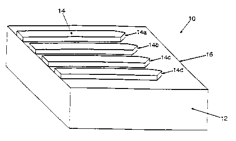
Figure 3 shows a wafer 10, for example a section of a semiconductor wafer, in
inter-
mediate state of fabrication. It shows a surface 16 of a substrate 12 covered
by a
support layer 14, being electrically isolating, such as silicon oxide. The
deposition of
the support layer 14 can be accomplished by any technique known in the art,
such as
chemical vapour deposition (CVD), plasma enhanced CVD (PECVD), electron cyclo-
tron resonance (ECR) or sputtering. As shown in figure 3, the support layer 14
is
patterned and etched to form beams with tapered end-points 14a-d. The beams
are
not limited to any particular form or symmetry; they can be of any geometry
with
suitable end-points.
The pattern is formed by forming a photoresist pattern (not shown in figure 3)
which
defines the four beams on the top surface of the support layer 14. The
photoresist
CA 02381803 2002-02-11
WO 01/20347 PCT/DK00/00513
23
pattern is formed by conventional photolithographic photoresist formation,
exposure,
development and removal techniques. The support layer is then etched using any
technique known in the art, such as dry etching or wet etching, until the
unmasked
parts of the support layer 14 are removed from the top surface of the
substrate.
In an alternative embodiment of the present invention the four beams or part
of them
can be defined using high-resolution lithographic methods such as electron-
beam
lithography, atomic force microscopy (AFM) lithography or laser lithography.
Once the support layer has been patterned, the substrate is partially removed
to
release the patterned support layer, forming four cantilevers with sharpened
end-
points 14a-d, as illustrated in figure 4.
In the preferred embodiment, the substrate is removed by depositing a
protective layer
(not shown in figure 4) of silicon nitride on top and bottom surface of the
substrate 12.
Next, a photoresist pattern is formed on the bottom surface of the substrate
by con-
ventional photolithographic photoresist formation, exposure, development and
removal
techniques. The nitride layer is then removed in the unmasked areas on the
bottom
surface of the substrate using Reactive Ion Etch (RIE) in a plasma containing
SF6 and
OZ or similar reagents, and the substrate is etched using an etching chemistry
com-
prising potassium hydroxide (KOH) or a similar chemistry until the freely
extending
probe arms are exposed. Then the protecting layer of nitride is removed from
the top
surface of the substrate using RIE, or using wet etching with a chemistry
comprising
phosphoric acid (H3P04) or a similar chemistry.
Figure 5, illustrates the etching of the substrate 12 to undercut the support
layer 14. In
the preferred embodiment, this etching step is performed with a dry etching
method,
such as an isotropic RIE etch.
The final stage of fabrication is shown in figure 6, and involves the
deposition of an
electrically conducting layer 18 on the top surface of the wafer. The
conducting layer is
made of conducting materials like Au, Ag, Pt, Ni, Ta, Ti, Cr, Cu, Os, W, Mo,
Ir, Pd, Cd,
Re, conductive diamond, metal silicides or combinations thereof. Alternatively
the con-
ducting layer can be made of a highly doped semiconducting material. The
conducting
layer can be deposited using electron-beam evaporation, or any other similar
tech-
nique known in the art. Due to the undercutting of the support layer 14, the
electrically
CA 02381803 2002-02-11
WO 01/20347 PCT/DK00/00513
24
conducting layer will not create conducting paths between the four beams made
in the
support layer, and thus four isolated electrodes are formed on the top surface
of the
support beams, and thus points 18a-d can be connected through the beams to an
external positioning and measuring device (not shown in figure 6).
As shown in figure 6 the deposition of the conducting layer creates electrodes
on the
substrate. In a preferred embodiment these electrodes are used for active
guarding of
the conductive probe arms to significantly reduce leakage resistance and,
conse-
quently, increase the measuring accuracy of the invention.
Referring again to figure 6, in the present invention the minimum probe end-
point
separation s is approximately 1 Vim. The minimum probe end-point separation is
how-
ever determined by the current state of the art in micro-fabrication
technology and not
any limitation of the present invention. Thus, as micro-fabrication technology
produces
smaller and smaller devices, the minimum probe end-point separation s can also
be
reduced.
In operation an external positioning device places a multi-point probe made
according
to the present invention into physical contact with the surface of the test
sample. Once
electrical contact between the surface of the test sample and all four
conductive probe
arms has been achieved, a current is applied to two of the conductive probe
arms and
a corresponding voltage is measured between the two other conductive arms. The
method for applying the current and detecting the voltage can be any method
known in
the art.
The preferred embodiment of the multi-point testing apparatus of the present
invention
is shown in figure 7. The figure depicts a multi-point testing apparatus 100,
a test
sample 110 is mounted on a stage 112 with an XYZ positioning mechanism. This
mechanism can be controlled automatically or manually. A multi-point probe
made ac-
cording to present invention 102 is mounted above the surface of the test
sample on a
probe holder 104 which can be moved in the Z direction with a resolution of
0.1 pm or
better. Optionally the probe holder 104 can be controlled with similar spatial
resolution
in the X and Y directions. The set-up 100 is similar to that of an AFM or a
Scanning
Tunnelling Microscope (STM). Connections 114 from the probe end-points are
input to
a controller 106, which can move the multi-point probe with respect to the
test sample
110. Optionally a connection 116 from the test sample 110 can also be input to
the
CA 02381803 2002-02-11
WO 01/20347 PCT/DK00/00513
controller 106. The controller 106 can be a computer or a programmed micro-con-
troller. By monitoring the four point resistance using the end-points of the
four probe
arms or the two point resistances between the end-points of the four probe
arms and
the test sample 110, the controller 106 can move the multi-point probe towards
the test
5 sample until all end-points of the four probe arms are in physical contact
with the test
sample. By holding the multi-point probe having the probe arm lengths in an
angle
relative to the surface of the test sample 110, smaller than perpendicular and
larger
than parallel, full individual probe arm flexibility is achieved, providing a
safe mode of
operation in regards to avoiding destruction of single devices on top surface
of test
10 sample. Then a measurement can be made of the test sample resistivity, and
the con-
troller 106 analyses the measured data and displays measurement information on
dis-
play 108. The controller 106 may retract the multi-point probe, move the test
sample
110 in the XY plane and repeat the procedure.
15 Figure 8 illustrates a similar apparatus 200 where the test sample stage
consists of a
XY positioned 222 on a standard optical microscope 214. A multi-point probe
made in
accordance to the present invention 202 is placed on a probe holder 204, which
is
mounted on a microscope objective 212, allowing the operator to identify
features on
the test sample surface and perform four point probe measurements at these
features.
20 In this manner ~m sized test sample features such as single microelectronic
devices or
polycrystalline grains can be probed in a controlled fashion. Similar to the
previously
described apparatus 100, illustrated in figure 7, the four leads 218 from the
probe are
input to a controller 206 as well as a lead 216 connecting to the test sample;
the con-
troller outputs signals 220 controlling the movement of the probe holder, and
the con-
25 troller 206 analyses and presents the measurement data on display 208.
Figure 9, pictures a detachable multi-point probe in a semi-conducting wafer.
A wafer
can consist of several multi-point probes, which are detachable from the
wafer. This
production technique provides an extremely repeatable and safe method of
fabrication
of multi-point probes.
Figure 10, shows a principal diagram of the circuit used for performing
measurements,
comprising an electrometer and a current source. Applying integrated circuit
tech-
niques for the fabrication of multi-point probes enables the possible
integration of the
electrometer, current source and additional circuit on the wafer.
CA 02381803 2002-02-11
WO 01/20347 PCT/DK00/00513
26
A particular preferred embodiment of the present invention utilises electron
beam
deposition techniques for growing tips on probe arms. Figure 11 (a), shows
such an
electron beam deposition grown from a surface 1105 of a probe arm having the
elec-
tron beam 1103 in a perpendicular relation to the surface thus creating a
primary tip
1101 having an axis perpendicular to surface plane. By tilting an electron
beam 1115
in relation to a surface 1113 a tilted electron beam deposition grows either
on the sur-
face 1113 of substrate as a primary tip 1111 or as a secondary tip 1109 in
continuation
on top of a previously produced tip 1107 perpendicular to the surface 1113.
The electric properties of the tips may be modified by applying contaminants
1203 to a
tip 1201 utilising an injection of metallo-organic compound at low partial
pressure,
hereby obtaining tips with resistances as low as 900 S2 (in-situ
metallization). The
electric properties of the tips may also be modified by applying a metallic
cloud or
evaporation 1209 creating metallic layers 1205,1207 on the tip 1201 and on the
sur-
face 1105 subsequent to finalising the tip growth (ex-situ metallization). By
applying
subsequent evaporations 1209 using two or more application angles a good
metallic
coverage of the tip 1101 and the surface 1105 are achieved, thus providing
useful tips
1101. Figure 12, shows both methods for metallization of tips.
The geometry of a probe is shown in Figure 13 in top view, side view and front
view.
The probe is shown having to probe arms 1301 on to which primary tips 1303
have
been grown by utilising electron beam deposition. The primary tips 1303 create
an
angle 1307 (a1) between direction of axial length of the probe arm 1301 and
direction
of axial length of primary tips 1303. Secondary tips 1305 extend from the
primary tips
1303 on the probe arms 1301. The primary tips 1303 furthermore have an
inclination
1309 (~1 ) and the secondary tip 1305 and additional inclination 1311 (~2) in
relation to
the direction of the axial length of the probe arm 1301.
Several tip configurations are shown in figure 14. Figure 14 (a) shows four
parallel
probe arms, two outer probe arms 1401 and the two inner probe arms 1301 having
two primary tips 1303 positioned on the two inner probe arms 1301. The two
primary
tips 1303 create an angle in relation to axial direction of the inner probe
arms 1301
such that the primary tips 1303 point a common orientation. Figure 14 (b)
shows the
four parallel probe arms 1301,1401 having four primary tips 1303,1403
positioned so
that the end point have equal tip separations. Figure 14 (c) shows the four
probe arms
1301,1401 each having primary tips 1303,1403 extending from distal end. The
two
CA 02381803 2002-02-11
WO 01/20347 PCT/DK00/00513
27
inner probe arms 1301 having the primary tips 1303 pointing toward a common
orien-
tation and the two outer probe arms 1401 pointing toward in axial direction of
the outer
probe arms 1401. Figures 14 (d) to (f) show secondary tips 1305,1405 added to
the
primary tips 1303,1403.
The fabrication scheme for producing primary and secondary tips applying
electron
beam deposition is shown in figure 15. Figure 15 (a) shows the two probe arms
1301
having distal ends defined as 1501 and 1505. The electron beam is aimed at a
corner
1503 of the surface of the distal end 1505, hereby producing the primary tip
1303. As
shown in figure 15 (b) the electron beam is subsequently aimed at a corner
1507 of
the surface of the distal end 1501, hereby producing the second primary tip
1301. This
procedure is repeated until the separation between the two primary tips 1301
is slightly
larger than the intended gap G' between the primary tips 1301. The primary
tips 1303
create an angle in relation to axial direction of probe arms 1301 and an angle
in rela-
tion to the surfaces of the distal ends 1501,1505 such that the primary tips
1303 point
away from the supporting body of the multi-point probe. The secondary tips
1305
furthermore create an angle in relation to axial direction of the primary tips
1303. In
order to achieve this secondary angling of the secondary tips 1305 in relation
to the
primary tips 1301 the multi-point probe is rotated as shown in figure 15(e).
Figure 16, shows electron microscope pictures of the fabrication scheme
presented
above and in figure 15.
As shown in figure 18a, a preferred embodiment of the cylindrical nano-drive
includes
a cylindrical movable member 1803 movably supported in a surrounding substrate
1801. An electro-mechanical actuator 1805 is fixed on the movable member,
and an inertial member 1807 is fixed in the distal end of said actuator. A
distributed
intrinsic frictional force exists between the movable member and the support.
This fric-
tional force originates from the internal elastic forces of the movable member
and the
support, and appears because of a high-precision machining of the movable mem-
ber and the support. In a preferred embodiment, the support and the movable
member is machined to fit within a tolerance of the diameter of less than one
micro-
meter. This fit can be performed using milling, drilling, etching, honing,
polishing,
lapping, or any other known technique for machining of materials. In a
preferred
embodiment the movable member and the support consists of chemically inert,
hard
materials such as semiconductor carbides or nitrides. The electro-mechanical
actu-
CA 02381803 2002-02-11
WO 01/20347 PCT/DK00/00513
28
ator has at least two electrodes to allow it to be moved in a direction
parallel with the
travel of the movable member. In a preferred embodiment the electro-mechanical
actuator is a piezoelectric tube with one inner electrode and four outer
electrodes, to
provide both transverse and longitudinal motion of the actuator and thus of
the inertial
member.
In a second embodiment, the movable member in the cylindrical nano-drive
according to the invention is a hollow tube which is closed in one end, as
shown in
figure 18b. The electro-mechanical actuator is fixed to the bottom of the
tube.
In a third embodiment, the movable member in the cylindrical nano-drive
according to
the invention is a hollow tube which is closed in one end, and is movably
supported on
the inside of the tube as shown in figure 18c.
Figure 19a shows an embodiment of a micro-pipette 1901 according to the
invention.
The micro-pipette consists of a cylindrical nano-drive according to the
invention,
which has a movable member 1907 movably supported inside a tube 1903, said
tube having an opening 1913 through which very small amounts of liquid or gas
can be
dispensed or acquired. An electro-mechanical actuator 1909 is fixed to the
movable member, and an inertial member 1911 is fixed to the distal end of the
actuator. The position of the movable member is controlled by electrical
signals
applied to the electro-mechanical actuator in such a way that the volume of
gas or
liquid in the tube is controlled with very high accuracy. Figure 19b shows a
sectional
view of the micro-pipette.
Figure 20a shows an embodiment of a micro-valve 2001 according to the
invention.
The micro-valve consists of a cylindrical nano-drive according to the
invention,
which has a movable member 2007 movably supported inside a tube 2003 which
has two openings through which a gas or liquid 2005 is flowing. The movable
member
can completely or in part block said flow by applying electrical signals to
the
electro-mechanical actuator 2009 which is fixed to the movable member, and
thus
the flow can be controlled with a very high degree of accuracy. Figure 20b
shows a
sectional view of the micro-valve.
Figure 21 a shows an embodiment of a nano-positioner 2101 according to the
invention. The nano-positioner consists of a cylindrical nano-drive according
to the
CA 02381803 2002-02-11
WO 01/20347 PCT/DK00/00513
29
invention with a movable member movably supported by a tubular substrate 2103.
The position of the substrate can be changed by applying electrical signals to
the
electro-mechanical actuator 2105. In the distal end of the actuator is fixed a
probe 2109 which is also the inertial member of the cylindrical nano-drive.
The
probe can be moved in all directions relative to a material 2111 by applying
electrical signals to the electro-mechanical actuator. Figure 21 b shows a sec-
tional view of the nano-positioner. Figure 21 c shows an alternative embodi-
ment of the nano-positioner where the movable member has two actuators fixed
at
opposing sides. The additional actuator 2107 has an inertial member 2113 fixed
at the
distal end. The actuator 2113 can be controlled independent of the actuator
2105
which allows the probe to be move continuously over distances of millimeter in
the
direction of movement of the movable member relative to the material. The
electrical
fields necessary to achieve this are shown schematically in figures 23a-b. A
saw-
tooth-like waveform is applied to one of the actuators, while a similar
waveform
of opposing sign is applied to the other actuator. By fine-tuning of the
amplitude and
phase of the two waveforms, a continuous movement of the probe will appear.
Figures 22a-c shows curve-forms for electrical signals to control the movement
of the movable member in a cylindrical nano-drive according to the invention
in which
the actuator can be moved in both transverse and longitudinal directions. The
longitudinal movement of the actuator is controlled by a harmonic oscillating
signal as shown in figure 22a. When one or both transverse movements are dri-
ven by a harmonic oscillating electrical signal with half the frequency of the
longitudinal
signal, and when all extrema on the transverse signal coincide with either
maxima or
minima in the longitudinal signal, then the movable member will be displaced
either
up or down. These curve-forms are shown in figures 22b-c. By changing the
amplitude and the frequency of the harmonic signals, the movement of the
movable
member per period of the harmonic signal can be made arbitrarily small.
Figure 24 shows schematically a complete micro-pipette apparatus 2401
according to
the invention. The micro-pipette is constructed as described above with
reference to
figure 19, with the movable member 2405 movably supported inside a tube 2403
which is tapered into a pipette tip 2423. On the movable member is fixed an
electro-mechanical actuator 2407 which has an inertial member 2409 fixed to
the distal end. The electrodes on the electro-mechanical actuator are
connected
to a control-box 2411 through amplifiers 2417 - 2421 with electrical wires
2415. The
CA 02381803 2002-02-11
WO 01/20347 PCT/DK00/00513
control box can include a computer, a microprocessor or discrete digital or
analog
components. The control box can be controlled remotely by a computer or with a
panel 2413 on which the speed and direction of the movable member can be
selected.
5 In a more advanced embodiment of the micro-pipette apparatus, the micro-
pipette is attached to a manual or motorized stage, in such a way that the
micro-pipette tip can be moved relative to the media in which gas or liquid is
to be
dispensed or extracted. In the case of an motorized stage, an automatic micro-
pipette system is realized, in which the micro-pipette and perform movements
10 synchronized with dispensing or extracting fluid or gas.
Figure 25 shows schematically a complete micro-valve apparatus 2501 according
to
the invention. The micro-valve is constructed as described above with
reference to
figure 20, with a movable member 2505 movably supported inside a tube 2503 in
15 which a transverse flow of gas or liquid 2513 is present. On the movable
member is
fixed an electro-mechanical actuator 2507 which has an inertial member 2509
fixed to
the distal end. The electrodes on the electro-mechanical actuator are
connected to a
control-box 2511 through amplifiers 2517 - 2521 with electrical wires 2515.
The
control box can include a computer, a microprocessor or discrete digital or
analog
20 electronic components.
Figure 26a shows schematically a complete nano-positioner apparatus 2601
according to the invention. The nano-positioner apparatus is constructed from
an
embodiment of the cylindrical nano-drive according to the invention in which
the
25 inertial member 2609 comprises a microscopic probe, for example a very
sharp elec-
trode. The nano-positioner apparatus can move the probe relative to a sample
2611.
An electrical connection 2619 from the probe can be sent though an amplifier
2617 to
a control box 2613. An electrical connection 2621 can also be made between the
sample and the control box. The control box contains a feedback system which
uses
30 the electrical signal from the microscopic probe to adjust the position of
the micro-
scopic probe relative to the sample. The position of the probe is controlled
by at least
one electrical connection 2623 between the control box and the electro-
mechanical
actuator 2607 on the movable member 2605 of the cylindrical nano-drive, which
is
movably supported in a surrounding substrate 2603. The electrical signal to
the actu-
ator can pass through an amplifier 2625 - 2629. In a preferred embodiment the
actuator comprises a piezoelectric tube with electrodes allowing transversal
and
CA 02381803 2002-02-11
WO 01/20347 PCT/DK00/00513
31
longitudinal movement of the microscopic probe with respect to the sample. In
this
way a scan of the sample material can be obtained as a function of position,
and the
obtained data can be presented on a display 2615 connected to the control box.
Figure 26b shows an alternative embodiment of the nano-positioner apparatus,
further
comprising a second electro-mechanical actuator 730 fixed to the movable
member of
the cylindrical nano-drive according to the invention. A inertial member 732
is fixed to
the distal end of the electro-mechanical actuator. There is at least one
electrical
connection 2631 between the second electro-mechanical actuator and the control
box. The electrical signal can pass though an amplifier 2633 - 2637.
Example showing the usage of the multi-point probe.
The probe chips (illustrated in figure 9) are broken out of the wafers and are
mounted
on ceramic dies (5mm x 10mm) with four big thick-film electrode pads, using
epoxy.
The conductive probe arms on the silicon chips are connected to the pads on
the
ceramic dies by bonding 25~,m thick gold wires between them, using a Kulicke-
Soffa
wedge-bonding machine.
The ceramic chips are fixed mechanically and contacted electrically on an
aluminium
mount, which is machined to fit around a microscope objective on a Karl-Suss
probe
station. The mount allows the conductive probe arms of the multi-point probe
to be in
focus in the middle of the field of view of the microscope. The test sample
can then be
moved into focus using the normal vertical stage of the microscope. When the
test
sample is in focus the multi-point probe will contact the test sample and a
measure
ment can be performed. This set-up is similar to the general illustration in
figure 8.
Electronics consisting of an electrometer and a current source is built into
the alumin-
ium mount to minimise the distance between the probe and the electronics. This
keeps
the noise in the measurements at a minimum. The principal diagram of the
circuit is
shown in figure 10. The two inner conductive probe arms of the multi-point
probe are
connected to an electrometer (an instrumentation amplifier) with an input
impedance of
more than 10GS2 and an amplification factor of 5000. The peripheral two
conductive
probe arms of the probe are connected to the current source (a differential
voltage to
current converter) which delivers an adjustable output in the range of 10nA to
1 E.~A.
CA 02381803 2002-02-11
WO 01/20347 PCT/DK00/00513
32
The current output is proportional to the voltage difference V1-V2. These
voltages are
generated externally by a computer equipped with a digital to analogue
converter. The
same computer detects the output voltage Vo of the electrometer through an
attached
analogue to digital converter. Batteries power the circuit in order to make it
float with
respect to ground.
A measurement is performed by sampling the voltage of the electrometer for
both
polarities of the current, taking the average of the two values. This
averaging pro-
cedure is useful for eliminating thermal drift in the electronics.
Essential features of the invention represented by following points.
1. A multi-point probe for testing electric properties on a specific location
of a test
sample, comprising:
(a) a supporting body defining a first surface;
(b) a first multitude of conductive probe arms each of said conductive probe
arms
defining a proximal end and a distal end being positioned in co-planar
relationship
with said first surface of said supporting body, and said conductive probe
arms
being connected to said supporting body at said proximal ends thereof and
having
said distal ends freely extending from said supporting body, giving
individually
flexible motion to said first multitude of conductive probe arms; and
(c) said conducting probe arms originating from a process of producing said
multi-
point probe including producing said conductive probe arms on supporting wafer
body in facial contact with said supporting wafer body and removal of a part
of said
wafer body providing said supporting body and providing said conductive probe
arms freely extending from said supporting body.
2. The multi-point probe according to point 1, wherein said first multitude of
conduc-
tive probe arms are unidirectional, constituting a first multitude of parallel
free ex-
tensions of said supporting body.
3. The multi-point probe according to points 1 and 2, wherein said supporting
body
further comprising a second surface parallel to said first surface and said
multi-
point probe further comprising an additional multitude of conductive probe
arms
defining a proximal end and a distal end being positioned in co-planar
relationship
with said second surface of said supporting body, and said additional
conductive
CA 02381803 2002-02-11
WO 01/20347 PCT/DK00/00513
33
probe arms being connected to said supporting body at said proximal ends
thereof
and having said distal ends freely extending from said supporting body, giving
individually flexible motion to said additional multitude of conductive probe
arms.
4. The multi-point probe according to points 1-3, wherein said first multitude
of con-
ductive probe arms are in a multiple of 2, ranging from at least 2 said
conductive
probe arms to 64 said conductive probe arms, preferable application having 4
said
conductive probe arms.
5. The multi-point probe according to points 1-4, wherein said first multitude
of con-
ductive probe arms have a substantially rectangular cross section defining:
the
dimension of width as a distance between the lines of said rectangular cross
sec-
tion perpendicular to the plane of said first surface of said supporting body,
the
dimension of depth as a distance between the lines of said rectangular cross
sec-
tion parallel to the plane of said first surface of supporting body, and the
dimension
of length as a distance from said proximal end of said conductive probe arms
to
said distal end of said conductive probe arm.
6. The multi-point probe according to points 1-5, wherein said first multitude
of con-
ductive probe arms have a ratio of said length to said width within the range
of
500:1 to 5:1, such as ratios 50:1 and 10:1, preferable application having the
ratio of
10:1.
7. The multi-point probe according to points 1-6, wherein said first multitude
of con-
ductive probe arms have a ratio of said width to said depth within the range
of 20:1
to 2:1, preferable application having the ratio of 10:1.
8. The multi-point probe according to points 1-7, wherein said first multitude
of con-
ductive probe arms has tapered elements extending from said distal end of said
conductive probe arms.
9. The multi-point probe according to points 1-7, wherein said first multitude
of con-
ductive probe arms has pointed shaped elements extending from said distal end
of
said conductive probe arms.
CA 02381803 2002-02-11
WO 01/20347 PCT/DK00/00513
34
10. The multi-point probe according to points 1-7, wherein said first
multitude of con-
ductive probe arms has enlarged circular, elliptic or orthogonal squared
elements
extending form said distal ends of said conductive probe arms.
11. The multi-point probe according to points 1-10, wherein said first
multitude of con-
ductive probe arms have said lengths in the range of 20pm to 2mm, preferably a
length of 200pm.
12. The multi-point probe according to points 1-11, wherein said first
multitude of con-
ductive probe arms have a separation of distal ends of said conductive probe
arms
in the range of 1 ~m to 1 mm, preferable application having said separations
of
20~m, 40~m and 60ym.
13. The multi-point probe according to points 1-12, further comprising a
second multi-
tude of conductive electrodes being position on second multitude of areas
defined
on said first surface between said first multitude of conductive probe arms,
and
comprising an insulating spacing between said electrodes and said conductive
probe arms, said second multitude of conductive electrodes especially being
suitable for active guarding.
14. The multi-point probe according to point 13, wherein said second multitude
of
areas are swaged in relation to the plane of said first surface of said
supporting
body.
15. The multi-point probe according to point 13, wherein said second multitude
of
areas are elevated in relation to the plane of said first surface of said
supporting
body.
16. The multi-point probe according to point 13, wherein said second multitude
of
areas are in co-planar relation with said first surface of said supporting
body
between said first multitude of conductive probe arms.
17. The multi-point probe according to points 13-16, wherein said second
multitude of
areas are combinations of swaged, elevated and co-planar in relation to the
plane
of said first surface of said supporting body.
CA 02381803 2002-02-11
WO 01/20347 PCT/DK00/00513
18. The multi-point probe according to points 13 and 17, wherein said second
multi-
tude of swaged areas undercut said first multitude of conductive probe arms on
said supporting body providing a supporting surface of said supporting body
smaller than the surface of said conductive probe arms facing said supporting
5 body.
19. The multi-point probe according to points 13, 17 and 18, wherein said
second
multitude of swaged areas undercutting said first multitude of conductive
probe
arms are originating from a process of producing said multi-point probe
including
10 producing said conductive probe arms on supporting wafer body in facial
contact
with said supporting wafer body and removal of a part of said wafer body
providing
said second multitude of swaged areas on said supporting body by a process of
chemical vapour deposition (CVD), plasma enhanced CVD (PECVD), electron
cyclotron resonance (ECR) or sputtering, mechanical grinding, etching, high
15 resolution lithographic methods such as electron-beam lithography, atomic
force
microscopy (AFM) lithography or laser lithography.
20. The multi-point probe according to points 1-19, wherein supporting body is
of a
ceramic material.
21. The multi-point probe according to points 1-19, wherein supporting body is
of a
semiconducting material.
22. The multi-point probe according to point 21, wherein said semiconducting
material
comprising Ge, Si or any combinations thereof.
23. The multi-point probe according to points 20-22, comprising:
(a) a conductive layer positioned on said multitude of conductive probe arms;
and
(b) a conductive layer acting as said electrodes on said supporting body
between
said first multitude of conductive probe arms.
24. The multi-point probe according to point 23, wherein said conductive layer
com-
prising conductive materials such as Au, Ag, Pt, Ni, Ta, Ti, Cr, Cu, Os, W,
Mo, Ir,
Pd, Cd, Re, conductive diamond, metal silicides or any combinations thereof.
CA 02381803 2002-02-11
WO 01/20347 PCT/DK00/00513
36
25. The multi-point probe according to points 1-24, wherein said multi-point
probe
further comprising:
(d) a third multitude of conductive tip elements extending from said distal
end of
said first multitude of conductive probe arms; and
(e) said conductive tip elements originating from a process of metallization
of
electron beam depositions on said first multitude of conductive probe arms at
said distal ends thereof.
26. The multi-point probe according to point 25, wherein each of said third
multitude of
conductive tip elements comprises a primary section and a secondary section,
said
conductive tip elements being connected to said conductive probe arms through
respective primary sections thereof and said secondary sections defining free
contacting ends.
27. The multi-point probe according to points 25 or 26, wherein each of said
primary
sections defines a first axial direction, said first axial direction
constituting an in-
crease of the total distance between said supporting body and said free
contacting
ends.
28. The multi-point probe according to point 27, wherein said first axial
direction of said
primary section constitutes a decrease of separation between said free
contacting
ends of said third multitude of conductive tip elements.
29. The multi-point probe according to points 27-28, wherein said first axial
direction of
said primary section constitutes a decrease of separation between adjacent
said
free contacting ends of said third multitude of conductive tip elements.
30. The multi-point probe according to points 25-29, wherein each of said
secondary
sections defines a second axial direction, said second axial direction
constituting
an increase of the total distance between said supporting body and said free
contacting ends.
31. The multi-point probe according to point 30, wherein said second axial
direction of
said secondary section constitutes a decrease of separation between said free
contacting ends of said third multitude of conductive tip elements.
CA 02381803 2002-02-11
WO 01/20347 PCT/DK00/00513
37
32. The multi-point probe according to points 30-31, wherein said secondary
axial
direction of said secondary section constitutes a decrease of separation
between
adjacent said free contacting ends of said third multitude of conductive tip
elements.
33. The multi-point probe according to points 27-32, wherein said first axial
direction of
said primary sections extend parallel to the plane defined by said first
surface of
said supporting body.
34. The multi-point probe according to points 27-32, wherein said first axial
direction of
said primary sections extend in a direction converging towards the plane
defined
by said second surface of said supporting body.
35. The multi-point probe according to points 30-34, wherein said second axial
direc-
tion of said secondary sections extend parallel to the plane defined by said
first
surface of said supporting body.
36. The multi-point probe according to points 30-34, wherein said second axial
direc-
tion of said secondary sections extend in a direction converging towards the
plane
defined by said second surface of said supporting body.
37. The multi-point probe according to points 25-36, wherein said third
multitude of
conductive tip elements is equal to said first multitude of conductive probe
arms,
preferable application having third multitude dividable with 2.
38. The multi-point probe according to points 25-36, wherein said third
multitude of
conductive tip elements is less than said first multitude of conductive probe
arms,
preferable application having third multitude dividable with 2.
39. The multi-point probe according to points 25-36, wherein said third
multitude of
conductive tip elements is greater than said first multitude of conductive
probe
arms, preferable application having third multitude dividable with 2.
40. The multi-point probe according to points 25-39, wherein said third
multitude of
conductive tip elements have a separation of said free contacting ends of said
CA 02381803 2002-02-11
WO 01/20347 PCT/DK00/00513
38
conductive tip elements in the range of 1 nm - 100 nm, preferable application
having said separations of 2 nm, 5 nm, 10 nm, 20 nm, 50 nm, 100 nm.
41. The multi-point probe according to points 25-40, wherein each of said
conductive
tip elements define an overall length as distance between said distal ends of
conductive probe arms and said free contacting ends of said conductive tip
elements, said overall length being in the range of 100 nm to 100 Vim,
preferable
application having said overall length in the ranges 500 nm to 50 pm and 1 pm
to
Vim.
42. The multi-point probe according to points 25-41, wherein each of said
conductive
tip elements define a diameter, said diameter being in the range of 10 nm to 1
Vim,
preferable application having said overall length in the ranges 50 nm to 500
nm.
43. The multi-point probe according to points 25-42, wherein said third
multitude of
conductive tip elements mainly consists of carbon.
44. The multi-point probe according to points 25-43, wherein said third
multitude of
conductive tip elements further consists a concentration of contaminants.
45. The multi-point probe according to points 25-42, wherein said third
multitude of
conductive tip elements originate from a process of tilted electron beam
deposition.
46. The multi-point probe according to points 25-42, wherein said third
multitude of
conductive tip elements originate from a process of perpendicular electron
beam
deposition.
47. The multi-point probe according to points 25-42, wherein said third
multitude of
conductive tip elements originate from a process of a combination of tilted
electron
beam deposition and perpendicular electron beam deposition.
48. The multi-point probe according to points 25-47, wherein said
metallization of said
third multitude of conductive tip elements originates from a process of in-
situ
metallic deposition.
49. A method of producing a multi-point probe comprising the following steps:
CA 02381803 2002-02-11
WO 01/20347 PCT/DK00/00513
39
(i) producing a wafer body;
(ii) producing a first multiple of conductive probe arms positioned in co-
planar and
facial relationship with said wafer body;
(iii) removing a part of said wafer body for providing said conductive probe
arms freely
extending from said non-removed part of said wafer body constituting a
supporting
body from which said conductive probe arms extend freely; and
(iv) producing a third multitude of conductive tip elements extending from
said distal
end of said first multitude of conductive probe arms.
50. The method according to point 49, wherein the technique of applying the
con-
ductive probe arms in co-planar and facial relationship with the supporting
wafer
body, involves microfabrication technique, planar technique, CMOS technique,
thick-film technique, thin-film technique or a combination thereof.
51. The method according to points 49 and 50, wherein the technique of
applying the
third multitude of conductive tip elements extending from said distal end of
said
first multitude of conductive probe arms, involves metallization of electron
beam
depositions.
52. The method according to points 49-51, wherein said producing of said third
multi-
tude of conductive tip elements comprising steps:
(a) mounting of multi-point probe having said first surface of supporting body
parallel to horizontal on to holding means in a microscope chamber;
(b) selecting angles a and ~ describing inclination of said primary section
and said
secondary section of said conductive tip elements;
(c) measuring of deposition rate by focusing an electron beam in one location
for 5
minutes and measuring the resulting length of a first deposition;
(d) tilting and rotating said holding means to give a field of view of said
first
deposition from an viewing angle identical to angle of said electron beam
showing accordance with said selected angles a and Vii;
(e) depositing a length on one of said distal ends of said conductive probe
arms;
(f) tilting and rotating said holding means to give a field of view of
position for a
second deposition;
(g) depositing said length on neighbouring said distal end of said conductive
probe
arms;
CA 02381803 2002-02-11
WO 01/20347 PCT/DK00/00513
(h) repeating steps c through g until separation of conductive probe arms is
approximately 100 nm greater than the indented separation of conductive
probe arms;
(i) selecting an angle a1 describing a inclination of said secondary section;
5 Q) tilting and rotating said holding means selecting ~=0 and selecting an
a=a1;
(k) extending said secondary sections in continuation of said primary
sections; and
(I) ensuring that the depositing progresses by alternating the position of the
electron beam on first and second deposition.
10 53. The method according to points 49-52, the multi-point probe having any
of the
features of the multi-point probe according to any of the points 1-48.
54. A cylindrical nano-drive for in particular driving tools with high
resolution and com-
prising
15 a supporting body defining an inner open ended cylindrical space having a
first longitudinal axis and an inner cylindrical surface,
a movable member defining an outer contact surface, a first mounting surface
and a second mounting surface, said outer contact surface mating said inner
open
ended cylindrical space, said movable member being inserted into said inner
open
20 ended cylindrical space and said contacting surface of said movable member
and
said inner cylindrical surface of said inner open ended cylindrical space
creating a
sliding fit between said movable member and said supporting body,
said sliding fit between said movable member and said supporting body being
established along the entire area of contact between said inner cylindrical
surface
25 and said outer contact surface and being provided by said outer contact
surface
and said inner cylindrical surface defining therebetween a spacing of a
dimension
having a size at any specific area of said area of contact of no more than 1
to 5
orders of power of atomic dimensions, preferably 1 to 3, 3 to 5 or 2 to 4,
an inertial body having a first proximal end and second proximal end and
30 providing counter weight for said movable member, and
an actuator defining a second longitudinal axis, a third proximal end and a
fourth proximal end, said actuator being connected at said third proximal end
to
said first proximal end of said inertial body and said fourth proximal end of
said
actuator being connected to said first mounting surface of said movable
member,
35 said second longitudinal axis of said actuator being substantially parallel
to said
first longitudinal axis of said open ended cylindrical space,
CA 02381803 2002-02-11
WO 01/20347 PCT/DK00/00513
41
said actuator moving said movable member in said cylindrical space by con-
traction and extension of said actuator in a direction parallel to said first
longi-
tudinal axis.
55. The cylindrical nano-drive according to point 54, wherein said supporting
body is
constructed from chemically inert and hard materials such as carbides and
nitrides.
56. The cylindrical nano-drive according to point 54 or 55, wherein said
supporting
body defining an overall triangular, rectangular, elliptical, conical,
cubical, spherical
or cylindrical outer surface or any combinations thereof, preferably said
supporting
body defining an overall cylindrical outer surface.
57. The cylindrical nano-drive according to point 56, wherein said cylindrical
outer sur-
face of said supporting body defines a third longitudinal axis substantially
coaxial
with said first longitudinal axis.
58. The cylindrical nano-drive according to points 54 to 57, wherein said
inner open
ended cylindrical space defines a circular cross sectional area having an
inner
diameter.
59. The cylindrical nano-drive according to any of the points 54 to 58,
wherein said
movable member is constructed from chemically inert and hard materials such as
carbides and nitrides.
60. The cylindrical nano-drive according to any of the points 54 to 59,
wherein said
movable member defining an overall triangular, rectangular, elliptic, cubical,
spheri-
cal, conical or cylindrical outer shape or any combinations thereof,
preferably said
movable member defining an overall solid cylindrical shape defining said first
mounting surface at one end of said solid cylindrical shape and said second
mounting surface at the other end of said cylindri-:al shape, said said first
and said
second mounting surface defining a circular area having an outer diameter sub-
stantially equal to said inner diameter of said open ended cylindrical
surface, so as
to provide a sliding fit between said movable member and said supporting body.
61. The cylindrical nano-drive according to any of the points 54 to 59,
wherein said
movable member defining an overall cylindrical cup shape having an outer
CA 02381803 2002-02-11
WO 01/20347 PCT/DK00/00513
42
diameter substantially equal to said inner diameter of said open ended
cylindrical
surface constituting a sliding fit between said movable member and said inner
cylindrical surface of said supporting body and defining a bottom inner cup
surface
constituting said first mounting surface and a bottom outer cup surface
constituting
said second mounting surface and having said fourth proximal end of said
actuator
mounted to said first mounting surface with said second longitudinal axis of
said
actuator being substantially parallel to said first longitudinal axis of said
open
ended cylindrical space.
62. The cylindrical nano-drive according to any of the points 54 to 59,
wherein said
movable member defining an overall cylindrical cup shape having an inner di-
ameter substantially equal to said outer diameter of said cylindrical surface
of said
supporting body constituting a sliding fit between said movable member and
said
cylindrical surface of said supporting body and defining a bottom outer cup
surface
constituting said first mounting surface and a bottom inner cup surface
constituting
said second mounting surface and having said fourth proximal end of said
actuator
mounted to said first mounting surface with said second longitudinal axis of
said
actuator being substantially parallel to said first longitudinal axis of said
open
ended cylindrical space.
63. The cylindrical nano-drive according to any of the points 54 to 62,
wherein said
inertial body is constructed from materials such as chemically inert and hard
materials such as carbides and nitrides.
64. The cylindrical nano-drive according to any of the points 54 to 63,
wherein said
inertial body defining an overall cubical, conical, triangular, rectangular,
elliptic,
spherical or cylindrical outer shape or any combinations thereof, preferably
said
inertial body defining an overall cylindrical shape having a third
longitudinal axis
connected at said first proximal end to said third proximal of said actuator
having
said third longitudinal axis and said first longitudinal axis substantially co-
axial.
65. The cylindrical nano-drive according to any of the points 54 to 64,
wherein said
inertial body further comprising probing means.
66. The cylindrical nano-drive according to any of the points 54 to 65,
wherein said
actuator defining an overall triangular, cubical, conical, rectangular,
elliptic,
CA 02381803 2002-02-11
WO 01/20347 PCT/DK00/00513
43
spherical or cylindrical shape or any combinations thereof preferably said
actuator
defining an overall cylindrical shape having circular cross sectional area.
67. The cylindrical nano-drive according to any of the points 54 to 66,
wherein said
actuator longitudinally and transversely contracting and extending providing a
longitudinal movement of said movable member by operating said actuator
electrically, magnetically, mechanically, hydraulically or pneumatically or
any
combinations thereof, preferably by operating said actuator electrically.
68. The cylindrical nano-drive according to any of the points 54 to 67,
wherein said
actuator is construed from piezoelectric materials such as quartz.
69. The cylindrical nano-drive according to any of the points 54 to 68,
wherein said
actuator further comprising electrodes mounted onto inner and/or outer
surfaces of
said actuator for operation of said actuator to longitudinally and
transversely
contraction and extension by applying electrical signals to said electrodes.
70. The cylindrical nano-drive according to point 69, wherein said electrical
signals are
constituted by DC signals and/or AC signals such as alternating square wave
signals, alternating triangularly shaped signals or sinusoidal signals or any
com-
binations thereof.
71. The cylindrical nano-drive according to any of the points 54 to 70,
wherein said
supporting body defining said inner cylindrical space further defines a
tapered
extension space section co-axially placed and communicating with said inner
cylindrical space and tapering toward said first longitudinal axis leaving
reduced
access through an aperture to said inner cylindrical space thereby
constituting a
micro-pipette.
72. The cylindrical nano-drive according to any of the points 54 to 71,
wherein said
supporting body defining said inner cylindrical space in communication with an
inner space comprising at least two apertures, said movable member movable
into
said inner space controlling passage between said at least two apertures
thereby
constituting a micro-valve.
73. The cylindrical nano-drive according to any of the points 54 to 72,
wherein said
CA 02381803 2002-02-11
WO 01/20347 PCT/DK00/00513
44
cylindrical nano-drive further comprising a second inertial body defining a
distal
end and a seventh proximal end and a second actuator defining a fifth proximal
end, a sixth proximal end and a fourth longitudinal axis, said fifth proximal
end of
said second actuator being connected to said seventh proximal end of said
second
inertial body and said fifth proximal end of said second actuator being
connected to
said second mounting surface of said movable member, said fourth longitudinal
axis of said second actuator being substantially parallel to said first
longitudinal
axis of said open ended cylindrical space so as to provide a substantially con-
tinuous motion of said movable member.
74. A multi-point testing apparatus for testing electric properties on a
specific location
of a test sample, comprising:
means for receiving and supporting said test sample;
electric properties testing means including electric generator means for
generating a test signal and electric measuring means for detecting a
measuring
signal;
a multi-point probe, comprising:
a supporting body;
a first multitude of conductive probe arms positioned in co-planar
relationship
with a surface of said supporting body, and freely extending from said
supporting
body, giving individually flexible motion of said first multitude of
conductive probe
arms; and
said conducting probe arms originating from a process of producing said
multi-point probe including producing said conductive probe arms on supporting
wafer body in facial contact with said supporting wafer body and removal of a
part
of said wafer body providing said supporting body and providing said
conductive
probe arms freely extending from said supporting body;
said multi-point probe communicating with said electric properties testing
means; and
nano driving means for reciprocating said multi-point probe relative said test
sample so as to cause said conductive probe arms to be contacted with said spe-
cific location of said test sample for performing said testing of electric
properties
thereof.
75. The multi-point testing apparatus according to point 74, wherein said nano-
driving
means comprises the features according to points 54 to 73.
CA 02381803 2002-02-11
WO 01/20347 PCT/DK00/00513
76. The multi-point testing apparatus according to point 74 or 75, wherein
said multi-
point probe comprises the features according to points 2 to 48.
5 77. The multi-point testing apparatus according to any of the points 74 to
76, wherein
said electric properties testing means further comprising means for electric
properties probing of said test sample.
78. The multi-point testing apparatus according to points 74 and 77, wherein
said
10 reciprocating means further comprises holding means for said means for said
multi-point probe.
79. The multi-point testing apparatus according to points 74 to 78, further
comprising
means for positioning said holding means across said test sample and recording
of
15 a location of said holding means relative to said test sample.
80. The multi-point testing apparatus according to points 74 to 79, wherein
said means
for positioning comprising manoeuvrability in all spatial directions, being
directions
co-planar to said test sample and directions perpendicular to said test
sample.
81. The multi-point testing apparatus according to points 74 to 80, wherein
said means
for positioning further comprising means for angular movement of said holding
means, such as to provide angular positions for said means for said multi-
point
probe.
82. The multi-point testing apparatus according to points 74 to 81, wherein
said means
for positioning further comprising means for angular movement of said holding
means along an axis parallel to surface of said test sample, such as to
provide
angular positions for said means for said multi-point probe.
83. The multi-point testing apparatus according to points 74 to 82, wherein
said means
for positioning further comprising means for angular movement of said holding
means along an axis perpendicular to surface of said test sample, such as to
provide angular positions for said means for said multi-point probe.
CA 02381803 2002-02-11
WO 01/20347 PCT/DK00/00513
46
84. The multi-point testing apparatus according to points 74 to 83, wherein
said means
for positioning further comprising means for sensing contact between said test
sample and said means for said multi-point probe.