Note: Descriptions are shown in the official language in which they were submitted.
CA 02381883 2002-02-13
WO 01/15820 PCT/US00/19651
ADHESIVE COATING METHOD AND ADHESIVE COATED ARTICLE
Technical Field
This invention relates to a method for making an article having an irradiated
adhesive on a radiation degradable substrate where the substrate has no
substantial
degradation. More specifically this invention relates to a drum transfer
method for
adhesive irradiation by electron beam.
Back2round
Adhesives, including pressure-sensitive adhesives, and heat activatable
adhesives
are well known in the art for bonding to a variety of materials such as
metals, painted
surfaces, plastics, and the like. Adhesives are designed to meet various
requirements by
balancing their viscous and elastic properties to result in a balance of
shear, peel, and
tack properties. Pressure-sensitive adhesives generally adhere with light
pressure and
are tacky at the use temperature. Heat activatable adhesives may adhere with
light
pressure and be slightly tacky at the use temperature, or may require elevated
temperatures or pressures to adhere to another material.
Crosslinking occurs when a polymer, that may be of a low molecular weight, is
subjected to ionizing radiation that links the polymer chains together and
increases the
effective molecular weight. Adhesives can be crosslinked to obtain the desired
balance
of properties.
Disclosure of Invention
Briefly, the present invention provides a method for making a substrate coated
with an adhesive, comprising: applying an electron beam modifiable adhesive
layer onto
a repeatably reusable transfer surface; irradiating the adhesive layer with an
electron
beam to chemically modify the adhesive layer; and transferring the irradiated
adhesive
layer to a substrate. In one embodiment, the adhesive is applied to a release
surface
before applying the adhesive to the repeatably reusable transfer surface.
In another aspect, the present invention provides an adhesive coated web,
comprising: a substrate having at least one component susceptible to electron
beam
-1-
CA 02381883 2007-06-29
60557-6657
radiation degradation seltcted from the group consisting of cellulose-based
non-woven
fabrics, ctllulose-based woven fabrics, paper, polyisobutylene films,
polypropylene films,
polypropylene-based nonwovens, polytetrafluoroethylene films, vinyl films, and
combinations thereof, having no electron beam radiation modification; and an
adhesive
layer attached to the substrate and in contact with a radiation degradable
component of
the substrate, the adhesive having an electron beam modified composition and
containing no substantial quantity of chemical, thermal, or ultraviolet
crosslinking agent.
The adhesive is selected from the group consisting of acrylics, natural
rubbers,
polybutadienes, polyisoprenes, styrene/butadiene copolymers, styrene/isoprene
copolymers, and silicones.
This invention also provides a new adhesive coated web having a substrate
having at least one component susceptible to electron beam radiation
degradation having
no electron beam radiation modification, and an adhesive layer having an
electron beam
modified composition wherein the electron beam modified adhesive layer has an
electron
beam modification profile selected from the group consisting of an increasing
degree of
crosslinking through the adhesive thickness from a surface toward the
substrate, a
substantially uniform degree of crosslinking through the adhesive thickness, a
decreasing
degree of crosslinking through the adhesive thickness, and a peak level of
crosslinking
within the adhesive between the surface and the substrate; and wherein the
resulting
construction flexibility is not substantially different from the construction
flexibility of a
sini.lar adhesive coated web having had no electron beam modification. In
essence, any
possible electron beam modification profile can be achieved with the present
invention
without degrading the substrate.
Another embodiment of the present invention includes a new adhesive coated
web having an electron beam modified adhesive layer and a substrate that has a
dif]'erent
release characteristic on each major surface.
According to one aspect of the present inverition,
there is provided an adhesive coated web, comprisirig: a
substrate having at least one component susceptible to
electron beam radiation degradation selected from trle g'-"otlp
con: iE11i1rj, of cel l illoSe-has _d. non-woven ~a!Dr_cs, cel l'õ1os=-
~Sed v70J ' -~. 1_~s ' r O1 cr --l c
r N ~.p~', t) ~:Jl.ij~G:e -7.t.,
po=Yp'-"opY- d_ cT.-W o; =r~-, poly =_=raoe-ny~ erie
2
CA 02381883 2007-06-29
60557-6657
films, vinyl films, and combinations thereof; and an
adhesive layer attached to the substrate, the adhesive being
in contact with a radiation degradable component of the
substrate, the adhesive having an electron beam modified
composition, containing at most an insignificant quantity of
chemical, thermal, or ultraviolet crosslinking agent, and
having a patterned surface.
According to another aspect of the present
invention, there is provided an adhesive coated web,
comprising: a substrate having at least one component
susceptible to electron beam radiation degradation, having
no electron beam radiation modification and having a first
major surface with a first release level and having a second
major surface with a second release level that is higher
than the first release level; and an adhesive layer
separably attached to the substrate the adhesive having an
electron beam modified composition, containing at most an
insignificant quantity of chemical, thermal, or ultraviolet
crosslinking agent, and having a patterned surface.
As used herein:
"radiation degradable" describes a material the durability or flexibility of
which
decreases due to exposure to electron beam radiation at a dose and
accelerating
potential needed to achieve a desired modification of an electron beam
modifiable
adhesive layer;
2a
CA 02381883 2002-02-13
WO 01/15820 PCTIUSOO/19651
"electron beam modifiable" means susceptible to chemical changes resulting
from
electron beam irradiation, for example forming free radicals, chemically
activating a skin
layer, crosslinking, curing, increasing or decreasing the molecular weight of
a polymer,
polymerizing oligomers or monomers, and the like; thus, an electron beam
modification
of a material would include changes such as, for example, embrittlement,
crazing,
cracking, formation of a skin layer, bond sission, and formation of
degradation species
such as oxides;
"structured surface" means a surface having a multiplicity of recessed
structures,
features or convolutions made by any process, including electroforming,
embossing,
etching, molding, machining, or sandblasting, the average depth of which is
between 1
and 2000 micrometers ( m) over the majority of its area, but preferably over
75% or
more of its area and more preferably over 90% or more of its area, which may
or may
not also comprise occasional larger recessed structures.
It is an advantage of the present invention to provide a method of making
electron beam modified adhesive layers on radiation vulnerable substrates
while not
exposing the substrate to electron beam energy. This permits manufacturing
constructions having the advantages inherent in the electron beam process,
with various
electron beam modification profiles, without the adverse effects on the
substrate
associated with electron beam energy, and without the use of a carrier
material.
Brief Description of Drawings
Figure 1 is a schematic of one embodiment of a method of the present
invention.
Figure 2 is a schematic of another embodiment of a method of the present
invention.
Figure 3 illustrates one structured surface pattern useful in a method of the
present invention.
Figure 4 illustrates another structured surface pattern useful in a method of
the
present invention.
Figure 5 illustrates yet another structured surface pattern useful in a method
of
the present invention.
-3-
CA 02381883 2002-02-13
WO 01/15820 PCT/US00/19651
Figure 6 is a graph illustrating the effect of various accelerating potentials
on
typical electron beam depth dose curves through a typical adhesive layer and
substrate.
Detailed Description
The present invention provides a method for making a substrate coated with an
adhesive, comprising: applying an electron beam modifiable adhesive layer onto
a
repeatably reusable transfer surface; irradiating the adhesive layer with an
electron beam
to chemically modify the adhesive layer; and transferring the irradiated
adhesive layer to
a substrate.
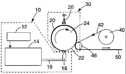
Referring now to Figure 1, adhesive coating station 10 includes adhesive
supply
12 which delivers adhesive to coating device 14. Coating device 14 delivers
adhesive
through line 16 to coating die 18. Thin adhesive layer 20 is applied onto
repeatably
reusable transfer surface 22 of rotating drum 24 by coating die 18. Rotating
drum 24 is
enclosed within electron beam apparatus 30. Electron beam source 26, enclosed
within
electron beam apparatus 30, supplies accelerated electrons to irradiate
adhesive layer 20
to chemically modify adhesive layer 20. Substrate supply roll 40 unwinds as
substrate
42 moves toward nip roller 46. Adhesive layer 20 contacts substrate 42 in a
nip formed
between nip roller 46 and rotating drum 24, after adhesive layer 20 is exposed
to
electron beam radiation. Irradiated adhesive layer 20 is transferred from
rotating drum
24 to substrate 42. Substrate 42 then carries adhesive layer 20 away from the
nip point,
resulting in adhesive coated web 50, which can be slit into tape.
Adhesive can be continuously coated upon repeatably reusable transfer surface
22 of rotating drum 24 and continuously transferred to substrate 42 when a
continuous
manufacturing process is desired. Alternatively, intermittent adhesive coating
may be
used in an otherwise continuous system to eventually produce adhesive patches
of
desired size on substrate 42.
Referring now to Figure 2, adhesive coating die 118 applies a layer of
adhesive
120 onto release surface 104 which is depicted as a belt moving between nip
roller 106
and roller 108. Adhesive 120 is then applied to repeatably reusable transfer
surface 122
of rotating drum 124 in a nip formed between nip roller 106 and rotating drum
124 to
move the adhesive through electron beam apparatus 130 which includes electron
beam
-4-
CA 02381883 2002-02-13
WO 01/15820 PCT/US00/19651
source 126 that irradiates the adhesive layer to chemically modify adhesive
layer 120.
Substrate supply roll 140 unwinds as substrate 142 moves toward nip roller
146.
Adhesive layer 120 contacts substrate 142 in a nip formed between nip roller
146 and
rotating drum 124, after adhesive layer 120 is exposed to electron beam
radiation.
Irradiated adhesive layer 120 is thereby transferred from repeatably reusable
transfer
surface 122 of rotating drum 124 to substrate 142. Substrate 142 then carries
adhesive
layer 120 away from the nip point, resulting in adhesive coated web 150, which
can be
slit into tape.
Adhesive can be continuously coated upon release surface 104 and continuously
transferred to substrate 142 when a continuous manufacturing process is
desired.
Alternatively, intermittent adhesive coating may be used in an otherwise
continuous
system to produce adhesive patches of desired size on substrate 142.
Satisfactory transfer from the release surface to the transfer surface is
achieved
when any residual of the adhesive material that may be left on the release
surface is
insufficient to result in an unsatisfactory coating quality or thickness
variation in the
adhesive that moves to the transfer surface. Factors that affect satisfactory
transfer
include the temperature of the release surface, temperature of the transfer
surface,
adhesive temperature, temperature of the rollers, line speed, adhesive
composition,
percent contact area between the adhesive and transfer surface, etc. These
operating
parameters should be selected to obtain correct rheology of the adhesive
composition
for the intended operation.
The electron beam modifiable adhesive layer may be coated into a layer of
desired thickness by various coating methods including solvent casting, latex
casting,
calendering, extrusion coating or hot melt coating. The coating may be applied
directly
to a repeatably reusable transfer surface, as shown in Figure 1.
Alternatively, the
coating may be applied to a release surface for subsequent application to a
repeatably
reusable transfer surface as illustrated by Figure 2. Drying or modifying the
temperature
of the electron beam modifiable adhesive layer can change its cohesive
strength and tack
and therefore enhance the ease of subsequent transfer step(s). Useful drying
techniques
are known in the art and determined by the method used to apply the adhesive
to the
release surface or transfer surface as well as the initial adhesive
composition.
-5-
CA 02381883 2002-02-13
WO 01/15820 PCTIUSOO/19651
Temperature modification can be done by techniques known in the art, including
exposure to ambient, blown, or cooled gas, infrared heaters, and contact with
a
temperature controlled roll.
An adhesive may also be applied first to a release surface and then
transferred to
a repeatably reusable transfer surface. The release surface may be a surface
of a drum or
a continuous belt. The release surface and the process conditions are selected
so the
electron beam modifiable adhesive layer, when in contact with both the release
surface
and the repeatably reusable transfer surface, preferentially adheres to the
transfer surface
under the chosen process conditions. The release surface can comprise such low
surface
energy materials as silicones, fluorinated polymers, long chain urethane or
acrylic
polymers.
The repeatably reusable transfer surface receives the electron beam modifiable
adhesive layer from either a release surface or from a coating device,
transports the
adhesive layer to an irradiation zone of an electron beam apparatus where the
adhesive is
exposed to electron beam radiation, and then transports the electron beam
modified
adhesive layer to a location where the electron beam modified adhesive layer
is
transferred to a substrate. The repeatably reusable transfer surface is
selected from the
group consisting of an ordered structured surface, a random structured
surface, and a
smooth surface. It may also include a temperature controllable surface. While
Figures 1
and 2 include the repeatably reusable transfer surface on a rotating drum, the
transfer
surface may be an elongated band or belt.
A smooth transfer surface contacts the adhesive over substantially all of its
surface extent and may have surface structure or pattern features of a depth
no greater
than 1 m. Such a transfer surface may adhere readily to an electron beam
modifiable
adhesive layer. The adhesive is coated upon the smooth transfer surface or is
transferred
from a release surface to the transfer surface. Then the adhesive is
irradiated before
transferring the adhesive to the substrate. However, adhesives generally
adhere both to
the materials useful as transfer surfaces as well as to the materials useful
as substrates,
making the subsequent transfer operation difficult. This problem can be solved
by
changing the adherence of the adhesive to the transfer surface by either
controlling the
-6-
CA 02381883 2002-02-13
WO 01/15820 PCT/US00/19651
contact area between the adhesive and the transfer surface or modifying the
temperature
of the transfer surface, or a combination thereof.
One preferred transfer surface comprises a repeating structured or patterned
surface effective to reduce surface contact between the transfer surface and
the
adhesive. The pattern may be raised above the general surface level of the
repeatably
reusable transfer surface or recessed into it, and it may be open or closed.
Open patterns allow air to bleed out from between the adhesive layer and the
patterned transfer surface. Examples of open patterns are parallel rows of
lines
separated by "V" shaped groves, where the lines are usually at various angles
relative to
each other, rows of recessed pyramids, and rows of cylindrical polygons.
Closed patterns generally trap air between the adhesive layer and the
patterned
transfer surface so air cannot bleed out from under the adhesive. Examples of
closed
patterns are polygons recessed beneath the transfer surface separated by lands
on the
transfer surface. The lands may be continuous or discontinuous. Figure 3 shows
a
triangular pattern recessed beneath the general surface level of the
repeatably reusable
transfer surface. Lands 32 form a triangular pattern on the transfer surface
that supports
the adhesive and separates the recessed polygons. Center to center distances
a, b, and c
define the dimensions between the center of each recessed polygon and the next
adjacent
recessed polygon. The center to center distances between two or more adjacent
recesses may be the same or different. Figure 4 shows a cube corner pattern
recessed
beneath the general surface level of the repeatably reusable transfer surface.
Lands 44
form a square pattern on the transfer surface. Center to center distances d
and e are
equal for the square pattern illustrated. Figure 5 illustrates a recessed
hexagon pattern
with lands 52 and center to center distances f and g.
Air bleed patterns may include a combination of both closed and open patterns,
for example a closed pattern wire screen over an open pattern such as a sand
blasted
surface or a parallel grooved surface. The pattern recesses can be very deep,
relative to
the adhesive thickness, because the adhesive is preferably supported by the
land surface
and contact with the depths of the pattern features can make transfer to the
substrate
more difficult.
-7-
CA 02381883 2002-02-13
WO 01/15820 PCT/US00/19651
Adhesive surface area of contact with the transfer surface varies with process
conditions and adhesive compositions, preferably from about 10 to 80% of the
adhesive
surface area. Higher surface contact levels are possible with lower tack
adhesives, and
process temperatures placing the adhesive rheology in a lower tack region.
Satisfactory
transfer of an adhesive layer from a release surface to a patterned transfer
surface occurs
at room temperature with preferably at least 10% (more preferably 20%) of the
adhesive
surface area in contact with the patterned transfer surface. Satisfactory
transfer of the
adhesive to a substrate from the transfer surface occurs at room temperature
if there is
preferably less than about 80% (more preferably less than about 60%) of the
adhesive
surface area in contact with the patterned transfer surface. A preferred
ordered transfer
surface comprises a layer having a multiplicity of structured recesses with
structure
depths sufficient to prevent the unmodified adhesive from wetting a sufficient
area of the
recess to adversely hinder subsequent transfer to a substrate (e.g., substrate
42). The
preferred structured recesses have structure center to center distances (i.e.,
the distance
from the center of one recess to the center of the next adjacent recess)
sufficiently close
to support the adhesive on the transfer surface and to prevent excessive sag
of the
adhesive layer into the pattern recesses. Excessive sag reduces the contact
area between
an irradiated adhesive and a substrate, inhibiting effective transfer. More
specifically,
the preferred depth of the recesses ranges from about 1 to 2000 m (more
preferably
100 to 1000 m) and the structure center to center distances between about 50
and
6000 m (more preferably 200 to 2000 m). Thus, structured transfer surfaces
range
from virtually smooth to macroscopic patterns. Structured surfaces can be made
by any
method known in the art including, for example, electroforming, embossing,
etching,
machining, molding, or sandblasting.
The preferred degree of contact changes with the adhesive composition. If the
adhesive sags or flows into the pattern recesses, satisfactory transfer of the
adhesive
layer to the substrate surface may be detrimentally affected. Sagging is
influenced by the
stiffness of the adhesive, the width of the recesses of the pattern, and the
width of the
land areas between the recesses of the pattern. Reducing the temperature or
changing
the composition can increase the adhesive stiffness. Generally, the width of
the recesses
in the pattern at room temperature should be less than about 2.0 millimeters
(mm),
-8-
CA 02381883 2002-02-13
WO 01/15820 PCT/US00/19651
preferably less than 1.5 mm, and most preferably less than 0.6 mm. For
example, if the
pattern were a screen, the mesh openings should be less than about 2.0 mm,
preferably
less than 1.5 mm, and most preferably less than 0.6 mm.
In addition, a pattern with sufficiently wide land area for surface contact
can
behave as a smooth transfer surface. Such a pattern could retain residue from
the
adhesive after the transfer of the adhesive to the substrate surface, or even
prevent
transfer. At room temperature, the greatest width of the pattern lands for
adhesive
surface area contact should generally be less than 240 m, preferably less
than 130 m,
and more preferably less than 76 m. A pattern with wide land areas for
surface contact
may also be treated as a smooth surface as noted above.
Another preferred transfer surface is a smooth surface that is either heated
or
cooled to achieve required tackiness of the adhesive when coating upon or
transferring
from the release surface to the transfer surface and from the transfer surface
to the
substrate. A temperature controllable surface allows various options in
heating and
cooling the transfer surface to match the adhesive properties at various
temperatures in
order to facilitate application of the adhesive to the transfer surface and
then to the
substrate. One option is cooling hot adhesive after applying the adhesive to
the transfer
surface with additional cooling after electron beam exposure, so the transfer
surface may
be relatively cool when the adhesive is applied to the substrate. Another
option is
heating the adhesive to a lower tack level at the transfer surface to
preferentially adhere
the adhesive layer to a relatively cool substrate and permit satisfactory
transfer to the
substrate surface. Thus, the process conditions are adapted for the rheology
of the
adhesive composition. Examples of means for obtaining controlled differences
in
temperatures between the two surfaces of the adhesive layer include: heated or
cooled
nip rolls; infrared lamps; and heated or cooled gas blowers.
Adhesive may fill in the structures in the repeatably reusable transfer
surface
when applying adhesive directly to that surface. Casting an adhesive film then
dropping
this film onto the surface, using a temperature controllable transfer surface,
using a
smooth transfer surface, or combinations thereof are therefore preferred for
the direct
adhesive application methods.
-9-
CA 02381883 2002-02-13
WO 01/15820 PCT/US00/19651
The transfer surface may be designed to permit variable pressure to contact
the
adhesive layer. A reduced pressure can help transfer adhesive from the release
surface
to the transfer surface. Reduced pressure could be generated, for example, by
creating a
partial vacuum behind a perforated transfer surface in a region where adhesive
on the
release surface contacts the transfer surface. Increased pressure can force
the adhesive
from one surface onto another surface. An increased pressure could be
generated, for
example, by creating a higher pressure region behind a perforated transfer
surface where
the adhesive contacts the substrate and is transferred thereto. This is more
desirable
when low adhesion substrate surfaces are used. Such substrates include release
liners
useful in transfer tape constructions, open weave fabrics, and loose nonwoven
webs.
The transfer surface may be a continuous belt or drum or may be a sleeve that
is
placed on or around a continuous belt or drum. The repeatably reusable
transfer surface
is resistant to degradation under electron beam irradiation so it may be
exposed to the
electron beam preferably at least 5 times (more preferably 50 times). Suitable
materials,
which are known to be resistant to electron beam degradation, include ceramics
and
metals, such as stainless steel, chrome, copper, nickel, brass, and aluminum.
The adhesive typically comprises one or more electron beam modifiable
elastomers and optionally one or more tackifying resins. The electron beam
modifiable
adhesive layer is selected from the group consisting of acrylics, natural
rubbers,
polybutadienes, polyisoprenes, styrene/butadiene copolymers, styrene/isoprene
copolymers, and silicones. The adhesive may also contain one or more additives
such as
antioxidants, crosslinking agents, fillers, pigments, plasticizers, and UV
stabilizers. The
adhesive may be pressure sensitive, having a composition that is tacky at the
use
temperature and that adheres with finger pressure. The thickness of the
adhesive layer
useful in the present invention covers the range commonly used in the industry
and is
generally between about 15 m and 1000 m.
An electron beam apparatus includes an electron beam source that directs
electrons into an electron beam modifiable material. The electron beam
apparatus
provides a typical dose of 5 to 100 kiloGray (kGy) (0.5 to 10.0 MRad) with
electrons
under an accelerating potential of 30 to 300 kiloVolts (kV). The electron beam
source
may be any electron beam source that emits electron beam radiation sufficient
to achieve
-10-
CA 02381883 2002-02-13
WO 01/15820 PCT/US00/19651
a desired degree of modification in an electron beam modifiable adhesive
layer. The
electrons travel from the electron beam source, which is maintained in a
vacuum,
through an electron beam window into an air gap between the window and the
adhesive
to be irradiated. The air gap is usually maintained at about atmospheric
pressure. The
exposure frequently occurs in an inert atmosphere but can occur in air or in a
vacuum
depending on the composition of the electron beam modifiable adhesive used.
Then the
electrons travel through the adhesive toward a metal surface, such as the
repeatably
reusable transfer surface. Manufacturers of suitable electron beam radiation
sources
include Energy Sciences Inc., in Wilmington, Massachusetts, and RPC
Industries, in
Hayward, California.
Radiation exposure can be varied over the cross-section of an adhesive layer
without degrading a substrate because radiation exposure occurs before the
adhesive
layer is applied to the substrate according to the present invention. When the
radiation
is applied after the adhesive has been coated on a substrate using the
conventional
process, the dose received by a typical adhesive layer thickness of 38.1 m
(1.5 mil) and
the dose received by a typical paper substrate for various accelerating
potentials is
shown in Figure 6. At an accelerating potential of 125 kV, the dose received
by a front
surface of the adhesive layer is greater than that received by a back surface
of the
adhesive that is adjacent to the substrate. At 200 kV, the dose is
substantially the same
throughout the adhesive layer thickness. At 300 kV, the dose is lower at the
front
surface of the adhesive than at the back surface. For all three profiles, the
adhesive is
irradiated while it is in contact with (i.e., immediately adjacent or
touching) the substrate
with the adhesive layer between the electron beam source and the substrate. At
least
some irradiation passes through the adhesive and into the substrate. In
contrast, the
inventive process electron beam modified adhesive layer is subsequently
transferred to a
substrate, reversing the dose profile of the conventional process so that the
adhesive
surface nearest the electron beam source becomes the interface between the
adhesive
and the substrate.
In order to achieve a sufficient electron beam dose to crosslink an adhesive
layer
at an interface with a substrate by a conventional process, some penetration
by electrons
into the substrate necessarily occurs. This penetration may cause electron
beam
-11-
CA 02381883 2002-02-13
WO 01/15820 PCT/US00/19651
modification of the substrate. A typical energy deposition profile or depth-
dose curve
(i.e., the energy absorbed by each material in the electron beam path) usually
reaches a
peak in the window and air gap regions or in the adhesive or substrate
regions. A
square-wave energy deposition curve, such that the adhesive layer receives a
similar
dose throughout its thickness while the substrate receives no energy, is not
physically
possible. Thus, when irradiating adhesive on a substrate in a known process,
the
substrate is exposed to electron beam radiation that may graft the adhesive to
the
substrate, but the radiation may also cause degradation in the substrate, such
as
indicated by a reduction in mechanical flexibility. If a liner is used as a
carrier material
for the adhesive instead of the intended substrate, then removal of the
adhesive from the
liner is affected by adhesion between the adhesive and the release surface as
a result of
irradiation that can graft the materials together. This also results in an
extra
manufacturing step and wasted material when the carrier material is discarded.
The present invention avoids these problems and offers further process
advantages. By controlling the dose and accelerating voltage, the electron
beam
modified adhesive layer may have an electron beam modification profile
selected from
the group consisting of an increasing degree of crosslinking through the
adhesive
thickness from a surface toward the substrate, a substantially uniform degree
of
crosslinking through the adhesive thickness, a decreasing degree of
crosslinking through
the adhesive thickness, and a peak level of crosslinking within the adhesive
between the
surface and the substrate. These profiles can be accomplished while the
resulting
construction of adhesive and substrate has a mechanical flexibility that is
not
substantially different from the flexibility of a construction having no
electron beam
modification, as measured by the number of bending cycles to break the
construction
using the MIT Folding Endurance Test described below.
Reflection of electrons off a metal surface, called backscatter, increases
with the
accelerating voltage and with increasing atomic number of the metal in the
surface.
Backscatter can be used advantageously to control the depth/dose gradient, and
to
achieve a peak level of crosslinking within the adhesive thickness.
Further modification of the depth/dose curve through the adhesive may be
achieved by selecting an electron beam window of lower density and/or lower
thickness,
-12-
CA 02381883 2002-02-13
WO 01/15820 PCT/US00/19651
and by selecting a smaller air gap between the electron beam window and the
adhesive,
such that voltages of less than 100 kV may be used. These attributes reduce
the unit
path thickness of the electron beam operation. "Unit path thickness" means the
product
of thickness times the density for a given combination of materials in the
electron beam
path. The density and thickness of each material in the path of an accelerated
electron
can be converted to an equivalent cross-section. For example, if a 300 kV
electron can
adequately penetrate a material having a density of 1.0 gram per cubic
centimeter (g/cc)
and a thickness of 500 m, it can penetrate a material having a density of 0.5
g/cc and a
thickness of 1000 m or a material having a density of 2.0 g/cc and a
thickness of
250 m. Useful electron beam windows include aluminum, beryllium, boron
nitride,
silicon, silicon nitride, titanium, and polymeric films such as polyimide
films. When a
polymeric film is used, a protective layer is placed on at least one surface
of the film in
order to improve performance and durability. The protective layer may be a
thin layer of
aluminum or other metal that provides protection against free-radical
degradation and
enhances thermal and electrical conduction along the film.
The smaller unit path thickness of a thinner or lower density electron beam
window and narrower air gap of only a few millimeters allows the peak in the
depth-dose curve to be shifted into the thickness of the adhesive. This causes
the level
of crosslinking within the body of the adhesive to be higher than either the
crosslinking
level at the front or rear surface.
The substrate may be any common paper or film presently known in the art.
Examples of such substrates include, for example, metal foils, metal coated
polymeric
films, polymeric films, paper, creped paper, cloth or non-wovens, and release
coated
papers and films. However, greater advantages are achieved with the present
invention
when the selected substrate is radiation degradable because the substrate is
not
irradiated by an electron beam with the present invention. A preferred
radiation
degradable substrate is selected from the group consisting of cellulose-based
non-woven
fabrics, cellulose-based woven fabrics, paper, polyisobutylene films,
polypropylene films,
polypropylene-based nonwovens, polytetrafluoroethylene films, vinyl films, and
combinations thereof. The substrate surface is preferably in web form.
-13-
CA 02381883 2002-02-13
WO 01/15820 PCT/US00/19651
One embodiment of the present invention is an adhesive coated web in which the
substrate has no electron beam radiation modification and no electron beam
radiation
degradation, both as described hereinabove. The adhesive also contains no
substantial
quantity of chemical, thermal, or ultraviolet crosslinking agent and is
preferably pressure
sensitive. The adhesive can be attached to the substrate, and in contact with
(i.e.,
immediately adjacent or touching) a radiation degradable component of the
substrate, so
that the bond between the adhesive and the substrate is stronger than a
subsequent bond
between the adhesive coated web and a work piece. The adhesive preferably has
a
cohesive strength greater than the strength of the subsequent bond.
Preferably, the
adhesive is permanently attached to the substrate.
Alternatively, the adhesive can be separably attached to the substrate so that
the
bond between the adhesive and the substrate is weaker than a subsequent bond
between
the adhesive coated web and a work piece. This can be achieved by including a
release
coating on one or both major surfaces of the substrate. A substrate having a
functionally
different release level on each major surface allows the surface of the
substrate with a
higher release level to preferentially adhere to the adhesive, to remove the
adhesive from
the transfer surface. Then, this differential release substrate may be rolled
upon itself.
This results in an adhesive transfer tape that allows the adhesive to be
transferred to a
workpiece by adhering the tape construction to the workpiece and then removing
the
differential release substrate, leaving only the adhesive on the workpiece.
The exposed
surface of the transferred adhesive is then available to bond the workpiece to
another
object. Typical release coatings graft to electron beam modified adhesives
during the
irradiation process making adhesive transfer tapes with electron beam modified
adhesives unknown to the art. However, with techniques such as the temperature
and
pressure assisted transfer described herein, such tape constructions are now
possible.
The adhesive can have a patterned surface (i.e., a network of lines on the
surface
in a visible pattern). Such a pattern may closely or roughly replicate any
pattern found
on the repeatably reusable transfer surface.
This invention is useful for electron beam radiation crosslinking adhesives
that
are included in tape constructions having radiation degradable backings. The
inventive
method permits manufacturing constructions that take advantage of the electron
beam
-14-
CA 02381883 2002-02-13
WO 01/15820 PCT/US00/19651
process without the adverse substrate effects that are commonly associated
with
electron beam radiation. More specifically, this allows extrusion coating
adhesives
having relatively lower molecular weight, then building up the adhesive shear
strength
through electron beam radiation crosslinking. Inexpensive tape backings that
are
typically radiation degradable can then be used with no loss in flexibility.
Such a method
also permits the manufacture of a variety of electron beam modified adhesive
transfer
tapes.
Objects and advantages of this invention are further illustrated by the
following
examples, but the particular materials and amounts thereof recited in these
examples, as
well as other conditions and details, should not be construed to unduly limit
this
invention.
Percent Wetted Contact
The adhesive was laminated to a structured surface with a specific pattern and
the pattern/adhesive assembly was photographed under a microscope with
reflected light
to determine the percent contact area between the adhesive and the pattern.
The contact
area was distinctly white under magnification whereas all other areas were
translucent.
The percent area contact was calculated by dividing the contact area of one
region by
the total area of that region.
MIT Folding Endurance
A 125 mm wide strip was cut from an adhesive layer on a substrate. The strip
was clamped in a Flex Tester MIT Model #1 (from Tinius Olsen Testing Machine
Co.,
Willow Grove, Pennsylvania). The tester repeatedly bent the strip 270 until
the strip
broke. The number of cycles until break was recorded as a measure of the
practical
strength.
Adhesion to Substrate
Adhesive tape samples 1.25 centimeters (cm) wide and 15 cm long were tested
for adherence to the substrate. A strip was cut from the sample construction
to be
tested, placed together adhesive-to-adhesive with a strip of a second and
different
reference adhesive tape, in which the adhesion of the adhesive to substrate
was
necessarily stronger than the expected adhesion of the tested adhesive to its
substrate.
-15-
CA 02381883 2002-02-13
WO 01/15820 PCT/USOO/19651
The test samples and reference tapes were adhered to each other by rolling
them under
the pressure of four passes of a 2.1 kg (4.5 lb.) roller. After aging at
ambient tempera-
tures (about 22 C) for approximately one hour, the tapes were peeled apart
using a
Model 3M90 slip/peel tester (from Imass, Inc., Accord, Massachusetts) in 180
geometry at 230 cm/min. (90 in./min.) peel rate to determine the force needed
in N/dm
to separate the adhesive of the sample from its substrate.
Examples
Transfer Surfaces: Examples 1-11
In Example 1, an adhesive was prepared with 55 parts (by weight) Standard
Malaysian Rubber (SMR) CV 60 natural rubber (available from Lewis & Peat,
Middlebury, Connecticut), 55 parts aliphatic olefin tackifying resin
(EscorezTM 1304,
available from Exxon Chemical Co., Houston, Texas), 45 parts styrene-butadiene
random copolymer rubber (SynpolTM 1011A, available from Ameripol Synpol Corp.,
Akron, Ohio), and 1.1 parts antioxidant (IrganoxTM 1010, available from Ciba-
Geigy
Corp., Hawthorne, New York). The adhesive was die coated at a 38 m (1.5 mil)
thickness onto a silicone release liner. Another release liner was placed on
the exposed
adhesive and then the assembly was wound for later use.
The second release liner was removed from a sample of the adhesive. This
adhesive sample was then laminated onto a transfer surface having Pattern A,
shown in
Figure 3 with the dimensions included in Table 1. The lamination force was 45
N
(10 lb.), provided by a 38 mm (1.5 in.) diameter 50 mm (2 in.) wide rubber
roller. The
percent wetted contact (adhesive surface area contacting the pattern) was
determined
using an optical microscope.
The adhesive was transferred to a saturated paper masking tape substrate by
wrapping a 2.5 cm (1.0 in) x 11.9 cm (4.7 in) sheet of the 127 m (5 mil)
thick substrate
around the rubber roller, rolling the substrate wrapped roller over the
adhesive at
approximately 1.0 m/sec with approximately 45 N (10 lb.) force. A visual
determination
was made as to the reliability and completeness of transfer. The data is shown
in
Table 2.
-16-
CA 02381883 2002-02-13
WO 01/15820 PCT/US00/19651
The transferred adhesive of Example 2 was as in Example 1, except the adhesive
was laminated to the pattern with 178 N (40 lb.) force instead of a 45 N (10
lb.) force,
resulting in a different percent wetted contact than obtained in Example 1.
The percent
wetted contact was determined and a visual determination was made as to the
reliability
and completeness of transfer. The data is shown in Table 2.
The transferred adhesives of Examples 3-11 were as the Examples 1-2, except
different patterns, resulting in different percent wetted contact were used.
The
transferred adhesives of Examples 10-11 were like Example 1, except a smooth
pattern,
resulting in essentially complete wetted contact, was used and the lamination
was done
at room temperature for Example 10 and 120 C for Example 11. The pattern type,
lamination force, wetted contact percent, and visual assessments of the
transfer of the
adhesive layer to the substrate are listed in Table 2. Patterns A and D are
shown in
Figure 3. Patterns B and C are shown in Figure 4. Pattern E is shown in Figure
5.
Table 1: Surface Contact for Various Patterns
Pattern Ex. Pattern Shape Surface Pattern Pattern
Type Contact Dimensions: Dimensions:
Width Base Depth
m (mil) m (mil) m (mil)
A 1,2 Recessed Triangle 40.6, 81.3 1680, 1720, 1958 711 (28)
1.6, 3.2 (66.1, 67.7, 77.1
B 3,4 Recessed Cube 66.0 (2.6) 866, 866 533 (21)
Corner (34.1, 34.1)
C 5,6 Recessed Cube 61.0 (2.4) 584, 584 356 (14)
Corner (23, 23)
D 7,8 Recessed Triangle 55.9, 25.4 411, 411, 467 178 (7.0)
(2.2, 1.0) (16.2, 16.6, 18.4)
E 9 Recessed Hexagon 240 (9.5) 2057 (81) 2057 (81)
F 10, 11 Smooth Flat surface Flat surface Flat surface
The adhesives in Examples 1-11 were not irradiated because it was determined
that irradiation was not necessary to evaluate the transfer viability of the
various
patterns.
-17-
CA 02381883 2002-02-13
WO 01/15820 PCTIUSOO/19651
Table 2: Transfer Quality Rating of Various Patterns
Ex. Pattern Lamination Temp. of Percent Transfer Quality Rating
Type Force Transfer Wetted
N(]b.) Surface Contact Release-to- Transfer
(oC) Transfer Surface-to-
Surface Substrate
1 A 44.5 (10) 22 11.5 Fair Good
2 178 (40) 14.2 Fair Good
3 B 44.5 (10) 22 14.8 Fair Good
4 178 (40) 17.3 Good to Fair Good
C 44.5 (10) 22 20.2 Good Good
6 178 (40) 22.5 Good Good
7 D 44.5 (10) 22 24 Good Good
8 178 (40) 22 35 Good Good to Fair
9 E 44.5 (10) 22 13.0 Fair Fair to Poor
F 44.5 (10) 22 100 Good Poor
(Smooth)
11 N/A 120 100 N/A Good
Good = Completely and cleanly transferred
Fair = Some incomplete or flawed transfer but acceptable
Poor = Failure to transfer at all
5 The hexagonal pattern in Example 9 had borders 240 m (9.5 mil) wide and a
relatively low surface contact of 13%. The transfer of the adhesive to the
substrate was
marginally satisfactory at room temperature because the adhesive sagged into
the
recessed pattern and did not contact the substrate enough to ensure good
transfer. Also,
the large supported contact area at the pattern borders did not transfer
readily due to the
10 essentially complete adhesive contact in that local area. This indicated
that the local
contact width and the spacing between contact areas was important even when
the total
percent wetted contact was at the lower end of the range.
Generally, the transfer from the release surface to the drum transfer surface
was
made easier by contact areas at the higher end of the range with a smooth drum
providing the easiest transfer. Transfer from the drum to the substrate was
made easier
by contact areas on the low end of the range, from about 10 to 20 percent
wetted
contact area. For the adhesion and release properties for the adhesive,
release liner, and
-18-
CA 02381883 2002-02-13
WO 01/15820 PCT/US00/19651
substrate used in this series of examples, the acceptable range of wetted
contact at room
temperature was between about 10 and 40 percent. The upper limit of the range
increases to about 80 to 100 percent wetted contact area when the transfer
surface was
heated. Thus many patterns were possible at room temperature, and the pattern
possibilities increased when the transfer surface temperature was controlled.
Substrate Degradation: Comparative Examples C1-C10, Examples 12-13
In Comparative Example C1, a rubber based adhesive was formulated with 55
parts (by weight) SMR CV 60 natural rubber, 50 parts aliphatic olefin
tackifying resin
(EscorezTM 1304), 45 parts styrene-butadiene random copolymer rubber (SynpolTM
1011A), 2.0 parts titanium dioxide, 1.0 parts antioxidant, 1.5 parts linear
low density
polyethylene (DowlexTM 6806, available from Dow Chemical Co., Midland,
Michigan),
and 1.5 parts styrene-isoprene-styrene (SIS) block copolymer (KratonTM 1107,
available
from Shell Chemical Co., Houston, Texas).
The adhesive was die coated with a die coater at a thickness of 58 m (2.3
mil)
onto a continuous silicone release belt (No. 2015 from Voss Belting of
Lincolnwood,
Illinois). The release belt passed over a temperature controlled driven backup
roller
maintained at 30 C at 15.2 m/min (50 feet per minute (fpm)). The adhesive
layer on the
silicone belt passed through an entrance slot into the lead lined chamber of
the electron
beam exposure unit (described above) while the electron beam source power was
off,
and placed in contact with a nickel transfer surface having Pattern B
(described in Table
1 and illustrated in Figure 4). This transfer surface was in the form of a
sleeve over a
driven drum with a diameter of 460 mm (about 17 in.) that was maintained at
room
temperature (about 22 C). Two successive nip rolls held the release belt
against the
drum transfer surface for more than twice the time and area provided by one of
the nip
rollers. The adhesive layer was pressed onto the transfer surface with 89 N
(20 lb.)
force by these nip rollers. The adhesive layer transferred cleanly to the
transfer surface
and then passed under the electron beam source which was turned off. A paper
masking
tape substrate was routed into the electron beam chamber through a slot on the
side of
the chamber after (or downstream of) the irradiation zone (i.e., the part of
the chamber
in which the electron beam radiation is directed toward a work piece or
substrate). The
-19-
CA 02381883 2002-02-13
WO 01/15820 PCTIUSOO/19651
adhesive layer was placed in contact with the surface of this substrate by two
successive
nip rolls behind the substrate. These two nip rolls increased the time of
adhesive contact
and the area of adhesive under pressure, when compared to a single nip roll.
The nip
rolls each pressed the adhesive layer onto the paper masking tape substrate
surface with
a force of 89 N (20 lb.).
The adhesive layer was transferred cleanly to the paper masking tape substrate
surface, wound up into a roll, and subsequently unwound and tested for backing
flexibility as per the MIT Folding Endurance Test, the average value of five
tests of
which are reported in Table 3.
The adhesive tape constructions of Comparative Examples C2-C 10 were made
as in Comparative Example C1, except that the resulting adhesive tape rolls
were then
passed straight through the electron beam exposure unit with the electron beam
source
power on. The drum transfer surface was bypassed, such that the adhesive layer
would
be irradiated while in contact with the paper masking tape substrate. The
electron beam
was adjusted to irradiate the top surface of the adhesive layers at various
accelerating
potentials with various doses as listed in Table 4. The webs were then rolled
up and
subsequently unwound and tested for backing flexibility as per the MIT Folding
Endurance Test, the average value of three tests of which are reported in
Table 3.
The adhesive tape constructions of Examples 12-13 were made as in
Comparative Example Cl, except that the electron beam exposure unit was on and
adjusted to irradiate the top surface of the adhesive layers at an
accelerating potential of
200 kV with various doses as listed in Table 3. The webs were then rolled up
and
subsequently unwound and tested for backing flexibility as per the MIT Folding
Endurance Test, the average value of three tests of which are reported in
Table 3.
-20-
CA 02381883 2002-02-13
WO 01/15820 PCT/US00/19651
Table 3: Folding Endurance
Example Potential Dose MIT Folding Endurance Percent Reduction in
kV kGy Average Cycles Folding Endurance
C1 0 0 730 Baseline
C2 125 40 746 -2 (increase)
C3 125 70 666 9
C4 125 100 619 15
C5 150 40 583 20
C6 150 70 425 42
C7 150 100 315 57
C8 200 40 449 38
C9 200 70 238 67
C10 200 100 131 82
12 200 40 791 -8 (increase)
13 200 100 792 -8 (increase)
Substrate degradation was determined by comparing the average number of
folding cycles of each of the examples relative to that samples with little or
no
irradiation. No substrate degradation was evident in Comparative Examples C
1(no
irradiation) or C2 (least severe irradiation). Comparative Examples C2-C 10
were
irradiated while the adhesive was on the substrate. Electron beam radiation
modification
and degradation of the Comparative Examples increased in proportion to the
exposure
levels. Substantial electron beam degradation occurred in Comparative Examples
C3
through C 10.
In contrast, no electron beam radiation modification and no electron beam
substrate degradation was evident in the inventive process (Examples 12-13) in
which
the adhesive layer was exposed to comparable irradiation conditions,
demonstrating the
advantage of this invention. Although the irradiation conditions were adjusted
to deliver
the listed dose to the top surfaces of the adhesive layers, Figure 6
illustrates that a
significant amount of electron beam radiation necessarily reaches the
substrate when the
adhesive is exposed while in contact with the substrate. Holding the maximum
-21-
CA 02381883 2002-02-13
WO 01/15820 PCT/US00/19651
irradiation levels to the least severe conditions limits the substrate
degradation in the
conventional process, but this also limits the level of crosslinking in the
adhesive and
limits where the maximum dose can occur within the adhesive layer without
significant
substrate degradation. The present invention allows virtually any level of
adhesive
crosslinking and a peak dose anywhere within the adhesive thickness with no
substrate
degradation.
Adhesion to Substrates: Comparative Examples C11-C13, Examples 14-17
The adhesive layer constructions of Comparative Examples C 11 and C 12 were
made as in Comparative Examples C8 and C 10, respectively. The adhesive layer
constructions of Examples 14 and 15 were made as in Examples 12 and 13,
respectively.
The adhesive layer constructions of Examples 16 and 17 were made as in
Examples 12
and 13, respectively, except that the irradiated adhesive layer was exposed to
an air
atmosphere before being transferred to the substrate. Comparative Example C13
was
made by coating the adhesive directly onto the paper masking tape substrate
with a
conventional hot melt die coater at 45.7 m (1.8 mil) thickness, passing the
coated
construction at 61 m/s (200 fpm) under the electron beam set at 200 kV to
irradiate the
surface of the adhesive in a nitrogen atmosphere with a dose of 40 kGy (4
MRad), and
winding the construction into a roll. The conditions are listed in Table 4.
The
constructions were evaluated for adhesion of the adhesive to the substrate.
The data is
shown in Table 4.
-22-
CA 02381883 2002-02-13
WO 01/15820 PCT/US00/19651
Table 4: Adhesion to Substrate
Example Dose Irradiated Adhesion to Substrate
kGy N/dm
C 11 40 On Substrate 60
C12 100 On Substrate 61
14 40 Before Transfer, Nitrogen 60
15 100 Before Transfer, Nitrogen 57
16 40 Before Transfer, Air 60
17 100 Before Transfer, Air 60
C13 40 On Substrate 58
There was no significant difference in the adhesion of the backing to the
adhesive
whether the adhesive was irradiated before or after lamination to the backing,
whether
the transfer was performed in a nitrogen or air atmosphere, or whether it was
made by a
conventional process. The exposure conditions tested included the high end of
useful
exposures, sufficient to show any differences.
Dose Gradients: Examples 18-20
The adhesive constructions in Examples 18-20 were prepared as in Example 12
using Pattern B except the adhesive thickness was 46 m (1.8 mil),
accelerating
potentials were chosen that gave varying dose gradients (and therefore
crosslink
gradients) through the adhesive. Radiachromic film dosimeters (FWT-60-00,
available
from Far West Technology, Inc., Goleta, California) were staggered on both
sides of the
adhesive to be irradiated (never one dosimeter directly above another) and
then removed
from the tape assembly and read after completion of the process. A Model 92
Radiachromic Reader (available from Far West Technology) was used to determine
the
dosage received by each dosimeter. The conditions and dosimeter readings are
shown in
Table 5. The top side of the adhesive layer is defined as the side exposed to
the
atmosphere and the bottom side is defined as the side adhered to the substrate
in the
final product.
-23-
CA 02381883 2002-02-13
WO 01/15820 PCT/US00/19651
Table 5: Dose Gradients
Example Adhesive Accelerating Relative Dose
Side Voltage (kV) (kGy)
18 Top 125 0.18
Bottom 125 1.00
19 Top 200 1.00
Bottom 200 1.00
20 Top 300 1.06
Bottom 300 1.00
The dosimeters were 43 m (1.7 mil) thick so the exact gradient through the
adhesive layer could not be measured using this technique, although a general
trend was
observed. This indicated a decreasing dose gradient through the adhesive layer
at an
accelerating potential of 125 kV, a uniform dose gradient through the adhesive
layer at
an accelerating potential of 200 kV, and an increasing dose gradient through
the
adhesive at an accelerating potential of 300 W. This was done without
irradiating the
backing, something not possible using conventional techniques.
Temperature, Pattern, Substrate: Examples 21-27
Adhesive constructions were made for Examples 21-27 as in Example 12, except
various drum temperatures (either maintained at 21 C (70 F) or heated to 49 C
(120 F)), transfer surface pattern shapes and depths (Patterns A, B, and C
described in
Table 1 and shown in Figures 3 and 4), substrate types (paper as in Example 12
or
100 m (4 mil) polyethyleneterephthalate film), and speeds between 6 and 40
m/min (20
and 130 fpm) were used as shown in Table 6. The unmodified adhesive layer of
each
example transferred cleanly from the release surface to the transfer surface
and the
irradiated adhesive layer of each example transferred cleanly from the
transfer surface to
the substrate.
-24-
CA 02381883 2002-02-13
WO 01/15820 PCTIUSOO/19651
Table 6: Temperature, Pattern, and Substrate
Example Drum Temperature Transfer Pattern Substrate Speed
C Shape m/min (fpm)
21 21 Pattern A paper 40 (130)
22 21 Pattern B paper 37 (120)
23 21 Pattern B film 6(20)
24 21 Pattern C paper 37 (120)
25 21 Pattern C film 18 (60)
26 49 Pattern B paper 37 (120)
27 49 Pattern C paper 37 (120)
These examples showed that controlling the transfer surface, having various
patterns, to ambient and higher temperatures allowed satisfactory transfer of
the
adhesive before and after irradiation.
Cooled Transfer Surface: Examples 28-29
The pressure-sensitive adhesive constructions of Examples 28-29 were
formulated with a composition of 95 weight percent isooctyl acrylate and 5
weight
percent acrylic acid that was water emulsion polymerized and had a shear
viscosity of
150 Pa-s and was dried. This composition was blended with 1.5 parts
polyethylene
(DowlexTM 6806, available from Dow Chemical Co., Midland, Michigan) and 1.5
parts
styrene-butadiene rubber (KratonTM 1107, available from Shell Chemical Co.,
Houston,
Texas).
The inventive process was run at 6 m/min. (20 fpm). The drum transfer surface
was cooled to 4 C (40 F) for Example 28 and maintained at 21 C (70 F) for
Example
29. The unmodified adhesive layer of each example transferred cleanly from the
release
surface and the irradiated adhesive layer of each example transferred cleanly
from the
transfer surface to the substrate. These examples showed that controlling the
transfer
surface to ambient and lower temperatures allowed satisfactory transfer before
and after
irradiation.
-25-
CA 02381883 2002-02-13
WO 01/15820 PCT/US00/19651
Screen Transfer Surfaces: Examples 30-37
A 50.8 m (2 mil) thick layer of the adhesive composition used in
Examples 12-13 (described above) was die coated onto a silicone release roll
and then
transferred to a screen belt that contacted the release roll at a nip point.
The belt
material was 50 x 50 bronze mesh screen (50 openings per horizontal linear
inch and 50
openings per vertical linear inch) (from McMaster-Carr Industrial Supply,
Chicago,
Illinois). The unmodified adhesive layer was carried by the belt through an
entrance slot
into the lead lined chamber of the electron beam exposure unit described above
and
irradiated using an accelerating potential of 175 kV to produce a surface dose
of 40 kGy
(4 MRad), and then passed from the chamber through an exit slot. The
irradiated
adhesive layer was placed in contact with the surface of a paper masking tape
substrate
by a nip roll behind the paper masking tape substrate and a nip roll beneath
the belt such
that the irradiated adhesive layer was pressed onto the paper masking tape
substrate
surface with sufficient force to transfer the irradiated adhesive layer to the
substrate.
The adhesive layer was transferred cleanly to the paper masking tape substrate
surface
and wound up into a roll.
Other screen configurations (also available from McMaster-Carr) were also
tested and the resulting transfer ratings appear in Table 7.
Table 7: Screen Transfer Surfaces
Example Screen Mesh Size and Material Transfer Quality Rating
14 x 14 Brass Poor
31 30 x 30 Galvanized Steel Fair
32 40 x 40 Aluminum Fair to Good
33 50 x 50 Brass Good
34 60 x 60 Stainless Steel Poor
100 x 100 Brass Good
36 100 x 100 Stainless Steel Good
37 200 x 200 Stainless Steel Fair to Good
-26-
CA 02381883 2002-02-13
WO 01/15820 PCT/US00/19651
These examples showed that both the screen mesh size and the screen material
were important. While several screen configurations can be used as transfer
surfaces,
the 50 x 50 brass was preferred for this adhesive composition and thickness.
Various modifications and alterations of this invention will become apparent
to
those skilled in the art without departing from the scope and principles of
this invention,
and it should be understood that this invention is not to be unduly limited to
the
illustrative embodiments set forth hereinabove.
-27-