Note: Descriptions are shown in the official language in which they were submitted.
CA 02381999 2002-02-13
WO 01/17122 PCT/CAOO/00996
-1-
Improved Method and Apparatus for Up- and Down- Conversion of Radio
Frequency (RF) Signals
The present invention relates generally to communications, and more
specifically, to a fully-integrable method and apparatus for up- and down-
conversion
of radio frequency (RF) and baseband signals with improved performance.
Background of the Invention
Many communication systems modulate electromagnetic signals from
baseband to higher frequencies for transmission, and subsequently demodulate
those high frequencies back to their original frequency band when they reach
the
receiver. The original (or baseband) signal, may be, for example: data, voice
or
video. These baseband signals may be produced by transducers such as
microphones or video cameras, be computer generated, or transferred from an
electronic storage device. In general, the high transmission frequencies
provide
longer range and higher capacity channels than baseband signals, and because
high
frequency RF signals can propagate through the air, they can be used for
wireless
channels as well as hard wired or fibre channels.
All of these signals are generally referred to as radio frequency (RF)
signals,
which are electromagnetic signals, that is, waveforms with electrical and
magnetic
properties within the electromagnetic spectrum normally associated with radio
wave
propagation. The electromagnetic spectrum was traditionally divided into 26
alphabetically designated bands, however, the International Telecommunication
Union (ITU) formally recognizes 12 bands, from 30 Hz to 3000 GHz. New bands,
from 3 THz to 3000 THz, are under active consideration for recognition.
Wired communication systems which employ such modulation and
demodulation techniques include computer communication systems such as local
area networks (LANs), point to point signalling, and wide area networks (WANs)
such as the Internet. These networks generally communication data signals over
electrical or optical fibre channels. Wireless communication systems which may
employ modulation and demodulation include those for public broadcasting such
as
AM and FM radio, and UHF and VHF television. Private communication systems
may include cellular telephone networks, personal paging devices, HF radio
systems
used by taxi services, microwave backbone networks, interconnected appliances
under the Bluetooth standard, and satellite communications. Other wired and
SUBSTITUTE SHEET (RULE 26)
CA 02381999 2002-02-13
WO 01/17122 PCT/CAOO/00996
-2-
wireless systems which use RF modulation and demodulation would be known to
those skilled in the art.
One of the current problems in the art, is to develop physically small and
inexpensive modulation and demodulation techniques and devices that have good
performance characteristics. For cellular telephones, for example, it is
desirable to
have transmitters and receivers (which may be referred to in combination as a
transceiver) which can be fully integrated onto integrated circuits (ICs).
Several attempts at completely integrated transceiver designs have met with
limited success. For example, most RF topology typically requires at least two
high
quality filters that cannot be economically integrated within any modern IC
technology. Other RF receiver topologies exist, such as image rejection
architectures, which can be completely integrated on a chip, but lack in
overall
performance. Most receivers use the "super-heterodyne" topology, which
provides
excellent performance, but does not meet the desired level of integration for
modern
wireless systems.
Existing transceiver solutions and their associated problems and limitations
are summarized below.
1. Super-heterodyne:
The super-heterodyne receiver uses a two-step frequency translation method
to convert an RF signal to a baseband signal. Figure 1 presents a block
diagram of
a typical super-heterodyne receiver 10. Generally, the mixers labelled Ml 12,
MI 14,
and MQ 16 are used to translate an incoming RF signal to baseband or to some
intermediate frequency (IF). The balance of the components amplify the signal
being processed and filter noise from it.
More specifically, the RF band pass filter (BPF1) 18 first filters the
incoming
signal and corruptive noise coming from the antenna 20, attenuating out of
band
signals and passing the desired signal (note that this band pass filter 18 may
also be
a duplexer). A low noise amplifier 22 then amplifies the filtered antenna
signal,
increasing the strength of the RF signal and reducing the noise figure of the
receiver
10. The signal is next filtered by another band pass filter (BPF2) 24 usually
identified
as an image rejection filter. The desired signal, plus residual unwanted
signals, then
enter mixer Ml 12 which multiplies this signal with a periodic sinusoidal
signal
generated by the local oscillator (LO1) 26. The mixer Ml 12 receives the
signal from
the image rejection filter 24 and causes both a down-conversion and an up-
SUBSTITUTE SHEET (RULE 26)
CA 02381999 2002-02-13
WO 01/17122 PCT/CAOO/00996
-3-
conversion in the frequency domain. Usually, the down-converted portion is
retained
at the so-called "Intermediate Frequency" (IF).
Generally, a mixer is a circuit or device that accepts as its input two
different
frequencies and presents at its output:
(a) a signal equal in frequency to the sum of the frequencies of the input
signals;
(b) a signal equal in frequency to the difference between the frequencies of
the
input signals; and
(c) the original input frequencies.
Note that the frequency conversion process causes a second band of
frequencies to be superimposed upon the desired signal at the IF frequency.
These
"image frequencies" are also passed by the band pass filter 24 and corrupt the
desired signal. Note also that the typical embodiment of a mixer is a digital
switch,
which may generate significantly more tones than those described in (a)
through (c).
The IF signal is next filtered by a band pass filter (BPF3) 28 typically
called
the channel filter, which is centred around the IF frequency, thus filtering
out mixer
signals (a) and (c) above.
The signal is then amplified by an amplifier (IFA) 30, and is split into its
in-
phase (I) and quadrature (Q) components, using mixers MI 14 and MQ 16, and
orthogonal mixing signals generated by local oscillator (L02) 32 and 90 degree
phase shifter 34. L02 32 generates a regular, periodic signal which is
typically tuned
to the IF frequency, so that the signals coming from the outputs of MI 14 and
MQ 16
are now at baseband, that is, the frequency at which they were originally
generated.
The two signals are next filtered using low pass filters LPFI 36 and LPFQ 38
to
remove the unwanted products of the mixing process, producing baseband I and Q
signals. The signals may then be amplified by gain-controlled amplifiers AGCI
40
and AGCQ 42, and digitized via analog to digital converters ADI 44 and ADQ 46
if
required by the receiver.
The main problems with the super-heterodyne design are:
= it requires expensive off-chip components, particularly band pass filters
18,
24, 28, and low pass filters 36, 38 to remove unwanted signal components;
= the off-chip components require design trade-offs that increase power
consumption and reduce system gain;
= image rejection is limited by the off-chip components, not by the target
integration technology;
= isolation from digital noise can be a problem; and
SUBSTITUTE SHEET (RULE 26)
CA 02381999 2002-02-13
WO 01/17122 PCT/CAOO/00996
-4-
it is not fully integratable.
2. Image Rejection Architectures:
Several image rejection architectures exist, but are not widely used. The two
most well known being the Hartley Image Rejection Architecture and the Weaver
Image Rejection Architecture. There are other designs, which are generally
based
on these two architectures, and other methods which employ poly-phase filters
to
cancel image components. Generally, either accurate signal phase shifts or
accurate generation of quadrature local oscillators are employed in these
architectures to cancel the image frequencies. The amount of image
cancellation is
directly dependent upon the degree of accuracy in producing the phase shift or
in
producing the quadrature local oscillator signals.
Although the integratability of these architectures is high, their performance
is
relatively poor due to the required accuracy of the phase shifts and
quadrature
oscillators. This architecture has been used for dual mode receivers on a
single
chip.
3. Direct Conversion:
Direct conversion architectures demodulate RF signals to baseband in a
single step, by mixing the RF signal with a local oscillator signal at the
carrier
frequency of the RF signal. There is therefore no image frequency, and no
image
components to corrupt the signal. Direct conversion receivers offer a high
level of
integratability, but also have several important problems. Hence, direct
conversion
receivers have thus far proved useful only for signalling formats that do not
place
appreciable signal energy near DC after conversion to baseband.
A typical direct conversion receiver is shown in Figure 2. The RF band pass
filter (BPF1) 18 first filters the signal coming from the antenna 20 (this
band pass
filter 18 may also be a duplexer). A low noise amplifier 22 is then used to
amplify the
filtered antenna signal, increasing the strength of the RF signal and reducing
the
noise figure of the receiver 10.
The signal is then split into its quadrature components and demodulated in a
single stage using mixers MI 14 and MQ 16, and orthogonal signals generated by
local oscillator (L02) 32 and 90 degree phase shifter 34. L02 32 generates a
regular, periodic signal which is tuned to the incoming wanted frequency
rather than
an IF frequency as in the case of the super-heterodyne receiver. The signals
coming from the outputs of MI 14 and MQ 16 are now at baseband, that is, the
frequency at which they were originally generated. The two signals are next
filtered
SUBSTITUTE SHEET (RULE 26)
CA 02381999 2002-02-13
WO 01/17122 PCT/CAOO/00996
-5-
using low pass filters LPFI 36 and LPFQ 38, are amplified by gain-controlled
amplifiers AGCI 40 and AGCQ 42, and are digitized via analog to digital
converters
ADI 44 and ADQ 46.
Direct conversion RF receivers have several advantages over super-
heterodyne systems in term of cost, power, and level of integration, however,
there
are also several serious problems with direct conversion. These problems
include:
= noise near baseband (that is, 1/f noise) which corrupts the desired signal;
= local oscillator (LO) leakage in the RF path that creates DC offsets. As the
LO frequency is the same as the incoming signal being demodulated, any
leakage of the LO signal onto the antenna side of the mixer will pass through
to the output side as well;
= local oscillator leakage into the RF path that causes desensitization.
Desensitation is the reduction of desired signal gain as a result of receiver
reaction to an undesired signal. The gain reduction is generally due to
overload of some portion of the receiver, such as the AGC circuitry, resulting
in suppression of the desired signal because the receiver will no longer
respond linearly to incremental changes in input voltage.
= noise inherent to mixed-signal integrated circuits corrupts the desired
signal;
= large on-chip capacitors are required to remove unwanted noise and signal
energy near DC, which makes integrability expensive. These capacitors are
typically placed between the mixers and the low pass filters; and
= errors are generated in the quadrature signals due to inaccuracies in the 90
degree phase shifter.
4. Near Zero-IF Conversion:
This receiver architecture is similar to the direct conversion architecture,
in
that the RF input signal band is translated brought close to baseband in a
single step
using a regular, periodic oscillator signal. However, the desired signal is
not brought
exactly to baseband and therefore DC offsets and 1/f noise do not contaminate
the
output signal. Image frequencies are again a problem though, as in the case of
the
super-heterodyne structure.
Additional problems encountered with near zero-IF architectures include:
= the need for very accurate quadrature local oscillators;
= the need for several balanced signal paths for purposes of image
cancellation;
SUBSTITUTE SHEET (RULE 26)
CA 02381999 2002-02-13
WO 01/17122 PCT/CAOO/00996
-6-
= noise inherent to mixed-signal integrated circuits which corrupts the
desired
output signal; and
= isolation from digital noise can be a problem.
5. Sub-sampling Down-conversion:
This method of signal down-conversion utilizes subsampling of the input
signal to effect the frequency translation, that is, the input signal is
sampled at a
lower rate than the signal frequency. This may be done, for example, by use of
a
sample and hold circuit.
Although the level of integration possible with this technique is the highest
among those discussed thus far, the subsampling down-conversion method suffers
from two major drawbacks:
= subsampling of the RF signal causes aliasing of unwanted noise power to
DC. Sampling by a factor of m increases the down-converted noise power of
the sampling circuit by a factor of 2m; and
= subsampling also increases the effect of noise in the sampling clock. In
fact,
the clock phase noise power is increased by mz for sampling by a factor of m.
There is therefore a need for a method and apparatus of modulating and
demodulating RF signals which allows the desired integrability along with good
performance.
Summary of the Invention
It is therefore an object of the invention to provide a novel method and
system of modulation and demodulation which obviates or mitigates at least one
of
the disadvantages of the prior art.
One aspect of the invention is broadly defined as a first signal generator for
producing a first time-varying signal cp,; and a second signal generator for
producing
a second time-varying signal cp2; where cp, * cpZ has significant power at the
frequency
of a local oscillator signal being emulated, and neither cQ, nor cpZ has
significant
power at the frequency of the local oscillator signal being emulated.
SUBSTITUTE SHEET (RULE 26)
CA 02381999 2008-06-06
- 6a -
In another aspect, there is provided a synthesizer for generating signals to
be input to
successive mixers for modulating or demodulating an input signal x(t),
emulating the mixing
of said input signal x(t) with a local oscillator signal having frequency f,
said synthesizer
comprising: a first signal generator for producing a first mixing signal cpl
which varies
irregularly over time; and a second signal generator for producing a second
mixing signal cpz
which varies irregularly over time; where: cp, * cp2 has significant power at
the frequency f of
said local oscillator signal being emulated; neither cpi nor cp2 has
significant power at the
frequency f of said local oscillator signal beirig emulated, and said mixing
signals cp, and cp2
are designed to emulate said local oscillator signal having frequency f, in a
time domain
analysis, wherein said first and second mixing signals cp, and cp2 are
generated using a single
time base.
CA 02381999 2002-02-13
WO 01/17122 PCT/CAOO/00996
-7-
Brief Description of the Drawings
These and other features of the invention will become more apparent from
the following description in which reference is made to the appended drawings
in
which:
Figure 1 presents a block diagram of a super-heterodyne system as known in the
art;
Figure 2 presents a block diagram of a direct conversion transmitter as known
in the
art;
Figure 3 presents a mixer and synthesizer arrangement in a broad embodiment of
the invention;
Figure 4 (a) presents a first exemplary mixer input signals pairing plotted in
amplitude against time, in an embodiment of the invention;
Figure 4 (b) presents a second exemplary mixer input signals pairing plotted
in
amplitude against time, in an embodiment of the invention;
Figure 5 presents a mixer and synthesizer arrangement for modulation or
demodulation of in-phase and quadrature components of an input signal in an
embodiment of the invention;
Figure 6 presents a block diagram of an exemplary signal synthesizer in an
embodiment of the invention, employing a pulse swallower and a divide-by-2
circuit;
Figure 7 presents a logic diagram of an exemplary signal synthesizer for
generating
quadrature mixer signals, in an embodiment of the invention;
Figure 8 presents a logic diagram of an exemplary signal synthesizer in an
embodiment of the invention, employing a shift register;
Figure 9 presents a logic diagram of an exemplary signal synthesizer in an
embodiment of the invention, employing two shift registers;
Figure 10 presents a logic diagram of an exemplary signal synthesizer in an
embodiment of the invention, employing an input signal with a frequency
equal to the RF carrier;
Figure 11 presents a logic diagram of an exemplary signal synthesizer in an
embodiment of the invention, employing a shift register with feedback; and
Figure 12 presents a block diagram of an embodiment of the invention employing
N
mixers and N time-domain signals.
SUBSTITUTE SHEET (RULE 26)
CA 02381999 2002-02-13
WO 01/17122 PCT/CAOO/00996
-8-
Detailed Description of the Invention
The present invention relates to the frequency translation of RF signals to
and from baseband in highly integrated receivers and transmitters. It is
particularly
concerned with the generation of signals used in the translation process which
have
properties that solve the image-rejection problems associated with heterodyne
receivers and transmitters and the LO-leakage and 1/f noise problems
associated
with direct conversion receivers and transmitters.
A circuit which addresses the objects outlined above, is presented as a block
diagram in Figure 3. This figure presents a modulator or demodulator
topography
70 in which an input signal x(t) is mixed with two synthesized signals
(labelled (Q, and
cp2) which are irregular and vary in the time domain (TD), to effect the
desired
modulation or demodulation. The two mixers Ml 72 and M2 74 are standard mixers
known in the art, having the typical properties of an associated noise figure,
linearity
response, and conversion gain. The selection and design of these mixers would
follow the standards known in the art, and could be, for example, double
balanced
mixers. Though this figure implies various elements are implemented in
analogue
form they can be implemented in digital form.
The two synthesizers 76 and 78 generate two time-varying functions cp, and
cp2 that together comprise a virtual local oscillator (VLO) signal. These two
functions
have the properties that their product emulates a local oscillator (LO) signal
that has
significant power at the carrier frequency, but neither of the two signals has
a
significant level of power at the frequency of the LO being emulated. As a
result, the
desired modulation or demodulation is affected, but there is no LO signal to
leak into
the RF path.
The representation in Figure 3 is exemplary, as any two-stage or multiple
stage mixing architecture may be used to implement the invention. As well, the
synthesizer for generating the time-varying mixer signals cp, and cpz may be
comprised of a single device, or multiple devices.
In current receiver and transmitter technology, frequency translation of an RF
signal to and from baseband is performed by multiplying the input signal by
regular,
periodic, sinusoids. If one multiplication is performed, the architecture is
said to be a
direct-conversion or homodyne architecture, while if more than one
multiplication is
performed the architecture is said to be a heterodyne or super-heterodyne
architecture. Direct-conversion transceivers suffer from LO leakage and 1/f
noise
SUBSTITUTE SHEET (RULE 26)
CA 02381999 2002-02-13
WO 01/17122 PCT/CAOO/00996
-9-
problems which limit their capabilities, while heterodyne transceivers require
image-rejection techniques which are difficult to implement on-chip with high
levels
of performance.
The problems of image-rejection, LO leakage and 1/f noise in highly
integrated transceivers can be overcome by using more complex signals than
simple, regular, periodic, sinusoids in the frequency translation process.
These
signals have tolerable amounts of power at the RF band frequencies both in the
signals themselves and in any other signals produced during their generation.
Two
example of such signals (cp, and (pz) are presented in Figures 4(a) and 4(b),
and are
described in detail hereinafter.
The preferred criteria for selecting the functions (p, and cpZ are:
(i) for the signal x(t) to be translated to baseband, cp,(t) * cpz(t) must
have a
frequency component at the carrier frequency of x(t);
(ii) in order to minimize image problems, cp,(t) * cp2(t) must have less than
a
tolerable amount energy at frequencies other than the carrier frequency of
x(t) or at least far enough away that these image frequencies can be
significantly filtered on-chip prior to down-conversion; and
(iii) in order to minimize LO leakage problems, the signals cp, and cp2 must
not
have significant amounts of power in the RF output signal bandwidth. That
is, the amount of power generated at the output frequency should not effect
the overall system performance of the transmitter or receiver in a significant
manner;
(iv) also to avoid LO leakage found in conventional direct conversion and
directly
modulated topologies, the signals required to generate cp, and cpz or the
intermediate signals which occur, should not have a significant amount of
power at the output frequency;
(v) cp2 * cp2 should not have a significant amount of power within the
bandwidth of
the up-converted RF (output) signal. This ensures that if cp, leaks into the
input port, it does not produce a signal within the RF signal at the output.
It
also ensures that if cpZ leaks into node between the two mixers, it does not
produce a signal within the RF signal at the output; and
(vi) if x(t) is an RF signal, cp, * cp, * cpz should not have a significant
amount of
power within the bandwidth of the RF signal at baseband. This ensures that
if cp, leaks into the input port, it does not produce a signal within the
baseband signal at the output.
SUBSTITUTE SHEET (RULE 26)
CA 02381999 2002-02-13
WO 01/17122 PCT/CAOO/00996
-10-
These signals can, in general, be random, pseudo-random, periodic functions
of time, analogue or digital waveforms.
It would be clear to one skilled in the art that virtual LO signals may be
generated which provide the benefits of the invention to greater or lesser
degrees.
While it is possible in certain circumstances to have almost no LO leakage, it
may be
acceptable in other circumstances to incorporate virtual LO signals which
still allow a
degree of LO leakage.
Exemplary sets of acceptable waveforms are presented in Figures 4(a) and
4(b), plotted in amplitude versus time. In Figure 4(a), five cycles of the VLO
signal
are presented, labelled cp, cp2. It is important to note that at no point in
the operation
of the circuit is an actual "cp, cp2" signal ever generated; the mixers
receive separate
cp, and cpZ signals, and mix them with the input signal using different
physical
components. Hence, there is no LO signal which may leak into the circuit. The
states of these cp, and cp2 signals with respect to the hypothetical cp, cpz
output are as
follows:
(P, T2 (Pi (P2
Cycle 1 - LO H I LO
Cycle 1 - HI LO LO
Cycle 2 - LO HI LO
Cycle 2 - H I LO LO
Cycle 3 - LO LO H I
Cycle 3 - HI LO LO
Cycle 4 - LO HI LO
Cycle 4 - HI LO LO
Cycle 5 - LO LO HI
Cycle 5- HI HI HI
Similarly, Figure 4(b) presents a second exemplary set of acceptable
waveforms, plotted in amplitude versus time. In this case, however, the
waveforms
SUBSTITUTE SHEET (RULE 26)
CA 02381999 2002-02-13
WO 01/17122 PCT/CAOO/00996
-11-
repeat on a four cycle pattern. The states of these cp, and cp2 signals with
respect to
the hypothetical cp, cpZ output are as follows:
(Pi W2 (Pi (P2
Cycle 1- LO LO LO
Cycle 1 - HI HI LO
Cycle 2 - LO LO LO
Cycle 2 - H I H I LO
Cycle 3- LO HI HI
Cycle 3- HI LO HI
Cycle 4- LO HI HI
Cycle 4 - H I LO HI
While these signals may be described as "aperiodic", groups of cycles may
be repeated successively. For example, the pattern of the cp, and cp2 input
signals
presented in Figure 4(a) which generate the cp, * cpz signal, repeat with
every five
cycles. Similarly, the pattern of the cp, and cp2 input signals presented in
Figure 4(b)
repeat with every four cycles. Longer cycles could certainly be used.
It would be clear to one skilled in the art that many additional pairings of
signals may also be generated. The more thoroughly the above criteria (i) -
(vi) for
selection of the cp, and cp2 signals are complied with, the more effective the
invention
will be in overcoming the problems in the art.
As well, rather than employing two mixing signals shown above, sets of three
or more may be used (additional description of this is given hereinafter with
respect
to Figure 12).
The topology of the invention is similar to that of two stage or multistage
modulators and demodulators, but the use of irregular, time-varying mixer
signal
provides fundamental advantages over known transmitters and receivers. For
example:
= minimal 1/f noise;
= minimal imaging problems;
= minimal leakage of a local oscillator (LO) signal into the RF output band;
= removes the necessity of having a second LO and various (often external)
filters; and
SUBSTITUTE SHEET (RULE 26)
CA 02381999 2002-02-13
WO 01/17122 PCT/CAOO/00996
-12-
has a higher level of integration as the components it does require are easily
placed on an integrated circuit. For example, no large capacitors or
sophisticated filters are required.
The invention provides the basis for fully integrated communications
transmitters and receivers. Increasing levels of integration have been the
driving
impetus towards lower cost, higher volume, higher reliability and lower power
consumer electronics since the inception of the integrated circuit. This
invention will
enable communications devices to follow the same integration route that other
consumer electronic products have benefited from.
Specifically, advantages from the perspective of the manufacturer when
incorporating the invention into a product include:
1. significant cost savings due to the decreased parts count of an integral
device. Decreasing the parts count reduces the cost of inventory control,
reduces the costs associated with warehousing components, and reduces the
amount of manpower to deal with higher part counts;
2. significant cost savings due to the decreased manufacturing complexity.
Reducing the complexity reduces time to market, cost of equipment to
manufacture the product, cost of testing and correcting defects, and reduces
time delays due to errors and problems on the assembly line;
3. reduces design costs due to the simplified architecture. The simplified
architecture will shorten the first-pass design time and total design cycle
time
as a simplified design will reduce the number of design iterations required;
4. significant space savings and increased manufacturability due to the high
integrability and resulting reduction in product form factor (physical size).
This implies huge savings throughout the manufacturing process as smaller
device footprints enable manufacturing of products with less material such as
printed circuit substrate, smaller product casing, and smaller final product
packaging;
5. simplification and integrability of the invention will yield products with
higher
reliability, greater yield, less complexity, higher life span and greater
robustness; and
6. due to the aforementioned cost savings, the invention will enable the
creation
of products that would otherwise be economically unfeasible.
Hence, the invention provides the manufacturer with a significant competitive
advantage.
SUBSTITUTE SHEET (RULE 26)
CA 02381999 2002-02-13
WO 01/17122 PCT/CAOO/00996
-13-
From the perspective of the consumer, the marketable advantages of the
invention include:
= lower cost products, due to the lower cost of manufacturing;
= higher reliability as higher integration levels and lower parts counts imply
products will be less prone to damage from shock, vibration and mechanical
stress;
= higher integration levels and lower parts counts imply longer product life
span;
= lower power requirements and therefore lower operating costs;
= higher integration levels and lower parts counts imply lighter weight and
physically smaller products; and
= the creation of economical new products.
The invention can be applied in many ways which would be clear to one
skilled in the art. A number of manners of creating VLO signals and applying
them
are described hereinafter, but it is understood that these embodiments are
exemplary and not limiting.
Since the mixers in most transceivers act as solid state switches being
turning on and off, it is preferable to drive the mixers using square
waveforms rather
than sinusoids. Square waveforms with steep leading and trailing edges will
switch
the state of the mixers more quickly, and at a more precise moment in time
than
sinusoid waveforms.
It is also important to note that in many modulation schemes, it is necessary
to modulate or demodulate both in-phase (I) and quadrature (Q) components of
the
input signal, which requires a modulator or demodulator 90 as presented in the
block
diagram of Figure 5. In this case, four modulation functions would have to be
generated: cpõ which is 90 degrees out of phase with cp,Q; and cpZ, which is
90
degrees out of phase with cpzQ. The pairing of signals cpõ and cp21 must meet
the
function selection criteria listed above, as must the signal pairing of cp,Q
and cpZQ.
The mixers 92, 94, 96, 98 are standard mixers as known in the art.
As shown in Figure 5, mixer Ml I 92 receives the input signal x(t) and mixes
it
with cp,,; subsequent to this, mixer M2I 94 mixes signal x(t) cpõ with cp21 to
yield the in-
phase component of the input signal, that is, x(t) cpõ cp21. A complementary
process
occurs on the quadrature side of the demodulator, where mixer M1Q 96 receives
the
input signal x(t) and mixes it with cp,o; after which mixer M2Q 98 mixes
signal x(t) cp,Q
with cp2o to yield the quadrature phase component of the input signal, that
is, x(t) cp,o
SUBSTITUTE SHEET (RULE 26)
CA 02381999 2002-02-13
WO 01/17122 PCT/CAOO/00996
-14-
cpzQ. Several of the synthesizer 76, 78 designs presented herein produce in-
phase
components only, but it would be clear to one skilled in the art how to
generate
complementary quadrature mixing signal pairs. Generally, separate in-phase and
quadrature channels have not been identified in the interests of simplicity.
Several methods of generating such VLO signals are presented in Figures 6
through 10. Since the LO-leakage problem can occur when power is generated at
frequencies in the RF band anywhere on chip, it is preferable that condition
(iv)
stated above be followed for intermediate signals produced during the
generation of
the signals cp, and cp2. However, since the leakage path to these intermediate
signals often provide some isolation, in such a case the condition on the
intermediate
signals can be somewhat relaxed.
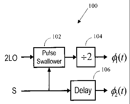
The synthesizer 100 presented in Figure 6 uses an input square wave (2L0)
at twice the frequency of the RF carrier of the signal being modified by a
signal
denoted as S. Signal S could be the signal being modified, provided the
criteria for
the cp, and cp2 signals are met, though generally it will be an independently
generated
control signal. This control signal S could also be generated using a delta-
sigma (A -
S) modulator which is known in the art.
A pulse swallower 102 is then used to remove pulses from the 2L0 square
wave. The pulse swallower 102 is controlled by the input signal S, such that
when
the input signal, S, switches state, a pulse is removed from the 2L0 signal.
The
resulting signal is then passed through a divide-by-2 circuit 104 to produce
the cp,(t)
output signal. The input signal S passes through a delay circuit 106 which
delays it
by the amount of time it takes the 2L0 signal to propagate through to the
cp,(t)
output, so that the two signals are synchronized. The output of this delay
circuit 106
is the cp2(t) mixer signal.
Assuming that the input signal S follows no regular pattern, the output
signals
cp,(t) and cpz(t) could be random or pseudo-random. Since this circuit uses an
oscillator at twice the carrier frequency of the input signal, there is no LO
signal to
leak to the output or into other parts of the circuit. Similarly, none of the
intermediate
signals, nor either of the mixer signals cp, and cpz, has an LO frequency
component.
A logic circuit that performs the function of Figure 6 is presented in Figure
7.
The pulse swallower 102 consists of a standard delay latch (D-latch) Dl. A D-
latch
is a flip-flop whose input passes to the output after one clock cycle. The
triggering of
the pulse swallower 102 is controlled by D-latches D4 through D7 and the
exclusive
OR (XOR) gate XOR1, which detect the leading edge of the input signal S and
SUBSTITUTE SHEET (RULE 26)
CA 02381999 2002-02-13
WO 01/17122 PCT/CAOO/00996
-15-
create a pulse which causes Dl to swallow a pulse of the input signal 2L0.
D-latches D2 and D3 form a divide-by-two circuit 104 that receives the output
of Dl
and produces the cp, mixing signal. The D-latches D4 through D7 also delay the
S
signal to produce the cpz signal. Note that this circuit produces both the I
and Q
components of cp, and cpz, which would be required for input to a mixer such
as that
of Figure 5; subscripts indicate the signals required for the frequency
translation of
the in-phase and quadrature components of the input signal S, respectively.
Figure 8 presents another method for producing the signals cp, and T2. Here,
the D-latches D8 through D13 form a shift register which is clocked by the
signal
2L0. The signal 2L0 is once again a square wave that has a frequency of twice
the
RF carrier frequency. The shift register can be initially loaded with a
predetermined
sequence and the output cp, will cycle through that sequence producing the
desired
output. The second output cpz is then produced by taking the output of
consecutive
taps from the shift register, and exclusive-ORing them together with gate XOR2
to
produce a signal that can be used to clock a second shift register (D14 and
D15).
The output of the second shift register is then 92.
Figure 9 shows a method similar to that of Figure 8, except that signal cpZ is
generated by a second shift register (D22 through D27), which is a duplicate
of the
shift register that produces the signal cp, (D16 through D21). As well, there
is a
difference in the initial loading of the shift registers; the first shift
register being
loaded with the sequence that will produce cp,, and the second being loaded
with the
sequence which will produce cp2.
The previous methods of generating cp, and cp2 use an input signal at twice
the RF carrier frequency (that is, 2L0). In some situations it may be
difficult to
design logic to operate at this frequency. If enough isolation can be obtained
to
protect an input of LO from leaking into the RF band, the method shown in
Figure 10
can be used.
Here the edges of the input signal S are aligned with the LO input edges
through the D flip-flop D28. The inverter 11 adds a delay to the LO input to
make
sure the two signal edges remain aligned. The two signals are then passed
through
an exclusive OR (XOR) gate XOR3 to produce the output signal cQ,. Another
delay is
added to the output of the D28 latch via invertor 12 to keep the edges aligned
with
the output of the XOR gate XOR3. The output of 12 is then cpZ.
SUBSTITUTE SHEET (RULE 26)
CA 02381999 2002-02-13
WO 01/17122 PCT/CAOO/00996
- 16-
The signal cp2 can also be generated by using a shift register with feedback
similar to those used in the generation of PN sequences for use in spread-
spectrum
communications. An example of such a shift register is shown in Figure 11. The
D-latches D29 through D32 form a shift register which is clocked by the signal
at
twice the RF carrier frequency. MOD1 does a modulo-2 multiplication of the
output
of D31 with the output of D32, which is then fed into the input of D32 to
produce the
required feedback. The signal cpz is then produced at the output of D32. A
similar
shift register with similar feedback can be used to produce the signal cp,.
The
conditions on the design of these shift registers are that they produce the
signals cp,
and cpz that have the properties mentioned above:
= cp,(t) * cpz(t) must have a frequency component at the RF carrier frequency;
= cp,(t) * 92(t) must not contain a significant amount of power at frequencies
other that the RF carrier frequency; and
= cp,(t) and cpz(t) must not contain a significant amount of energy in the RF
signal bandwidth.
The signals of the invention may also be generated in many other ways,
which would be clear from the teachings herein. For example, cp, could be
generated using a control signal S to selectively divide a 2L0 signal by
either 2 or by
4. In this case, if the value of S is a digital "0" then the 2L0 signal could
be divided
by 2, and if the value of S is a digital "1 ", the 2L0 signal could be divided
by 4. The
function cpZ can be derived from the control signal S in a similar manner, to
generate
a pair of time-varying signals which meet the criteria of the invention to the
extent
required by the application.
The invention allows one to fully integrate a RF transmitter on a single chip
without using external filters, while furthermore, the RF transmitter can be
used as a
multi-standard transmitter.
The construction of the necessary logic to generate the mixing signals of the
invention would be clear to one skilled in the art from the description
herein. Such
signals may be generated using basic logic gates, field programmable gate
arrays
(FPGA), read only memories (ROMs), micro-controllers or other devices known in
the art. Though the figures herein imply the use of analogue components, all
embodiments can be implemented in digital form.
It would be clear to one skilled in the art that many variations may be made
to
the designs presented herein, without departing from the spirit of the
invention. One
such variation to the basic structure in Figure 3 is to add a filter between
the two
SUBSTITUTE SHEET (RULE 26)
CA 02381999 2002-02-13
WO 01/17122 PCT/CAOO/00996
-17-
mixers 72 and 74 to remove unwanted signals that are transferred to the output
port.
This filter may be a low pass, high pass, or band pass filter depending on the
transmitter requirements, and may be purely passive, or have active
components.
In Figure 3, two mixer signals are used to perform the down-conversion or
up-conversion of x(t). It is also possible to use more than two signals to
accomplish
the same goal. The block diagram of Figure 12 presents such a variation, where
several functions cp,, cp2, cp3 ... cpn are used to generate the virtual LO.
Here, cp,'' cp2*...
"cpn has a significant power level at the LO frequency being emulated, but
each of
the functions cp,... cpn contain an insignificant power level at LO. Each of
these
methods of signal generation can be easily extended to produce more than two
signals.
The electrical circuits of the invention may be described by computer
software code in a simulation language, or hardware development language used
to
fabricate integrated circuits. This computer software code may be stored in a
variety
of formats on various electronic memory media including computer diskettes, CD-
ROM, Random Access Memory (RAM) and Read Only Memory (ROM). As well,
electronic signals representing such computer software code may also be
transmitted via a communication network.
Clearly, such computer software code may also be integrated with the code
of other programs, implemented as a core or subroutine by external program
calls,
or by other techniques known in the art.
The embodiments of the invention may be implemented on various families of
integrated circuit technologies using digital signal processors (DSPs),
microcontrollers, microprocessors, field programmable gate arrays (FPGAs), or
discrete components. Such implementations would be clear to one skilled in the
art.
The invention may be applied to various communication protocols and
formats including: amplitude modulation (AM), frequency modulation (FM),
frequency
shift keying (FSK), phase shift keying (PSK), cellular telephone systems
including
analogue and digital systems such as code division multiple access (CDMA),
time
division multiple access (TDMA) and frequency division multiple access (FDMA).
The invention may be applied to such applications as wired communication
systems include computer communication systems such as local area networks
(LANs), point to point signalling, and wide area networks (WANs) such as the
Internet, using electrical or optical fibre cable systems. As well, wireless
communication systems may include those for public broadcasting such as AM and
SUBSTITUTE SHEET (RULE 26)
CA 02381999 2002-02-13
WO 01/17122 PCT/CAOO/00996
-18-
FM radio, and UHF and VHF television; or those for private communication such
as
cellular telephones, personal paging devices, wireless local loops, monitoring
of
homes by utility companies, cordless telephones including the digital cordiess
European telecommunication (DECT) standard, mobile radio systems, GSM and
AMPS cellular telephones, microwave backbone networks, interconnected
appliances under the Bluetooth standard, and satellite communications.
While particular embodiments of the present invention have been shown and
described, it is clear that changes and modifications may be made to such
embodiments without departing from the true scope and spirit of the invention.
SUBSTITUTE SHEET (RULE 26)