Note: Descriptions are shown in the official language in which they were submitted.
CA 02384001 2002-02-28
SPECIFICATION
Light Emitting Block
TECHNICAL FIELD
This invention relates to light emitting blocks laid on
side wall surfaces of garages, gardens and roads, or on wall
surfaces of buildings and houses.
to BACKGROUND ART
As one type of blocks laid on side wall surfaces
provided for garages, gardens and roads, or on wall surfaces
of buildings and houses, light collecting blocks are known,
which are formed of transparent or translucent glass to take
in sunlight from the ambient.
Conventionally, side wall surfaces of a garage or wall
surfaces of a house have light collecting blocks arranged in
positions where it is desired to take in sunlight from the
ambient, and ordinary blocks arranged in other positions.
During the daytime, ambient sunlight is allowed to pass
through and taken in by the light collecting blocks to aid in
illuminating the interior of the garage, building or house, to
help in activities in the garage, building or house. However,
during the nighttime, no sunlight is available from the
ambient and the garage or house interior cannot be
-1-
CA 02384001 2002-02-28
illuminated.
That is, the light collecting blocks as the conventional
blocks are not effectively used when there is no sunlight
from the ambient as at nighttime.
Having regard to the state of the art noted above, the
object of this invention is to provide light emitting blocks
excellent in response to emergency situations as well as
workability, maintainability and design.
to DISCLOSURE OF THE INVENTION
A light emitting block according to this invention is
characterized by containing solar batteries arranged to
receive sunlight penetrating a block surface portion to
generate an electromotive force, an electric double layer
capacitor for storing electric power generated by the solar
batteries, a light emitting device disposed with a light
emitting surface thereof opposed to a reverse surface of a
block surface portion from which light is to be emitted, and
an emission control device operable, when ambient
2o illuminance is below a predetermined illuminance level, for
automatically supplying the electric power stored in the
electric double layer capacitor to the light emitting device to
illuminate the light emitting surface of the light emitting
device.
Such a light emitting block is applied to an attaching
-2-
CA 02384001 2002-02-28
surface such as a Side wall of a garage or a wall of a house.
After application, sunlight passes through translucent
regions of the block surface portion of the light emitting
block, and strikes on the solar batteries. The solar
batteries having received the sunlight generate electric
power, and accumulate the electric power in the electric
double layer capacitor at the same time.
When ambient illuminance falls below the predeter-
mined illuminance level toward the evening, the emission
control device automatically supplies the power stored in the
double layer capacitor to the light emitting device, whereby
the light emitting surface of the light emitting device begins
to shine. The light emitted from the light emitting surface
passes through the translucent regions of the block surface
portion to radiate from the block to the ambient. In this
way, the light emitting block performs a light emitting
function.
That is, the light emitting block of this invention has
an in-system power generating function provided by the
2o solar batteries and electric double layer capacitor. All that
is required is to lay the light emitting block in place. There
is no need for a wiring operation or a subsequent checking
operation. Moreover, there is no possibility of light
emission stoppage in time of power failure due to a natural
disaster or the like. The light emitting function is firmly
-3-
CA 02384001 2002-02-28
maintained.
Thus, the light emitting block according to this inven-
tion has an appropriate in-system power generating function
provided by the solar batteries and electric double layer
capacitor. There is no need for a wiring operation or a sub-
sequent checking operation, to realize improved workability
and maintainability. Moreover, there is no possibility of
light emission stoppage in time of unexpected power failure
due to a natural disaster or the like, which provides
improved response to emergency situations.
In the light emitting block of this invention, the light
emitting device preferably comprises a planar light emitting
device or a point light emitting device.
The light emitting device comprising a planar light
emitting device as noted above is not too dazzling or
offensive to view, which provides an improvement in design
over the prior art. The light emitting device comprising a
point light emitting device emits light farther than the
planar light emitting device.
In the light emitting block of this invention, the planar
light emitting device preferably has a transparent plate dis-
posed parallel to the block surface portion, a light projecting
device for injecting light from end surfaces of the
transparent plate into the transparent plate along a
direction of a plane thereof, a light scattering device with a
-4-
CA 02384001 2004-12-17
73454-18
surface of the transparent plate close to the block surface
portion acting as a light scattering surface, and a light
reflecting device with a surface of the transparent plate
remote from the block surface portion acting as a light
reflecting surface.
In time of light emission, the light injected by
the light projecting device into the transparent plate along
the direction of the plane thereof is reflected and
deflected toward the block surface portion by the light
reflecting surface on the reverse side. Then, the light,
while being scattered by the light scattering surface on the
front side, radiates to the ambient from the translucent
regions of the block surface portion. Since a large part of
incident light is released after the reflection from the
light reflecting surface, the light emitting surface is
bright. The light emitting surface gives a very mellow
(soft) impression as a result of the light scattering action
(light diffusion) of the light scattering surface.
In accordance with a broad aspect, the invention
provides a light emitting block comprising a transparent or
translucent block body containing: solar batteries arranged
to receive sunlight penetrating a block surface portion to
generate an electromotive force; an electric double layer
capacitor for storing electric power generated by the solar
batteries; light emitting means disposed with a light
emitting surface thereof opposed to a reverse surface of a
block surface portion from which light is to be emitted; and
emission control means operable, when ambient illuminance is
below a predetermined illuminance level, for automatically
supplying the electric power stored in the electric double
layer capacitor to the light emitting means to illuminate
the light emitting surface of the light emitting means.
- 5 -
CA 02384001 2004-12-17
73454-18
BRIEF DESCRIPTION OF THE DRAWINGS
Fig. 1 is a plan view of a light emitting block in
a first embodiment seen from solar batteries;
Fig. 2 is a sectional view showing an interior
structure of the light emitting block in the first
embodiment;
Fig. 3 is a plan view of the light emitting block
in the
- 5a -
r.
CA 02384001 2002-02-28
first embodiment seen from a planar light emitting device;
Fig. 4 shows an electric circuit of the light emitting
block in the first embodiment;
Fig. 5 is a plan view showing a construction of a planar
light emitting member of the light emitting block in the first
embodiment;
Fig. 6 is a side view showing the construction of the
planar light emitting member of the light emitting block in
the first embodiment;
to Fig. 7 is a schematic view showing light reflections in
the planar light emitting member of the light emitting block
in the first embodiment;
Fig. 8 is a plan view of a light emitting block in a
second embodiment seen from a point light emitting device;
Fig. 9 is a sectional view showing an interior structure
of the light emitting block in the second embodiment;
Fig. 10 is a plan view of a light emitting block in a
third embodiment seen from solar batteries;
Fig. 11 is a sectional view showing an interior
2o structure of the light emitting block in the third
embodiment;
Fig. 12 is a plan view of a light emitting block in a
fourth embodiment seen from solar batteries;
Fig. 13 is a sectional view showing an interior
structure of the light emitting block in the fourth
-6-
s
CA 02384001 2002-02-28
embodiment; and
Fig. 14 is a plan view showing a display sheet
employed in a modified light emitting block.
BEST MODE FOR CARRYING OUT THE INVENTION
Modes for solving the problem of the prior art include
the following:
<First Embodiment>
The first embodiment will be described with reference
to to the drawings. Fig. 1 is a plan view of a light emitting
block in the first embodiment seen from solar batteries, Fig.
2 is a view in vertical section showing an interior structure
of the light emitting block in the first embodiment, Fig. 3 is
a plan view of the light emitting block in the first
embodiment seen from a light emitting device, and Fig. 4 is
a circuit diagram showing an electric circuit of the light
emitting block in the first embodiment.
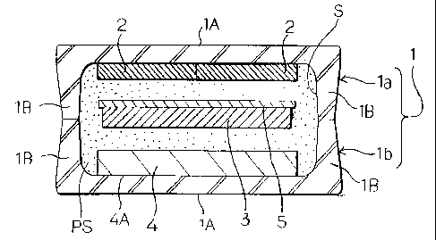
As shown in Figs. 1 through 3, the light emitting block
in the first embodiment includes a main block body 1 formed
of a first and a second boxes 1a and lb, and a light emitting
functional portion.
As shown in Fig. 2, the main block body 1 has the first
and second boxes 1a and lb formed of transparent glass and
having a square shape, with respective openings opposed to
each other. The first and second boxes 1a and lb have the
-7-
r
CA 02384001 2002-02-28
same configuration, with bottom walls thereof acting as
plate-like block surface portions lA. Side walls of the first
and second boxes la and lb act as legs 1B for supporting the
block surface portions lA. Since the first and second boxes
la and lb are formed of transparent glass, the entire block
surface portions lA of the first and second boxes 1a and lb
act as translucent regions.
The light emitting block in the first embodiment is
embedded, with a block surface portion 1A exposed, in a
to desired location such as a side wall of a garage or an interior
wall of a house. The block surface portion 1A constitutes a
wall surface. Numerous light emitting blocks may be ar-
ranged in a matrix form, or only a single light emitting block
may be used on its own.
The light emitting functional portion will be described
next.
This light emitting functional portion includes compo-
nents necessary to perform a light emitting function, and is
disposed in an interior space of main block body 1. The
components necessary to perform the light emitting function
are stored in a space S formed in the back of the block
surface portions 1A by the plate-like block surface portions
lA and legs 1B.
Specifically, as shown in Figs. 1 through 3, the space S
of the block surface portions lA accommodates solar
.g_
CA 02384001 2002-02-28
batteries 2 for generating electric power for light emission,
an electric double layer capacitor 3 for storing the power
generated by the solar batteries 2, a planar light emitting
member 4 for radiating light from surfaces of the block
surface portions lA to the ambient, and a printed board 5
having an emission control circuit for lighting the planar
light emitting member 4.
During the daytime when sunlight pours down, the
power generated by the solar batteries 2 accumulates in the
l0 electric double layer capacitor 3. On the other hand, when
it grows darker toward the evening with the sun setting, the
power stored in the electric double layer capacitor 3 is sup-
plied to the planar light emitting member 4. Then, a light
emitting surface 4A of the planar light emitting member 4
automatically emits light, causing the block to shine.
In the light emitting block in the first embodiment, the
solar batteries 2 which receive sunlight from the ambient
are disposed directly under the block surface portion lA of
the first box la, and the planar light emitting member 4
which releases light to the ambient is disposed directly
under the block surface portion lA of the second box lb.
The electric double layer capacitor 3 and printed board 5
having no immediate relationship with the ambient are
arranged between the solar batteries 2 and planar light
emitting member 4.
-9-
CA 02384001 2002-02-28
The components of the light emitting block in the first
embodiment will be described in detail hereinafter.
In the first embodiment, the space S in the back of the
block surface portions lA of the first and second boxes la
and lb is made fully waterproof with a resin sealing, which
is achieved by filling a waterproof resin PS through the
openings after the components necessary for the light
emitting function are mounted in place. Thus, when the
light emitting block in the first embodiment is applied to a
l0 wall surface, the components in the space S of the block
surface portions 1A are protected from moisture and water.
As shown in Fig. 1, the light emitting block in the first
embodiment has two solar batteries 2 placed substantially
throughout the block surface portion lA of the first box la,
in a series arrangement for receiving sunlight penetrating
the block surface portion lA to generate electromotive forces
simultaneously. In the first embodiment, each solar
battery 2 includes seven unit cells 2a connected in series.
Of course, the number of unit cells in each solar battery 2 is
not limited to a particular number. A suitable number, one
or more, is selected according to a voltage required of each
solar battery 2.
In the light emitting block in the first embodiment, as
shown in Fig. 4, the solar batteries 2 are connected in series
to the electric double layer capacitor 3, and the power
-l0-
CA 02384001 2002-02-28
generated by each solar battery 2 is stored in the electric
double layer capacitor 3. The light emitting block in the
first embodiment is used on a wall surface or the like, and
therefore foreign objects such as fallen leaves or waste paper
about to adhere to the block surface portion will fall by
gravity. There is hardly any possibility that the solar
batteries 2 are partly covered with foreign objects. Thus,
sufficient power may be stored since contamination of the
block will not affect the power storing function. The solar
l0 batteries 2 may therefore be connected in series to provide
an increased voltage required.
Three or more solar batteries 2 may be used to form a
series/parallel connection according to a voltage required,
instead of connecting all the solar batteries 2 in series.
Though only one electric double layer capacitor 3 is shown in
Fig. 4, a plurality of such capacitors may be connected in
parallel according to an electrostatic capacity needed.
A total quantity of power generated by the above solar
batteries 2 is determined to cope with a small quantity of
2o solar radiation during the daytime in a spell of cloudy or
rainy weather. Thus, even in such conditions, the electric
double layer capacitor 3 is charged with electric power to be
consumed by a load for the day. The electric double layer
capacitor 3 has a capacity for storing at least the quantity of
electric power consumed by the load in a day. Thus, the
-11-
4
CA 02384001 2002-02-28
capacity of electric double layer capacitor 3 provides a
margin 1/5 to 1/30 of a conventional storage battery. The
electric double layer capacitor 3 is much smaller and lighter
than the conventional storage battery.
In the first embodiment, as shown in Fig. 4, an
overvoltage protection circuit 6, a reverse flow preventive
diode 7 and a voltage stabilizer circuit 8 are connected
between the solar batteries 2 and electric double layer
capacitor 3.
The overvoltage protection circuit 6 is provided to
prevent the charging voltage of solar batteries 2 from reach-
ing an overcharging voltage in excess of a permissible
voltage. During the nighttime when no electromotive force
is generated by the solar batteries 2, power could
inadvertently flow from the electric double layer capacitor 3
having a high voltage back to the solar batteries 2. The
reverse flow preventive diode 7 prevents such a reverse flow
of the power stored in the electric double layer capacitor 3.
The voltage stabilizer circuit 8 prevents variations in the
charging voltage and maintains it constant.
Where sunshine is stable to render voltage generation
relatively stable, one or both of the reverse flow preventive
diode 7 and voltage stabilizer circuit 8 may be omitted.
This will simplify the construction.
On the other hand, as shown in Fig. 5, the planar light
-12-
CA 02384001 2002-02-28
emitting member 4 has a transparent plate 4B disposed par-
allel (i.e. opposed surfaces being parallel) to the block
surface portion lA, and eight light emitting diodes (LEDs)
4E-4L for injecting light from a pair of opposite end surfaces
4C and 4D of the transparent plate 4B into the transparent
plate 4B along a direction of a plane thereof. The
transparent plate 4B has a surface 4M opposed to the block
surface portion lA and acting as a light scattering surface.
The transparent plate 4B has a surface (reverse surface) 4N
l0 remote from the block surface portion lA, which acts as a
light reflecting surface.
The light emitting diodes 4E-4H and light emitting
diodes 4I-4L are distributed to and arranged on the end sur-
face 4C and the end surface 4D, such that light enters the
transparent plate 4B in coinciding directions as shown in
dot-and-dash lines in Fig. 5. These light emitting diodes
4E-4L are inserted and fixed in bores formed in elongate,
white opaque resin pieces 4a and 4b placed in close contact
with the end surfaces 4C and 4D of transparent plate 4B.
Where irregularity occurs with the light emission from
the light emitting surface 4A, the irregularities may be sup-
pressed by arranging the light emitting diodes 4E-4H and
light emitting diodes 4I-4L alternately. On the other hand,
where no light emission irregularity occurs or light emission
irregularity presents no problem in use, only those on one
-13-
a
CA 02384001 2002-02-28
side may be provided, of the light emitting diodes 4E-4H and
4I-4L arranged on the opposite sides.
In the first embodiment, the transparent plate 4B is in
the form of a colorless, transparent acrylic plate. The light
scattering surface (light scattering device) is formed by
sand-blasting the surface 4M, while the light reflecting
surface, as shown in Fig. 6, is formed by laminating a white
coating 40 (light reflecting device) and a white sheet 4P
(light reflecting device) on the reverse surface 4N.
1o The light scattering surface may be formed by laminat-
ing a light scattering sheet (light scattering device) on the
surface 4M. The light reflecting surface may also be formed
by applying a metal film to the reverse surface 4N, or lami-
nating a mirror sheet thereon for mirror reflection of
incident light.
Further, the end surfaces 4C and 4D of transparent
plate 4B act as reflecting surfaces which are provided by
white surfaces of opaque resin pieces 4a and 4b. The two
remaining end surfaces of transparent plate 4B also are
2o made reflecting surfaces such as by forming white coatings
(not shown) thereon. Of course, each end surface of
transparent plate 4B may define a reflecting surface having
a metallic mirror layer or the like.
When the light emitting diodes 4E-4L are lit, as shown
in Fig. 7, the light entering the transparent plate 4B from
-14-
1
CA 02384001 2002-02-28
the light emitting diodes 4E-4L is reflected by the light
reflecting surface defined by the reverse surface 4N to travel
toward the block surface portion lA. The light radiates
from the block surface portion lA to the ambient while being
scattered by the light scattering surface defined by the
surface 4M. Since the planar light emitting member 4 is a
planar light emitter, the light emitting surface 4A is mellow
and pleasing to the eye. Since a large part of incident light
is released after being reflected by the light reflecting
to surface, the light emitting surface 4A is bright. The light
emitting surface 4A gives a very mellow impression as a
result of the light scattering function (light diffusion) of the
light scattering surface.
The light emitting diodes 4E-4L of planar light
emitting member 4 are operable under the following lighting
control by an emission control circuit 9.
When ambient illuminance L is found equal to or below
a predetermined illuminance Lon, the emission control
circuit 9 supplies the power stored in the electric double
layer capacitor 3 to the light emitting diodes 4E-4L of planar
light emitting member 4. Conversely, when ambient
illuminance L is found equal to or above a predetermined
illuminance Loff, the emission control circuit 9 stops the
power supply to the light emitting diodes 4E-4L. In the
first embodiment, the electromotive force of solar batteries 2
-15-
CA 02384001 2002-02-28
is used as a detection signal indicative of ambient
illuminance L. The solar batteries 2 act also as optical
sensors, and the electromotive force of solar batteries 2 is in
a proportional relationship to ambient illuminance. It is
therefore possible to utilize the electromotive force of solar
batteries 2 in determining whether the ambient illuminance
L is in the illuminance (darkness) level for causing the light
emitting block to emit light or not.
The emission control circuit 9 in the first embodiment
l0 has the predetermined illuminance Lon for starting the
power supply, which is slightly lower than the
predetermined illuminance Loff for stopping the power
supply. If the same illuminance were set for starting and
stopping the power supply, a chattering phenomenon would
occur to repeat starting and stopping of the power supply
frequently in response to slight illuminance variations. To
avoid such chattering phenomenon, what is known as
hysteresis property is provided, whereby the power supply is
not stopped after it is started at the predetermined
2o illuminance Lon, unless the ambient illuminance L
increases to the slightly higher illuminance Loff.
As shown in Fig. 4, the accumulated power is supplied
from the electric double layer capacitor 3 to anodes of light
emitting diodes 4E-4L via a booster circuit 10, and cathodes
of light emitting diodes 4E-4L are connected to a common
-16-
CA 02384001 2002-02-28
line (grounding line) through switching elements SW1 and
SW2. When the accumulated power is supplied, the
emission control circuit 9 turns on the switching elements
SW1 and SW2 whereby currents flow to the light emitting
diodes 4E-4L to light the latter. The operation frequency
for turning on the switching elements SW1 and SW2 is 60Hz
(hertz), for example. The light emitting diodes 4E-4L emit
light with this operation frequency.
In the first embodiment, the switching elements SW1
l0 and SW2 are alternately turned on in a short time for power
saving purposes. That is, the light emitting diodes 4E-4L
blink at high speed. This presents no problem since light
emission appears to occur continuously in the human eye
due to afterglow.
The switching elements SW1 and SW2 may be in the
form of transistors, for example. Where the light emitting
diodes have a low rated voltage, the booster circuit 10 may
be omitted so that the electric double layer capacitor 3
supplies the accumulated power directly to the light
emitting diodes. Alternatively, the booster circuit 10 may
be formed of a DC-DC converter to effect a negative boosting,
i.e. step-down, to lower the voltage.
The light emitting block in the first embodiment has,
mounted en bloc on the printed board 5, the overvoltage pro-
tection circuit 6, reverse flow preventive diode 7, voltage sta-
-17-
CA 02384001 2002-02-28
bilizer circuit 8, emission control circuit 9, switching
elements SW1 and SW2 and booster circuit 10, as well as
the electric double layer capacitor 3.
Operation of the light emitting block in the first em-
bodiment having the above construction will be described
hereinafter.
During the daytime when the sun is up, each solar bat-
tery 2 receiving sunlight generates electric power and trans-
mits it to the electric double layer capacitor 3. As a result,
l0 power accumulates in the electric double layer capacitor 3.
Ambient illuminance is high during the daytime, and the
emission control circuit 9 maintains the switching elements
SW1 and SW2 turned off. Thus, the light emitting diodes
4E-4L are maintained in off state with no current flowing
thereto. The light emitting surface 4A does not shine at all.
Ambient illuminance L gradually lowers toward the
evening. When ambient illuminance L falls to or below the
predetermined illuminance Lon, the emission control circuit
9 alternately turns on the switching elements SW1 and SW2.
Thus, currents flow to the light emitting diodes 4E-4L to
light the latter. The light emitting surface 4A begins to
shine to set the light emitting block to a state of light
emission.
During the nighttime when the sun is sunk low,
ambient illuminance L remains below the illuminance Lon
18-
CA 02384001 2002-02-28
and the light emitting block continues to maintain the
emission state.
Toward daybreak, ambient illuminance L increases
gradually. When ambient illuminance L returns to the pre-
y determined illuminance Loff slightly higher than the prede-
termined illuminance Lon, the emission control circuit 9
turns off the switching elements SW1 and SW2 again. The
currents stop flowing to the light emitting diodes 4E-4L to
turn off the latter. Thus, the light emitting surface 4A
1o stops shining, and the light emitting block switches to a
non-emission state.
As described above, the light emitting block in the first
embodiment has an appropriate in-system power generating
function provided by the solar batteries 2 and electric double
15 layer capacitor 3. There is no need for a wiring operation
or a subsequent checking operation, to realize improved
workability and maintainability. Moreover, the light
emitting block continues to emit light even in time of
blackout, which provides improved response to emergency
2o situations. The planar light emitting member 4, as it is
planar, is not too dazzling or offensive to view, which
provides an improvement in design.
This invention is not limited to the first embodiment
described above, but may be modified as follows:
25 (1) In the light emitting block in the first embodiment
-19-
a
CA 02384001 2002-02-28
described above, the light emitting device comprises the
planar light emitting member 4 acting as a planar light
emitting device. In a modification, as shown in Figs. 8 and
9, the light emitting device may comprise a point light
emitting device. This modification will be described
hereinafter as a second embodiment.
<Second Embodiment>
The point light emitting device is realized by placing
light emitting diodes 4E-4L in mounting bores 12a formed in
to a plate 12. With the light emitting block in this second em-
bodiment, the light emitting diodes 4E-4L emit light to
shine directly upon a target location, and therefore to reach
farther than the light from the planar light emitting device
in the first embodiment. Thus, the light reflecting device
and light scattering device used in the first embodiment
may be dispensed with.
The mounting bores 12a formed in the plate 12 of the
point light emitting device may be formed at an angle,
instead of perpendicular, to the surface of plate 12
2o contacting the block surface portion lA, or the plate 12 per
se may be disposed at an angle to the block surface portion
lA. In this way, light may be emitted in different
directions to irradiate different locations. An area around
the feet may be illuminated, for example.
(2) In the light emitting block in the first embodiment,
-20-
~E
CA 02384001 2002-02-28
the light emitting diodes 4E-4L are turned on at 60Hz
(hertz). Instead, light emission may be performed at a
frequency below 60Hz (hertz), so that the intermittent light
emission is perceptible to the human eye.
(3) In the light emitting block in the first embodiment,
the solar batteries 2 and the planar light emitting member 4
acting as the light emitting device are placed substantially
throughout the block surface portions, respectively. In a
modification, as shown in Figs. 10 and 11, the solar batteries
l0 2 and planar light emitting member 4 may be reduced in
area, compared with the block surface portions. This
modification will be described hereinafter as a third
embodiment.
<Third Embodiment>
Light collecting portions 13 are formed in the space
produced as a result of diminishing the solar batteries 2 and
planar light emitting member 4. These light collecting por-
tions 13 are formed, for example, by filling a translucent
resin, or by being left completely hollow.
In the daytime the solar batteries 2 at the block
surface portion 1A receive sunlight and generate electric
power. The power is stored in the electric double layer
capacitor 3. Ambient sunlight passes to be collected
through the parts of block surface portions 1A not blocked by
the solar batteries 2 or planar light emitting portion 4 to aid
-21-
CA 02384001 2002-02-28
in illuminating a garage interior, building interior or house
interior.
When ambient illuminance L falls to or below the
predetermined illuminance in the evening, the emission
control device automatically supplies the power stored in the
electric double layer capacitor 3 to the planar light emitting
member 4. Then, the light emitting surface of planar light
emitting member 4 begins to shine. The light exiting the
light emitting surface passes through the block surface por-
to tion lA to be released to areas around the light emitting
block, thereby fulfilling the light emitting function of the
light emitting block.
(4) In the light emitting block in the above third em
bodiment, as shown in Figs. 10 and 11, the solar batteries 2
and planar light emitting portion 4 have a smaller area than
the block surface portions. In a modification, as shown in
Figs. 12 and 13, the solar batteries 2 comprise the
semi-transmission type for transmitting part of incident
sunlight, and the planar light emitting member 4 acting as
the light emitting device has a smaller area than the block
surface portions 1A. This modification will be described
hereinafter as a fourth embodiment.
<Fourth Embodiment>
Light collecting portions 13 are formed in the space
produced as a result of diminishing the planar light emitting
-22-
4
CA 02384001 2002-02-28
member 4. These light collecting portions 13 are formed,
for example, by filling a translucent resin, or by being left
completely hollow.
In the daytime the semi-transmission type solar bat-
s teries 2 at the block surface portion lA intercept part of sun-
light and generate electric power. The power is stored in
the electric double layer capacitor 3. The sunlight not
intercepted by the semi-transmission type solar batteries 2
passes through the light collecting portions 13 to be taken
l0 into a garage, building or house to aid in illuminating the
interior of the garage, building or house.
When ambient illuminance L falls to or below the
predetermined illuminance in the evening, the emission con-
trol device automatically supplies the power Stored in the
15 electric double layer capacitor 3 to the planar light emitting
member 4. Then, the light emitting surface of planar light
emitting member 4 begins to shine. The light exiting the
light emitting surface passes through the block surface por-
tion lA to be released to areas around the light emitting
20 block, thereby fulfilling the light emitting function of the
light emitting block.
(5) The light emitting block in the first embodiment
uses the planar light emitting member 4 of the light
emitting diode type. In a modification, the planar light
25 emitting member 4 may be formed of an EL
-23-
CA 02384001 2002-02-28
(electro-luminescence) element. Further, the planar light
emitting member may be formed of a cold-cathode tube or
xenon tube.
(6) The light emitting block in the first embodiment
may be modified such that, where the charging voltage of
electric double layer capacitor 3 is insufficient, a further
solar battery or batteries 2 may be connected in series to
increase the charging voltage, or where the electric double
layer capacitor 3 has an insufficient voltage endurance,
to electric double layer capacitors 3 may be connected in series
to increase the voltage endurance.
(7) In the light emitting block in the first embodiment,
the entire block surface portion 1A provides a translucent
region. The entire block surface portion lA need not
provide a translucent region, but only a necessary part
thereof may provide a translucent region.
(8) In the light emitting block in the first embodiment,
the first and second boxes la and lb have the same
configuration. For example, one of them may be in the
2o form of a square box, and the other in a complete plate form.
The first and second boxes 1a and lb may be shaped in any
way as long as they may be installed in place with the
components necessary for the light emitting function sealed
inside. While the first and second boxes la and 1b are
formed of transparent glass, they may be formed of a resin
-24-
CA 02384001 2002-02-28
or may be colored with transparency.
(9) The light emitting block in the first embodiment
may be modified to include a display plate 11 (display mem-
ber) as shown in Fig. 14, which is laminated on the light
emitting surface 4A.
The display plate 11 defines an arrow mark formed by
combining an arrow-shaped transparent region lA (light
transmitting region) with a black region 11B (light shielding
region). The arrow mark may be recognized at night owing
to the light emitting function of the light emitting block.
The display plate 11 has the reverse side of light
shielding region 11B formed as a mirror surface. All light
radiates from the transparent region 1A without being
absorbed by the black region 11B. This results in an out-
standing difference in light quantity between the
transparent region 1A and black region 11B to render the
arrow mark clearly visible. This modified light emitting
block has, besides the light emitting function, a displaying
function based on the arrow mark serving as a display.
The type of display is of course not limited to the arrow
mark. Instead of laminating the display plate 11, a display
may be painted on the light emitting surface 4A.
(10) The light emitting blocks of this invention are
not limited in application to embedment in side wall
surfaces of garages, gardens and roads, or in wall surfaces of
-25-
~4
CA 02384001 2002-02-28
buildings and houses. The blocks may be placed on at least
part of a fence at a construction site, for example. This
allows the construction fence to be located readily at night.
INDUSTRIAL UTILITY
As described above, this invention is suited for applica-
tion to light emitting blocks used on side wall surfaces of
garages, gardens and roads, or on the wall surfaces of build-
ings and houses.
-26-