Note: Descriptions are shown in the official language in which they were submitted.
Method and device for the electrolytic treatment of electrically conducting
surfaces separated plates and film material pieces in addition to uses of said
method
Description
The invention relates to a method and device for electrolytic treatment of
electrically conductive surfaces of mutually isolated sheet and foil material
pieces and applications of the method, especially for producing circuit
boards and conductive foils.
Electroplating processes are used to produce circuit boards and
conductive foils in order either to deposit metal or to implement other
electrolytic treatments, for example metal etching methods. For quite a
number of years, so-called continuous system have been used for this
purpose, the material being transported through said systems in a
horizontal direction and, during transportation, being brought in contact
with treatment fluid.
Such a continuous system is described for example in DE 36 234 481 A1.
This unit has anodes, current supplies to the circuit boards to be coated
and conveying means. The conveying means are configured as a
continuous, revolving actuated row of individual clamps which hold the
lateral edges of the circuit boards securely and move in the conveying
direction. Current is supplied to the circuit boards via these clamps. For
this purpose, the clamps are provided with current via brush
arrangements.
Another type of electric contact and way of conveying circuit boards in a
continuous system is described in DE 32 36 545 C3. In this case, contact
wheels are used instead of clamps, said wheels rolling on the moved
circuit boards and providing electrical contact with the circuit boards in
this way.
CA 02384249 2002-03-06
' ~ 2
Both systems must be elaborately constructed in order to be able to
transfer the at times large metallising currents to the circuit boards. In
the case of very high metallising currents, there are still no satisfactory
solutions since fundamentally contact resistances occur at the contacts
(clamps, contact wheels) so that the contact points can be heated to a very
high degree from time to time by the current flow and the contacted metal
surface can be damaged. This disadvantage is revealed in particular in
those materials to be treated, which have, as in the case of circuit boards
and conductive foils, a very thin conductive layer, usually of copper, on an
insulating core layer. This thin layer can easily "burn through" when
sufficiently large currents are used. The device of DE 36 32 545 C3 has
the further disadvantage that metal is also deposited on the contact
wheels, and the metal layer, especially on the bearing surfaces, can
present problems. Only by dismantling the wheels and subsequently
removing the deposited metal layer can this problem be resolved.
A fundamental disadvantage of this device resides in the fact that only
whole-surface conductive surfaces can be electrolytically treated but not
electrically mutually insulated structures.
As a solution to the latter problem, a method has been proposed in WO
97 / 37062 A 1 for electrochemical treatment of electrically mutually
insulated regions on circuit boards. Accordingly, the circuit boards, which
are brought in contact with the treatment solution, are brought in contact
successively with stationary brush electrodes, which are supplied from a
current source, so that an electrical potential can be applied to the
individual electrically conductive structures. An electrical potential is
applied between the brushes, which are preferably formed of metal wires,
and the anodes, which are disposed between the brushes.
This device has the disadvantage that the brushes are completely covered
with metal within a very short time since approximately 90% of the metal
is deposited on the brushes and only 10% on the regions to be metallised.
CA 02384249 2002-03-06
' ' 3
Therefore, the brushes must be freed again of metal after just a short
operational time. For this purpose, the brushes must be dismantled again
from the device and be freed of metal or else elaborately constructed
devices need to be provided which help to remove again the metal on the
brushes by means of electrochemical polarity reversal of the brushes to be
regenerated. In addition, the brush ends can easily damage fine
structures on the circuit boards. Likewise, the brush material thereby
wears quickly, the finest particles being rubbed off and getting into the
bath where they lead to damage during metallisation. Especially for
metallising very small structures, for example those with a width or length
of 0.1 mm, there must be used brushes with very thin wires. These wear
especially quickly. Particles which come from the worn brushes then
proceed into the bath and into the holes of the circuit boards and produce
significant defects.
In other known methods for metallising electrically insulated structures
on circuit board material, currentless metallising processes are used.
However, these methods are slow, difficult to implement and expensive
since fairly large quantities of chemical substances are used. The used
substances are frequently environmentally damaging. They therefore
incur further significant costs in disposing thereof. In addition, it is not
ensured that only the electrically conductive structures are metallised. It
is often observed that, in this case, the metal is also deposited on the
electrically insulating surface regions which lie between, resulting in
rejection.
Methods are known for electrolytic etching, pickling and metallising of
metal strips and metal wires which methods are effected without electrical
contact of the strips and wires:
A method is described in EP 0 093 681 B 1 for continuous coating of wires,
tubes and other semi-finished products made of aluminium with nickel.
In this method, the semi-finished product is firstly conveyed into a first
CA 02384249 2002-03-06
' ~ 4
bath container and then into a second bath container. In the first bath
container, the semi-finished product is guided past a negatively polarised
electrode and, in the second bath container, guided past a positively
polarised electrode. A metallising bath is situated in the bath containers.
As a consequence of the fact that the semi-finished product is electrically
conductive and, at the same time, is in contact with both metallising
baths, the circuit between the electrodes, which are connected by a
current source, is completed. In contrast to the negatively polarised
electrode in the first bath container, the semi-finished product is
anodically polarised. In contrast to the positively polarised electrode in
the second bath container, the semi-finished product is on the other hand
cathodically polarised so that metal can be deposited there.
A method is described in EP 0 838 542 A1 for electrolytic pickling of
metallic strips, especially special steel strips, strips made of titanium,
aluminium or nickel, the electrical current being directed through the
bath without electrically conducting contact between the strip and the
electrodes. The electrodes are disposed opposite the strip and polarised
cathodically or anodically.
A method is known from EP 0 395 542 A1 for continuous coating of a
substrate, which is made of graphite, aluminium or its alloys, with a
metal, the substrate being guided successively through two containers,
which are connected to each other and contain an activation bath or a
metallising bath, a cathode being disposed in the first container and an
anode in the second container. Using this method, rods, tubes, wires,
strips and other semi-finished products can be coated as substrates.
Finally, a device is disclosed in Patent Abstracts of Japan C-315, Nov. 20,
1985, Vol. 9, No. 293, JP 60-135600 A for electrolytic treatment of a steel
strip. The strip is guided through an electrolytic bath for this purpose
between oppositely polarised electrodes. In order to prevent an electrical
current flow between the oppositely situated and oppositely polarised
CA 02384249 2002-03-06
S
electrodes, shielding plates are provided between the electrodes in the
plane in which the bath is guided.
The problem underlying the present invention is therefore to avoid the
disadvantages of the known electrolytic treatment methods and in
particular to find a device and method with which a continuous
electrolytic treatment of electrically conductive surfaces of mutually
isolated sheet and foil material pieces is possible at low cost, especially
for
producing circuit boards and conductive foils, it also requiring to be
ensured that the equipment costs are low and that the method can be
implemented with adequate efficiency. In particular, the method and the
device should be suitable for treating electrolytically electrically insulated
metallic structures.
This problem is resolved by the method according to claim 1, the
applications of the method according to claims 1 S, 16 and 18 and the
device according to claim 19. Preferred embodiments of the invention are
presented in the sub-claims.
The method and the device according to the invention serve for electrolytic
treatment of electrically conductive surfaces of mutually isolated sheet
and foil material pieces, especially for producing circuit boards and
conductive foils, the electrically conducting surfaces not being directly in
electrical contact. It is possible as a result to treat both whole-surface
regions on the material pieces and structured regions which are
electrically mutually insulated. Bath externally situated regions and
borehole walls in the circuit boards can be treated.
In order to implement the method according to the invention, the material
pieces are transported through a treatment unit and brought thereby in
contact with treatment fluid. One possibility consists in transporting the
material pieces in a horizontal conveying direction. The conveying plane
in this case can stand both vertically and be orientated horizontally. Such
CA 02384249 2002-03-06
6
an arrangement is implemented in so-called continnous system which are
commonly used for example for producing circuit boards and conductive
foils. For this purpose, the material pieces are transported by known
means of circuit board technology, for example by rollers or cylinders.
The device according to the invention has the following features:
a) at least one device for bringing the material pieces in contact with a
treatment fluid, for example a treatment container into which the
material pieces can be introduced, or suitable nozzles, with which
the liquid can be supplied to the material surface;
b) suitable transport devices for transporting the isolated material
pieces through a treatment unit, preferably in a horizontal
conveying direction in a conveying plane, for example rollers,
cylinders or other retaining elements such as clamps;
c) at least one electrode arrangement, comprising respectively at least
one cathodically polarised electrode and at least one anodically
polarised electrode, at least the one cathodically polarised electrode
and at least the one anodically polarised electrode being able to be
brought in contact with the treatment fluid; the electrodes can be
either disposed for one-sided treatment of the material pieces on
only one side of the conveying line or, for two-sided treatment, also
on both sides; the electrodes of an electrode arrangement are
orientated on one side of the conveying line;
d) at least one insulation wall between the oppositely polarised
electrodes in the electrode arrangements; and
e) at least one current/voltage source which is electrically connected to
the electrode arrangements in order to produce a current flow
through the electrodes of the electrode arrangements, a galvano-
rectifier or a comparable current/voltage source or a
current/voltage source for producing unipolar or bipolar current
pulses being able to be used as the current/voltage source.
CA 02384249 2002-03-06
In order to implement the method according to the invention, the material
pieces are brought in contact with the treatment fluid while being
transported through the treatment unit and guided past at least one
electrode arrangement, which comprises respectively at least one
cathodically polarised electrode and at least one anodically polarised
electrode. The cathodically and anodically polarised electrodes are also
brought in contact with the treatment fluid and connected to a
current/voltage source so that, on the one hand, a current flows between
the cathodically polarised electrode and an electrically conductive region
on the material pieces and, on the other hand, a current flows between the
anodically polarised electrode and the same electrically conductive region
on the material pieces if this region is situated opposite both electrodes at
the same time. The electrodes of an electrode arrangement are disposed in
such a way that they are orientated on one side of the material pieces. At
least one insulation wall is disposed between the electrodes.
If a two-sided treatment of the material pieces is desired, electrodes must
be disposed on both sides of the material. In the case of one-sided
treatment, it is adequate to have electrodes on one side of the material.
The electrodes are electrically connected by for example a galvano-rectifier.
If a plurality of electrode arrangements is used then all of the electrode
arrangements can be connected to the same galvano-rectifier. In certain
conditions, it can also be advantageous however to connect the individual
electrode arrangements respectively to one galvano-rectifier. The galvano-
rectifiers can be operated as current source or as voltage source. When
treating electrically mutually insulated structures, the galvano-rectifier is
preferably voltage-controlled and, when treating whole-surface layers,
preferably current-controlled.
As a consequence of the fact that an electrically conductive connection
exists by means of a conductive layer to be processed on the surface
regions of the material pieces, which are situated opposite the cathodically
CA 02384249 2002-03-06
8
polarised electrode or the anodically polarised electrode at the same time,
these surface regions are polarised respectively anodically or cathodically
relative to the electrodes. As a result, electrochemical processes are set in
motion at these places. An electrical contact of the material pieces is not
required to produce a current flow in the material pieces. The material
pieces operate as intermediate conductors. An electrode and the surface
region situated opposite this electrode on the material piece can be
regarded as an electrolytic partial cell. One of the two electrodes of this
partial cell is formed by the material piece itself and the other by the
electrode of the electrode arrangement. As a result of the fact that the
material piece is disposed opposite a cathodically and an anodically
polarised electrode, a serial connection of two electrolytic partial cells of
this type is effected, said partial cells being supplied from a
current/voltage source, for example from a galvano-rectifier.
The advantage of the method and the device according to the invention
compared to known methods and devices used in circuit board technology
resides in the fact that the equipment costs for producing a current flow in
the material pieces to be treated is a great deal less than in the known
methods and devices. In the present case, no contacting elements need to
be provided. The material pieces are polarised without contact. As a
result, the deposition of metal, especially with a small layer thickness, can
be implemented very economically. Furthermore, the arrangement can be
configured very simply.
The method and the device according to the invention therefore make
possible the electrolytic treatment of electrically mutually insulated, metal
islands (structures) at low cost.
Relative to the methods proposed for circuit board technology for
metallising mutually insulated metal islands with brush arrangements,
the method and device according to the invention have the advantage that
only small quantities of metal are deposited needlessly on the cathodically
CA 02384249 2002-03-06
CA 02384249 2002-03-06
9
polarised electrode. The frequency with which the metal must be removed
from the cathodically polarised electrodes again, is in the region of a few
days to a few weeks. In addition, there is no problem of the brush
electrodes becoming worn during contact with the surfaces to be
metallised and hence of abraded particles contaminating the treatment
bath.
Since the electrodes of an electrode arrangement, which are polarised
oppositely to each other, are mutually screened in such a manner that
substantially no electrical current can flow directly between these
electrodes, the efficiency of the method relative to known methods and
devices is increased by a multiple since the current yield is very much
greater. Only when, according to the invention, an insulation wall is
provided between the oppositely polarised electrodes in the electrode
arrangements, can the net effect be achieved also on the electrically
insulated structures in that the spacing between the electrodes is adiusted
according to the size of the structures to be treated, while an adequate
effect level of the method is maintained. In the case of small structures, a
small spacing is required; in the case of larger structures, the spacing can
also be larger. By means of the insulation wall, a direct current flow is
prevented thereby between the oppositely polarised electrodes (short-
circuit current) and likewise a direct current flow from the one electrode to
the region on the substrate to be treated which is situated opposite the
other electrode and vice versa.
The option is also advantageous that very high currents can be transferred
without difficulty to the material pieces to be treated without the
electrically conductive surface layers of the material pieces being heated
and damaged or even destroyed since no contact means are required.
Circuit board and conductive foil material usually has external metal
laminations which have a thickness of for example approximately 18 Vim.
Recently, materials have also been used for producing very complex
electrical circuits which have very much thinner outer layers made of
CA 02384249 2002-03-06
metal, for example layers with a thickness of approximately 0.5 Vim. While
these layers are easily "burnt through" with conventional contact
technology, this danger is not presented by the method according to the
invention as a uniform current distribution can be set up within the layer.
Because of the effective cooling of the material pieces to be coated by the
surrounding treatment fluid, the specific current loading in the metal layer
to be treated can be set very high, for example up to 100 A/ mm2.
The method and the device can be used for implementing any electrolytic
processes: electroplating, etching, oxidising, reduction, cleaning,
electrolytic assistance in non-electrolytic per se processes, for example for
starting a currentless metallising process. For example, gases can also be
produced on the surfaces of the material pieces, namely hydrogen in a
cathodic reaction and/ or oxygen in an anodic reaction. It is also possible
for these individual processes to take place at the same time, together with
other methods, for example metallising processes or other electrochemical
processes.
Areas of application of the method or the device according to the invention
are among others:
~ deposition of thin metal layers;
~ selective electroplating of structures (island electroplating);
~ transference of surface layers made of metal within a sheet or foil from
one sacrificial region to another region, for example in order to
reinforce surface layers with the metal which is obtained from the
sacrificial region;
~ thinning of structures by etching;
~ removal and thinning of whole-surface layers by etching, for example
the removal of a layer of several ~m from the surfaces of circuit board
material before implementing through hole plating (simultaneous
electrolytic debarring of the borings);
~ selective etching of structures (island etching);
11
~ whole-surface or selective pulse etching;
~ deposition of metal with pulse current on large surfaces or on small
structures;
~ electrolytic oxidation and reduction of metallic surfaces;
~ electrolytic cleaning by anodic or cathodic reaction (for example, by
electrolytic formation of hydrogen or oxygen);
~ etch-cleaning with electrolytic assistance;
and further processes in which electrolytic assistance is advantageous.
The method and the device can be used particularly well for depositing
thin metal layers, fvr example layers up to a thickness of 5 ~,m. The
deposition of layers of this type is too expensive when using conventional
continuous system since these systems are very elaborate because of the
required contacting.
The following conditions among others can be set for implementing the
method according to the invention:
~ the type of material from which the basic conductive layer of the
material pieces to be treated is formed;
~ the type of coating metal;
~ the type and the parameters of the electrolytic process, for example the
current density;
~ the composition of the treatment fluid; '
~ the geometry of the treatment device, for example the width of the
electrode spaces in the conveying direction.
By optimal selection of combinations of the above-mentioned parameters,
the electrolytic treatment can be controlled. For example, by choosing a
specific metal depositing bath it can be effected that the already deposited
metal is not etched off again since the metal dissolution process is
restricted in this case. At the same time, it can be achieved by
appropriate choice of an etching bath that the metal deposition in this
bath is restricted.
CA 02384249 2002-03-06
12
In order to implement the method for etching metal surfaces on the
material pieces, the material pieces are guided firstly past at least one
anodically polarised and then at least one cathodically polarised electrode.
The method and the device can be used for metallising whole-surface
metal layers, the material pieces being guided firstly past at least one
cathodically polarised and then at least one anodically polarised electrode.
In contrast to many Down methods and devices, it is also possible to
deposit metal on material pieces provided with electrically mutually
insulated metal islands without difficulty. Preferably, material pieces are
used for electrolytic metallising, which pieces are provided with a surface
which is insoluble during electrolytic metallising. For example, final layers
made of metal can be formed on circuit boards and conductive foils, for
example a tin coating on copper, with the method and the device
according to the invention.
A further advantageous application of the method and of the device
consists in the fact that the outer copper layer on circuit board material,
which layer normally has a thickness of approximately 18 Vim, is thinned
before further processing. A circuit board material which is Covered for
example with a copper layer of only 3 to 5 ~.m thickness is eminently
suitable for producing the finest conductive circuits. As a result, the cost
of laser boring and etching in the circuit board production process is
much reduced. The formation of such a thin copper layer with the method
and the device according to the invention by means of metallisation is
possible without difficulty. A removal by etching of copper from a copper
layer, which has a fairly large layer thickness, can also be qualitatively
and economically meaningful. By forming the fairly thin copper layers, the
copper structures are prevented from being under-etched during the
subsequent etching process. This method and the device offer significant
advantages relative to conventional technology, since materials of this type
CA 02384249 2002-03-06
CA 02384249 2002-03-06
13
are difficult to produce with conventional methods and devices. In this
case, correspondingly thin and very expensive copper foils must of course
be implemented.
A further application of the method and the device consists in debarring
the circuit boards and conductive foil material after boring by means of
electrolytic etching. To date, devices have been used which are based on
mechanical methods, for example, rotary brushes with which the burr is
removed. Mechanical methods of this type are however entirely unusable
for foil materials since the foil materials would be destroyed by mechanical
treatment.
The principle of the method and device according to the invention is
explained subsequently with reference to
Fig. 1 schematic illustration of the device according to the invention;
and
Fig. 2 schematic illustration of the principle of the method according
to the invention.
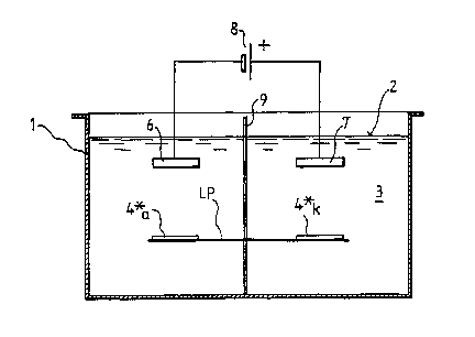
A bath container 1 is illustrated in Fig. 1 and is filled up to the level 2
with
a suitable treatment fluid 3. A circuit board- or conductive foil material
piece LP, for example a multi-layer laminate (multilayer) which is already
metallised and provided with conductive track structures 4 and with
borings, is guided through the treatment fluid 3 in a horizontal direction 5'
or 5" by means of suitable conveying means 3, such as for example rollers
or cylinders (not shown). In addition, there are two electrodes 6 and 7 in
the bath container which are connected to a current/voltage source 8.
The electrode 6 is cathodically polarised, the electrode 7 anodically
polarised. An insulation wall 9 (for example of plastic material) is
disposed between the two electrodes 6, 7 and screens the two electrodes
from each other electrically, transversely relative to the conveying
CA 02384249 2002-03-06
14
direction. This wall 9 is preferably introduced so tightly against the
material piece LP that said wall contacts or at least reaches up to said
material piece LP when passing by.
While the material piece LP is being moved past the electrodes 6, 7, it is
polarised, and indeed anodically in the regions 4*a, which are situated
opposite the cathodically polarised electrode 6, and cathodically in the
regions 4*~, which are situated opposite the anodic electrode 7.
If the material piece LP is guided past the electrodes 6, 7 for example in
the direction 5', then the structures 4 are etched. In this case, the left
region 4*a of the structure 4* is anodically polarised in the position shown
in Fig. 1 so that metal is etched away from the conductive track structure.
The right region 4*k of this structure 4* is, on the other hand, orientated
towards the anodically polarised electrode 7 and hence is negatively
polarised. If the treatment fluid 3 contains no further electrochemically
active redox pairs, hydrogen is generated in this region 4*k. In summary,
metal is therefore removed from the structures 4. This procedure
continues in the case of a singie structure 4 for as long as this structure is
situated simultaneously in the effective regions of both oppositely
polarised electrodes 6 and 7.
If the material piece LP is to be metallised, it must be transported in tie
direction S". In this case, a metallising bath is used as treatment fluid 3.
Firstly, the right edge of the material piece LP enters into the region of the
cathodically polarised electrode 6 and then into the region of the
anodically polarised electrode 7. The right part 4*k of the structure 4* is
situated opposite the anodically polarised electrode 7 in the position
shown in Fig. 1 and thus is polarised cathodically. On the other hand, the
left part 4*a of the structure 4* is situated opposite the cathodically
polarised electrode 6 so that this part is polarised anodically. If for
example a conductive track structure, which is made of copper as the
basic conductive layer, is to be treated with tin from an aqueons tinning
CA 02384249 2002-03-06
bath 3 which contains tin ions, then only oxygen is generated on the left
part 4*a of the structure 4*. On the other hand, tin is deposited on the
right part 4*k. To sum up, tin is thus deposited on the copper structures.
The same arrangement as described in Fig. 1 is shown in Fig. 2, provided
with a bath container 1 with electrolytic fluid 3. The level of fluid 3 is
designated by 2. In addition to Fig. 1, the effect of the electrical field of
the
electrodes 6, 7 on the material piece LP is reproduced schematically. An
insulation wall 9 is located between the electrodes 6 and 7. The metallic
structures 4*a and 4*k are connected together electrically. A more positive
potential is produced at the metallic structure 4*a, which is situated
opposite the cathodically polarised electrode 6 so that this region of the
structure is polarised anodically. A more negative potential is produced at
the structure 4*k by the oppositely situated anodically polarised electrode
7 so that this region is polarised cathodically. In the illustrated
arrangement, the structure 4*~ is metallised when the electrolytic fluid 3 is
a metallising bath. At the same time, an anodic process takes place at the
anodically polarised structure 4*a. If the electrolytic fluid 3 is a tin bath
and the structures are made of copper, copper is not dissolved. Instead of
this, oxygen is generated at the structure 4*a.
During the electrolytic process, both soluble and insoluble electrodes can
be used as electrodes. Soluble electrodes are normally used in the
metallising method so as to reform again by dissolution the metal used in
metallisation in the metallising solution. Thus, electrodes made of metal,
which is to be deposited, are used. Insoluble electrodes are also inert in
the treatment fluid during the current flow. For example, lead electrodes,
platinised titanium electrodes, titanium or noble metal electrodes coated
with iridium oxide can be used.
If the method and the device are used for electrolytic metallising, then a
metallising bath containing metal ions is used. When using soluble,
anodically polarised electrodes, the metal ions are supplied by dissolution
CA 02384249 2002-03-06
16
of these electrodes. On the other hand, if insoluble electrodes are used,
then the metal ions must be supplemented either by separate addition of
suitable chemicals or for example the device described in ~l0 9518251 A1
is used in which metal parts are dissolved by additional ions of a redox
pair, which ions are contained in the metallising bath. In this case, an
Fe2+/Fe3+ or another redox pair is contained in the copper baths.
In a further variant of the method and device, the electrodes can be
disposed in an electrode arrangement in such a way that they are
orientated on only one side of the material pieces. In order to avoid a
direct current flow in this case between the two electrodes, it is
advantageous to dispose at least one insulation wall (for instance made of
a polyimide film which is 50 ~m thick) between the electrodes and to move
said wall very near to the material pieces. The insulation walls are
preferably disposed in such a way that they contact the material pieces
when being transported through the electrolytic bath or that they reach at
least directly up to the surfaces of the material pieces. As a result, an
especially good screening of the anodic electrode from the catholic
electrode is achieved.
Since small structures to be metallised must be situated opposite both at
least one catholic and at least one anodic electrode for electrolytic
treatment, the spacing between the electrodes, given an established size of
the structures, must not exceed a specific value. Consequently, a top limit
is also established for the thickness of the insulation wall. As a rule of
thumb, it can be assumed that the thickness of the insulation wall should
correspond at most to approximately half of the extension of the
structures to be metallised, preferably comparing the dimensions
respectively in the conveying direction of the material. In the case of
structures with a width of approximately 100 hum, the thickness of the
insulation wall should not exceed 50 Vim. In the case of narrower
structures, correspondingly thin insulation walls should be used.
17
Further insulation walls can be provided in addition between the
individual electrode arrangements in order to avoid a direct current flow
between the electrodes of further electrode arrangements which are
disposed one behind the other.
In an alternative method and device variant, the electrodes of an electrode
arrangement can also be disposed in such a way that they are orientated
on different sides of the material pieces. In this case, the material pieces
themselves function as insulation walls between the electrodes so that the
use of other insulation walls between the electrodes of an electrode
arrangement can be dispensed with when the electrodes do not protrude
beyond the material pieces. This method and device variant can be
applied when the electrically conductive regions on both sides of the
material pieces are connected to each other electrically. This arrangement
is suitable for example for the treatment of through hole plated circuit
boards and conductive foils which are functional on one side. As a result
of the fact that for example material pieces with a whole-surface
electrically conductive layer are used on the side situated opposite the
functional side, the cathodically polarised electrode can be disposed
opposite this conductive layer and the anodically polarised electrode
opposite the functional side, in order to deposit metal on the conductive
structures of the functional side. At the same time, metal is removed from
the oppositely situated conductive layer.
When implementing the method according to the invention, care must be
taken that a direct current flow cannot flow between the cathodically
polarised electrodes and the anodically polarised electrodes of an electrode
arrangement. For this purpose, either the above-mentioned insulation
walls or the material pieces themselves can be used if the oppositely
polarised electrodes of an electrode arrangement are orientated on
different sides of the material pieces. A third possibility for avoiding a
direct current flow e.~ists when the material pieces are not plunged in the
treatment fluid but are brought in contact with the fluid by means of
CA 02384249 2002-03-06
18
suitable nozzles. In this case, the insulation walls between the electrodes
of an electrode arrangement, which electrodes are orientated on one side
of the material pieces, can be totally dispensed with, when the fluid
regions, which are in contact with the individual electrodes, are not in
contact with each other.
An electrode arrangement can extend perpendicularly or diagonally to the
direction in which the material pieces are transported in the treatment
unit, preferably over the entire treatment width of the conveying plane.
The spatial extension of the electrode arrangements, observed in conveying
direction, has a significant effect on the duration of the electrolytic
treatment. Long electrode arrangements can be used for whole-surface
treatment. On the other hand, very short electrode arrangements must be
used when treating very fine structures.
This can be explained in more detail with reference to Fig. 1. If the
material pieces LP are moved from left to right (conveying direction 5";
case: electroplating), the leading right edge of a structure 4* is
electroplated longer than the rear regions of the structure. As a result, an
irregular layer thickness is obtained. The maximum thickness of the layer
depends substantially upon the length of the electrode arrangement in the
conveying direction 5', 5" and, furthermore, upon the conveying rate, the
current density and the dimensions of the structures 4 in conveying
direction 5', 5". Long electrode arrangements and, at the same time, long
structures 4 in conveying direction 5', 5" result, measured absolutely, in
large differences in layer thickness in the case of a large initial layer
thickness. When the electrode arrangements have a smaller length in
conveying direction 5', 5", the differences in layer thickness become
smaller. At the same time, the treatment time is reduced. The
dimensions of the electrode arrangements can therefore be adapted to
requirement. In the case of the finest conductive track structures, for
example 0.1 mm pads or conductive tracks of 50 ~m width, the length of
the electrode arrangements should be in the sub-millimetre region.
CA 02384249 2002-03-06
19
In order to multiply the effect of the method, at least two electrode
arrangements can be provided in one treatment unit and the material
pieces can be guided past said electrode arrangements successively. The
electrodes of these electrode arrangements can have an extended
configuration and be disposed substantially parallel to the conveying
plane. The electrodes can be orientated either substantially perpendicular
to the conveying direction or to form an angle a ~ 90° to the conveying
direction. Said electrodes extend preferably over the entire width of the
conveying plane covered by the material pieces.
With an arrangement in which the electrodes form an angle a ~ 90°
to the
conveying direction, it is achieved that electrically insulated metal
structures, which are orientated both parallel to the conveying direction
and perpendicular thereto, are subjected longer to the desired electrolytic
reaction than when a ~ 90° (~ 25°). If the angle were a ~
90°, then the
conductive tracks, orientated in the conveying direction and at a given
conveying rate and given electrode length, would be electrolytically treated
for an adequate length of time, while conductive tracks orientated
perpendicular thereto would only be treated in the electrode arrangement
for a short period of time. This is due to the fact that electrolytic
treatment is only possible if the structure is situated at the same time
opposite the anodically polarised and the cathodically polarised electrode
of an electrode arrangement. In the case of structures, which are
orientated parallel to the electrode arrangement and hence to the
electrodes, this contact time is short. The reverse applies when the
electrode arrangements are orientated parallel to the conveying direction
(a ~ 0° (~ 25°))~
The device according to the invention can also have a plurality of electrode
arrangements with electrodes in an extended configuration, the electrodes
of the different electrode arrangements forming different angles to the
conveying direction. In particular, an arrangement of at least two
CA 02384249 2002-03-06
20
extended electrode arrangements is advantageous, the angle between the
electrode arrangements and the conveying direction of the material pieces
in the treatment unit being a ~ 90° and the electrode arrangements
being
disposed approximately perpendicularly to each other. Preferably, al ~
45°
(first electrode arrangement), especially 20° to 70°, and a2 ~
135° (second
electrode arrangement), especially 110° to 160°.
In an especially preferred method, the electrodes are moved in an
oscillating manner substantially parallel to the conveying plane.
Furthermore, there can also be provided a plurality of electrode
arrangements, which are disposed parallel to each other and adjacent and
have electrodes in an extended configuration and insulation walls
disposed respectively between said electrodes, and adjacent electrodes can
be supplied respectively from a separate current/voltage source. In this
case when for example a metallising solution is used, metal is firstly
deposited on the insulated structures of the material pieces. Since the
regions of the structures which are at the front during transportation are
situated for longer in the metallising region than the rear structures, the
thickness of the metal layer on the former is greater. If the material pieces
then pass the second electrode arrangement, which comprises the second
electrode in the first arrangement or a third electrode and a further
oppositely polarised electrode in the second arrangement, then a lot of
metal is removed again from the front regions of the material pieces and,
on the rear structures, more metal is deposited than removed. Hence to
sum up, an averaging of the thickness of the metal layer on the structures
is effected during treatment in the two electrode arrangements.
In order to achieve an especially uniform metal layer thickness with this
arrangement, the current density on the structures situated opposite the
first electrode arrangement can be adjusted to a value which is
approximately twice as great as the current density on the structures
situated opposite the second electrode arrangement.
CA 02384249 2002-03-06
' CA 02384249 2002-03-06
21
In a further preferred method, after being guided past at least one
electrode arrangement, the material pieces can also be rotated by 180°
about an axis which is perpendicular to the conveying plane and be
delivered to the same or to a further electrode arrangement. As a result, a
more uniform layer thickness distribution is effected during electrolytic
treatment of structures which are orientated in any manner.
In a further preferred method, the electrode arrangements can in addition
be surrounded by insulation walls. If a plurality of adjacent electrode
arrangements is used, these insulation walls are disposed between the
electrode arrangements. Openings, which are orientated town rr1 ~ r~, P
conveying plane, are formed through these insulation walls, which
surround the electrode arrangements, and through the insulation walls,
which are disposed between the electrodes.
These openings can have widths of various sizes in accordance with the
existing requirements. For example, these openings have, regarded in the
conveying direction, such a width respectively that the openings
associated with the cathodically polarised electrodes are smaller than the
openings associated with the anodically polarised electrodes when the
method for depositing metal on the material pieces is used, or that the
openings associated with the cathodically polarised electrodes are greater
than the openings associated with the anodically polarised electrodes
when the method for etching metal surfaces on the material pieces is
applied.
It is achieved with this embodiment that the current density at the
regions, situated opposite the cathodically polarised electrodes, on the
material pieces to be treated is different from the current density at the
regions which are situated opposite the anodically polarised electrodes.
Due to these differences, potentials of different magnitude can be set at
these regions to favour specific electrolytic processes and to repress
others. Hence, it is possible for example to speed up the deposition of
22
metal relative to the competing dissolution of the metal in order also to
deposit metals at a greater thickness on the material pieces in this
manner. Because in the above-mentioned case the current density, and
hence the potential, at the region on the material pieces, which is situated
opposite the cathodically polarised electrode, is increased, there occurs
there as a competing reaction, the decomposition of water (generation of
oxygen). As a result, Iess metal is dissolved than is deposited at the
material surfaces which correspond to the anodically polarised electrodes.
The reverse is of course true for an application in which metal is etched.
In order to prevent metal deposition on the cathodically polarised
electrodes, these can be screened with ion-sensitive membranes so that
electrolytic spaces are formed which surround the cathodically polarised
electrodes. If ion-sensitive membranes are not used, deposited metal on
the cathodically polarised electrodes must be removed again on a daily or
weekly basis. For this purpose, for example a cathodically polarised
surface electrode can be disposed for stripping these electrodes, the
metallised electrodes being anodically polarised in this case. These
stripping electrodes can be introduced into the electrode arrangement
during production breaks instead of the material pieces to be treated. A
cyclical exchange is also very simple with external stripping of the
cathodically polarised electrodes.
Furthermore, it can be advantageous for treating the material pieces to
modulate the electrical voltage applied to the electrodes of the electrode
arrangements in such a way that a unipolar or bipolar current pulse
sequence flows to the electrodes.
The subsequent Figures serve to further explain the invention and show in
detail:
Fig. 3: a schematic illustration of the construction of an electrode
arrangement;
CA 02384249 2002-03-06
23
Fig.4: the layer thickness configuration of a structure after
treatment in the device according to Fig. 3;
Fig. 5: a schematic illustration of two electrodes of an electrode
arrangement;
Fig. 6: a schematic illustration of a plurality of electrodes which are
associated with various electrode arrangements;
Fig. 7: a special arrangement of a plurality of electrode arrangements
along a conveying route for the material pieces in a
continuous system;
Fig.8a: a section through a continuous system with a vertical
conveying plane;
Fig. 8b: a plan view of a continuous system with a vertical conveying
plane;
Fig. 9: a lateral section through a continuous system in which the
material pieces are transported in a horizontal conveying
plane;
Fig. 10: a schematic illustration of a seal film in front elevation;
Fig. 11: a plan view of a material piece with copper structures and a
projection of the electrodes from a plurality of electrode
arrangements;
Fig. I2: a further special arrangement of a plurality of electrode
arrangements along the conveying route for the material
pieces in a continuous system.
An electrode arrangement according to Figs. 1 and 2 is eminently suitable
for treating large-surface metal surfaces. The length of the electrodes in
conveying direction determines, together with the conveying rate, the
duration of the electrolytic treatment with an electrode arrangement. In
the case of large surfaces or lar;e structures to be treated, a large
electrode length in conveying direction is chosen, at least if this concerns
the process-determining electrode.
CA 02384249 2002-03-06
CA 02384249 2002-03-06
24
If care is taken by means of appropriate process parameters that the
treatment effect achieved firstly at the first electrode is not reversed again
or at least not entirely by treatment at the second electrode of an electrode
arrangement, then a plurality of electrode arrangements according to the
invention can be disposed successively in conveying direction, i.e. a
material piece is guided past a plurality of electrode arrangements
successively. The respective treatment results, which are achieved with
the individual electrode arrangements, accumulate. The length of the
electrode arrangements in conveying direction must be adapted to the size
of the structures to be treated. When treating small structures, this
length must also be selected to be small. The number of electrode
arrangements must be chosen to be correspondingly greater when a
treatment outcome is required. It is always a prerequisite that the
treatment outcome is not reversed again by the respectively subsequent
electrode of an electrode arrangement. For example, an already deposited
metal layer should not be removed again when passing a subsequent
cathodically polarised electrode.
In the case of very small structures to be treated, the treatment of the edge
regions of structures to be treated, which are guided past the electrodes
firstly or lastly, comes to the fore. However, these edge regions should
also be electrolytically treated in as uniform a manner as possible. For
this purpose, the possibility of being able to set electrochemically
"oppositely directed" reactions (for example metallising, stripping) in the
electrode arrangement in a targeted manner is used advantageously. With
reference to Fig. 3, the very uniform electrolytic treatment of even the
smallest structures (width 0.1 mm) is described.
In Fig. 3, an arrangement with two electrode arrangements is reproduced
which have respectively anodically and cathodically polarised electrodes
6', 7', 6", 7". A material piece LP with the structures 4, for example
conductive track structures made of copper, is guided in conveying
' CA 02384249 2002-03-06
direction 5 through a not-shown electrolytic fluid. A tin bath is used in
this example as electrolytic fluid.
The cathodically polarised electrodes 6', 6" are screened by ion-sensitive
diaphragms 16 from the surrounding electrolytic space. As a result, the
deposition of tin on the electrodes 6', 6" from the electrolytic fluid is
prevented. Insulation walls 9' or 9" are located respectively between the
electrodes 6' and 7' or 6" and 7". An insulation wall 17 is disposed
between the two electrode arrangements. The diaphragms 16 can also be
dispensed with. In this case, the cathodically polarised electrodes need to
be stripped from time to time.
The structures 4 are metallised in the first electrode arrangement in which
the electrodes 6' and T are located. As a result of the fact that the
structures 4 are guided past the electrode arrangement from left to right,
the right edge of the structures 4 is subjected for a longer time to the
electrolytic reaction than the left edge so that the deposited quantity of
metal and hence the thickness of the metal layer is greater than on the left
edge. In order to compensate at least in part for this lack of balance, the
material piece LP is guided past the second electrode arrangement after
passing through the first electrode arrangement. In this arrangement, the
sequence of the cathodically polarised electrode 6" and of the anodically
polarised electrode 7" is changed relative to the polarity of the electrodes
6'
and 7' in the first electrode arrangement so that the left edge of the
structures 4 respectively is subjected for a longer time to the
electrochemical (electroplating) effect of the electrode 7" than the
respective right edge. The right edge of the structures 4 is anodically
polarised when passing the cathodically polarised electrode 6" and hence
is subjected for a longer time to the anodic reaction than the left edge of
the structures 4 so that, in this case, metal is preferably removed again on
the right edge. As a result, a substantially uniformly thin layer of tin is
deposited.
26
This result can be understood with the help of the diagram in Fig. 4 in
which the obtained metal layer thickness d is reproduced as a function of
the length extension a of the structure 4 to be coated. This diagram was
drawn up with the condition that the current in the second electrode
arrangement is half as great as in the first electrode arrangement and that
the current yield of the electrochemical reactions (metal dissolution, metal
deposition) is close to 100%.
The layer thickness distribution, which can be measured after the material
piece has passed through the first electrode arrangement, is designated by
the curve I. On the left edge of the structures 4 (a = 0), practically no
metal has been deposited, while on the right edge (a = A) the layer
thickness D is achieved. Two processes take place when passing the
second electrode arrangement: at the left edge, in practice only metal is
deposited (partial process, displayed by curve II). Thus, the layer
thickness D/2 is achieved in this region. In addition, in practice only
metal is removed at the right edge (partial process, displayed by curve III).
Thus, the layer thickness at this location is reduced from originally d = D
to d = D/2. The intermediate regions on the structure likewise have
substantially a layer thickness of d = D / 2. The resulting layer thickness
distribution is indicated in curve IV.
By optimising the treatment bath, the metallisation can be improved even
further: by using a bath for metal deposition, which does not permit metal
dissolution, a greater metal layer thickness can be achieved in total. In
this case, the currents of the first and of the second electrode arrangement
must be of equal size. The curve III shown in Fig. 4 coincides in this case
with the abscissa since no metal is dissolved. Therefore, a thickness D of
the layer is obtained which is constant over the total surface of the metal
structures (curve IV').
A further simplification of the arrangement according to Fig. 3 is achieved
in that the central regions with the electrodes 7', 7" are combined so as to
form one region with one electrode. In this case, two current/voltage
CA 02384249 2002-03-06
z .
27
sources are also required to supply current to the electrodes with which
the different currents to both partial electrode arrangements, comprising
the electrode 6' and the electrode 7', 7", on tl'~e one hand, and the
electrode 7', 7" and the electrode 6", on the other hand, can be produced.
The dividing wall 17 is dropped in this case. The mechanical assembly of
the electrode arrangements is particularly simple in this case.
The schematic assembly of the electrode arrangement in a preferred
embodiment of the invention is reproduced in Fig. 5. The material piece
LP with the structures 4 is illustrated underneath the electrode
arrangement (the structures 4 situated on the underside of the material
piece LP are electrolytically treated by a second electrode arrangement on
the underside of the material piece). The material piece LP is guided in the
conveying direction 5. The electrode arrangement comprises electrodes 6
(cathodic) and 7 (anodic). Between the electrodes 6 and 7 there is an
insulation wall 9 which is situated in this case on the material piece LP
and effects an effective, electrical screening of the field lines which
emanate from the electrodes 6 and 7. The electrodes 6 and 7 are
surrounded by the cathodic space 10 and the anodic space 11 in which
the electrolytic fluid 3 is located. Both spaces 10 and 11 open towards the
conveying plane in which the material piece LP is guided. Focussing of the
effect of the electrodes on a small region of the material piece LP is
achieved by two small openings 12~ and 12a which are formed through the
lateral insulation walls I3, 14 and the insulation wall 9 between th.e
electrodes 6 and 7. This is advantageous since, as a result, the electrolytic
treatment of the small structures 4 is evened out. In contrast thereto, the
electrolytic treatment of small structures, when large openings 12a and
12k are chosen, is irregular.
As can also be detected in Fig. 5, the electrolytic fluid 3 is fed into the
electrode arrangements from above (shown by the arrows 15). The
electrochemical reaction can be speeded up because of the high flow rate.
CA 02384249 2002-03-06
' 28
In Fig. 6 there is shown a further arrangement according to the invention
with a plurality of adjacent electrodes 6, T, 7". The electrodes 6, 7', ?" are
connected to the current/voltage sources 8', 8", for example galvano-
rectifiers. Insulation walls 9 are located between the electrodes. A
material piece LP to be treated is moved in conveying direction 5 in the
conveying plane. The respective electrolytic spaces, which surround the
electrodes 6, 7, have openings I2a, 12k, which are orientated towards the
conveying plane and are formed by the insulation walls 9. These openings
12a, I2k are of different sizes. As a result, current densities of different
size are set and hence also different potentials at the regions 4, 4* on the
material piece LP which are situated opposite the openings 12a, 12~.
In the situation where a material piece LP provided with metallic regions 4
is treated in a metal deposition solution, the following situation arises.
As a result of the fact that the opening 12k on the cathodically polarised
electrode 6 is smaller than the opening 12a, on the anodically polarised
electrode 7, a higher current density and hence a higher potential is set at
the regions 4*a situated opposite the cathodically polarised electrode 6
than is set at the regions 4*k of the treated region 4*, which regions are
situated opposite the anodically polarised electrodes T, 7". Consequently,
the competing oxygen generation will take place also, in addition to metal
dissolution, during the anodic partial process in the region of the
cathodically polarised electrode 6 so that less metal is removed in this
region 4*a than the amount of metal deposited in the region 4*k. In
summary, a metal layer is thus formed.
In Fig. 7, a special arrangement of a plurality of electrode arrangements
18 along the conveying route for the material pieces zn a continuous
system is reproduced in plan view. The electrodes in the arrangement of
Fig. 1 are schematically illustrated by the continuous and broken straight
lines. The electrode arrangements 18 are set slightly diagonally in the
conveying direction 5 and extend at a corresponding length in the
CA 02384249 2002-03-06
p i
29
electrolytic unit. Each electrode arrangement 18 serves only for treating a
part of the surface of the material pieces to be treated. Hence, the
treatment time is significantly increased. If the electrolytic unit has for
example a length of 1.40 m and a width of 0.2 m, then, in the illustrated
arrangement with four electrode arrangements 18, there results an
increase in treatment time of 1400 mm x 4/200 mm = 28. In the case of
an active length of an electrode arrangement 18 of 1 mm, there results
hence a treatment time of approximately 17 sec, at a conveying rate of for
example 0.1 m/min. With an average deposition current density at the
level of 10 A/ dm2, the layer thickness of deposited copper is approximately
0.6 Vim. If a plurality of electrodes is used to treat partial regions of the
material pieces, then the layer thickness multiplies with the number of
electrodes.
A continnous system 1 is illustrated in section in Fig. 8a. The material
pieces LP are transported in this case by a gripping mechanism 19, for
example a clamp or by cylinders which are not shown here, and held
vertically. The material pieces LP are introduced into a container 1 from
the side, said container containing the treatment bath, for example a
metallisation solution 3. This solution is continuously withdrawn from
the container by means of a pump 21 via suitable pipelines 20 and guided
over a filter 22 before said solution is fed back into the container 1. In
addition, air can be introduced via a pipeline 23 in the container 1 ~in
order to add turbulence to the solution 3.
In Fig. 8b, the unit shown in Fig. 8a is reproduced in a plan view, the
fittings only being illustrated in part. The material pieces LP are guided in
conveying direction 5. The treatment fluid 3 is situated internally of the
container 1, in this case a solution which is suitable for electrolytic
etching. The material pieces LP are introduced via the opening 24 and
through squeeze rollers 25 into the container and between squeeze rollers
26 and through the opening 27 once again out of the container.
CA 02384249 2002-03-06
30
In the container 1, there is a plurality of electrode arrangements, which
are disposed successively and on both sides of the conveying plane for the
material pieces LP, said electrode arrangements being formed respectively
from cathodically polarised electrodes 6', 6", 6"', ... and anodically
polarised electrodes 7', ?", 7"', .... Insulation walls 9 are situated between
the electrodes. These insulation walls 9 have elastic seal films 31 which
make possible complete screening of the electrical fields of the individual
electrode spaces from each other in that they contact the material surfaces
when passing the material pieces LP. The electrodes 6', 6", 6"', ..., T, ?",
7"', ... are connected to a galvano-rectifier 8, the connections of the
electrodes shown on the right in Fig. 8b to the rectifier not being
illustrated. Each electrode arrangement can also be supplied from
separate rectifiers.
When the material pieces LP are guided for example first past an
anodically polarised electrode and then past a cathadically polarised
electrode, metal is electrolytically removed.
In Fig. 9, a horizontal unit (continuous system with a horizontal conveying
plane) is illustrated in lateral section. The container 1 contains the
treatment fluid 3. The material pieces LP to be treated are guided in the
treatment fluid 3 past the electrode arrangements in a horizontal
conveying direction 5. The electrode arrangements in turn comprise
respectively cathodically polarised electrodes 6', 6", 6"', ... and anodically
polarised electrodes 7', 7", 7"', ... The electrode arrangements are
disposed on both sides of the conveying plane in which the material pieces
LP are guided.
In the present case, insulation rollers 28 with sealing lips are used to
insulate the electrodes 6', 6", 6"', ..., 7', 7", 7"', ... from each other.
Instead of insulation rollers 28, insulation walls 9 with seal films 31 can
also be used.
CA 02384249 2002-03-06
31
In the right part of Fig. 9, an alternative embodiment and arrangement of
the electrodes 6"', 7"' relative to the insulation walls 9 and seal films 31
is
illustrated.
In Fig. 10, a detail of an insulation between the electrodes of an electrode
arrangement is illustrated in front elevation. In order to achieve a secure
seal during treatment of thicker circuit boards LP, the seal film 31 can be
spring-loaded on the insulation wall. Gaps are thus avoided which can
arise laterally to the passing circuit board LP.
Fig. 11 shows a plan view of a structured material piece, which is
conveyed in a continnous system, for example a circuit board laminate LP
which has metal sacrificial regions 29 and regions 30 provided with metal
structures (structures not shown) which are connected to each other
electrically. This material piece LP can be treated for example in a
horizontal unit by being brought in contact with the treatment fluid and
being guided past the electrode arrangements according to the invention.
The electrodes 6, 7 of the electrode arrangements are illustrated here in
projection on the material piece LP. The anodically polarised electrodes 7
are orientated on the structured regions 30 and designated by "~" and the
cathodically polarised electrodes 6 are orientated on the sacrificial regions
29, which are made of metal and are designated by "8". Insulation walls 9
are disposed between the electrodes 6 and 7. The insulation walls 9 and
the electrodes 6, 7 are only indicated in the illustration of Fig. 11, this
detail concerning a section representation through the plane of projection
of the Figure 11.
The material piece is guided in one of the conveying directions S' and 5".
The sacrificial regions 29, which are made of metal, are continuously
guided past the cathodically polarised electrodes 6 and thus are dissolved.
The structured regions 30, on the other hand, are metallised since they
are guided past the anodically polarised electrodes ?. By means of this
CA 02384249 2002-03-06
32
arrangement, it is possible for a metal to be deposited which is identical to
the metal from which the structured regions 30 are made.
A further preferred device according to the invention is illustrated
schematically in Fig. 12. The material pieces are guided past the electrode
arrangements in conveying direction 5, said electrode arrangements
comprising respectively extended electrodes 6', 6", 6"', ... and 7', 7", 7"',
...
The electrode arrangements with the electrodes form an angle al or an
angle a2 relative to the conveying direction 5. As a result, the effect of the
treatment time of structures which are orientated differently relative to the
conveying direction 5 is compensated for. Since, in the case of circuit
boards, the conductive tracks usually extend parallel or perpendicular to a
lateral edge of the boards and hence parallel or perpendicular to the
conveying direction 5, a treatment time of equal length is achieved for
conductive tracks of both orientations by means of the illustrated
orientation of the electrode arrangements, as long as these conductive
tracks of both orientations have the same length.
CA 02384249 2002-03-06
' ~ 33
Reference symbols:
1 bath container
2 level of the treatment fluid 3
3 treatment fluid
4 metallic structure/ surface on the material pieces
LP
4* treated metallic structure 4
4*a anodically treated metallic structure 4
4*k cathodically treated metallic structure 4
5, 5', 5" conveying direction
6, 6', 6", cathodically polarised electrodes
6"'
7, 7', 7", anodically polarised electrodes
7"'
8, 8', 8" current/voltage sources
insulation wall
cathodic space
I 1 anodic space
12 opening of the electrode arrangement to the bath
container
I2k opening to the cathodically polarised electrode
12a opening to the anodically polarised electrode
13 insulating lateral wall of the electrode arrangement
14 insulating lateral wall of the electrode arrangement
I5 flow direction of the treatment fluid 3
16 diaphragm
17 insulation wall between two electrode arrangements
18 electrode arrangement
19 clamp
electrolytic line
21 pump
22 filter
23 air supply
24 inlet opening
squeeze roller
CA 02384249 2002-03-06
34
26 squeeze roller
27 outlet opening
28 insulation roller
29 sacrificial region
30 structured region
31 seal film
LP sheet/foil material piece
CA 02384249 2002-03-06