Note: Descriptions are shown in the official language in which they were submitted.
CA 02384608 2002-02-06
WO 01/16991 PCTIUSOO/20905
ELECTRON BEAM APPARATUS HAVING A LOW LOSS BEAM PATH
FIELD OF THE INVENTION
The present invention is directed to a method and apparatus for electron beam
irradiation of a single layer or multi-layer article, and resulting products.
More
particularly, the invention is directed to use of a low loss electron beam
path to
irradiate an electron beam modifiable material coated on an electron beam
degradable
substrate.
BACKGROUND
In recent years, electron beam radiation has increasingly been used for
modifying various materials, including polymerizing, crosslinking, grafting,
and
curing materials. For example, electron beam processing has been used to
polymerize
and/or crosslink various pressure-sensitive adhesive formulations coated on
film
substrates, to graft coatings onto substrates, and to cure various liquid
coatings, such
as printing inks. Using an electron beam to modify a material avoids the need
for
coating solutions, including those comprising volatile organic compounds
("VOCs").
This allows for a reduction in VOC emissions, and a concurrent reduction in
energy
costs and environmental or occupational hazards.
Unlike ultraviolet ("UV") radiation, which is also used to crosslink,
polymerize, graft, and cure various materials, electron beam radiation does
not require
the use of an initiator. In addition, electron beam radiation is readily
absorbed by all
organic materials, even those materials that are not readily modified by UV
radiation,
such as thick, opaque materials and those that resist UV modification, such as
allylic,
olefinic, and unsaturated compounds. Polyethylene is an exemplary unsaturated
compound that cannot readily be cured by UV radiation, but is curable by
electron
beam radiation.
CA 02384608 2002-02-06
WO 01/16991 PCTIUSOO/20905
Although electron beam radiation has many advantages, it does have some
limitations. These limitations include the fact that electron beam generating
equipment has traditionally been relatively expensive. The high expense is at
least
partially associated with the need for large power supplies, lead shielding,
high
voltage components, and safety monitoring equipment. In recent years,
manufacturers
have been able to build less expensive, more compact, lighter electron beam
equipment by lowering the voltage of the electron beam to 125 kilovolts (kV)
or less.
For example, Energy Sciences, Inc. of Wilmington, Massachusetts; Advanced
Electron Beam Technologies, Wilmington, Massachusetts; and American
International Technologies, Inc. of Torrance, California are manufacturers of
compact,
low cost electron beam generators. These machines make it possible to lower
the
purchase and operating costs of electron beam radiation equipment.
Another significant limitation of electron beam radiation is that electrons
frequently penetrate too deeply into the material being irradiated. High
voltages are
frequently used to obtain a reasonably uniform dose over the entire cross-
section of an
electron beam modifiable coating, but this can result in a significant amount
of
energetic electrons passing into layers below the electron beam modifiable
coating.
This becomes a problem in multi-layer materials that comprise a coating of
material
that is being modified, and a substrate or backing of material that can be
damaged by
electron beam radiation. Paper, polyvinyl chloride, polypropylene, and TEFLON
are
all materials that often are used as substrates for adhesives, yet are
susceptible to
degradation from electron beam radiation. Electron beam radiation can cause
the
substrate to become brittle or otherwise degraded. The result is a
deteriorated
substrate that makes the product either lower quality or unusable for its
desired
application.
SUMMARY OF THE INVENTION
Existing electron beam generation systems do not adequately address the
problems of high machine costs and satisfactorily modifying a coating without
degrading the substrate. Consequently, a need exists to control electron beam
irradiation such that the electron beam penetration is substantially limited
to specific
layers of the irradiated material, preferably just the electron beam
modifiable coating
of the material.
2
CA 02384608 2002-02-06
WO 01/16991 PCTIUSOO/20905
The present invention is directed to an apparatus and method for delivering
electron beam radiation to a material, particularly a multi-layer material
having an
electron beam modifiable coating and an electron beam degradable substrate.
The
invention is also directed to products manufactured using the apparatus and
method of
the invention. At least one embodiment of the present invention allows one to
control
the dose (energy deposited per unit mass) delivered to particular depths in an
irradiated material.
One aspect of the invention is directed to an electron beam apparatus
comprising an electron beam source, a window proximate the electron beam
source
comprising a polymeric film having at least two surfaces, a protective layer
resistant
to free radical degradation on at least one surface of the polymeric window, a
support
proximate the window on which to place materials to be irradiated by the
source, and
a gap between the window and support.
Another aspect of the invention is directed to a window for use with an
electron beam source comprising a polymeric film having at least two surfaces,
the
film having a protective layer resistant to free radical degradation on at
least one
surface wherein the film is able to contain an environment having a pressure
of less
than 10 -4 Torr.
Another aspect of the invention is directed to a method of irradiating an
article with an
electron beam comprising providing an electron beam source; providing a window
for
use with the electron beam source, the window comprising a polymeric film
having at
least two surfaces a protective layer resistant to free radical degradation on
at least one
surface; and irradiating the article through the window with electrons from
the
electron beam source.
Another aspect of the invention is directed to a method of modifying the
properties of an article having two or more layers comprising providing an
article
having an electron beam modifiable first layer and an electron beam degradable
second layer proximate the first layer; providing an electron beam source for
which
energy, voltage, and current levels may be adjusted; providing a window
between the
electron beam source and the article to be irradiated, wherein a gap exists
between the
window and article, the window having a unit path length of 3 to 50 grams per
square
meter, setting the electron beam source energy to between 50 and 150 keV;
adjusting
the electron beam source voltage and current, and adjusting the gap distance
between
3
CA 02384608 2002-04-29
60557-6654
the window and article such that the electron beam can modify the first layer
without
substantially degrading the second layer, and irradiating the article with an
electron
beam from the electron beam source.
Another aspect of the invention provides an electron beam modified article
comprising an electron beam degradable backing material, and an electron beam
modified coating on the backing material, the 30 micrometers of the
electron=beam
degradable backing adjacent the modified coating having absorbed between 0 . 1
and 4 0
mJ/cm2 of energy.
Another aspect of the invention provides an electron beam modified article
comprising an electron beam degradable backing material, and an electron beam
modified coating on the backing material, the modified coating being free of
release
material contamination. Because the present invention allows an electron beam
modifiable layer to be modified, e.g., cured, directly on an electron beam
degradable
backing without materially degrading the backing, the modifiable layer is not
required
to be modified on a release material, such as silicone, then transferred to
the backing.
This eliminated the possibility of the modifiable layer being contaminated
with release
material.
In in-adiating an electron beam modifiable material coated on an electron beam
degradable substrate, it is important to provide a dose to, and through, the
irradiated
material that will adequately modify the modifiable layer so it will be useful
for its
intended purpose and so it will adhere to the substrate. However, it is
important that
the dose is not excessive. For example, when an adhesive layer on a substrate
is
irradiated, the surface dose must be sufficient to impart important adhesive
properties
such as cohesive and adhesive strength, but the dose should not be 'so high
that it over-
modifies, e.g., over-crosslinks, or degrades the adhesive layer (which would
limit its
adhesive properties). The dose must also be sufficient to modify the adhesive
at the
adhesivelsubstrate interface so the adhesive will bond with the substrate.
However,
the interface dose should not be so high that the substrate is significantly
degraded.
The electron beam apparatus of the present invention includes an electron
beam source configured and arranged to direct electrons into a material, most
suitably
a multi-layer material having both an electron beam modifiable upper layer and
a
electron beam degradable lower layer. In traveling from the electron beam
source, the
electrons pass from a vacuum environment through a window foil having low
electron
4
CA 02384608 2002-02-06
WO 01/16991 PCTIUSOO/20905
absorbency properties (a "low loss" window) into an atmospheric pressure
environment containing the material to be irradiated. The route of the
electron beam
from its source, through the low loss window, to the irradiated material is
sometimes
referred to herein as the low loss path. By using a low absorbency window,
even a
relatively low voltage electron beam can pass through the window with only a
slight
reduction in power. The resulting electron beam is able to enter and modify
the
coating of the irradiated material, preferably without entering and degrading
any
substrate.
Appropriate window materials for use in the low loss path include polymeric
films, such as polyimide films. A protective layer is placed on at least the
window
surface facing the atmospheric pressure environment to reduce free radical
degradation and thus improve performance and durability. The protective layer
may
be a thin layer of aluminum or other metal that protects against free-radical
degradation. Preferably it also enhances electrical and thermal conduction
along the
film.
After the electrons pass through the window, they travel through a gap
between the window and the material being irradiated. The gap normally
contains
nitrogen gas or another inert material maintained at approximately atmospheric
pressure. The gap distance is preferably minimized to increase the dosage of
electron
beam radiation delivered to the modifiable coating and to reduce the dosage
absorbed
by electrons in the gap. Reducing the gap distance also improves the energy
efficiency of the apparatus such that lower voltages may be used to irradiate
a
material. The gap between the window and the irradiated material is between
about 2
and 100 millimeters in certain embodiments, between 4 and 50 millimeters in
other
embodiments, and between about 5 and 20 millimeters in yet other embodiments.
The
preferable gap size will depend on factors such as the window material, the
presence
of a window clamp structure, the voltage used, and the thickness of the
modifiable
layer.
The amount of electron energy absorbed by the window, gap, coating layer,
and any substrate layer as the electron beam travels through these regions can
be
determined and plotted on a depth/dose curve, which plots dose absorbed
against
distance from the electron beam source. The dimensions of the curve may vary
depending on numerous conditions, but it will typically have a peak where
energy
5
CA 02384608 2002-02-06
WO 01/16991 PCTIUSOO/20905
absorption is the greatest. In conventional electron beam systems, this peak
often
exists in the window or gap region. The ideal depth/ dose curve would have a
square
wave shape such that the window and gap absorbed no energy, the modifiable
material
layer absorbs a uniform amount of energy through its total depth and the
degradable
substrate absorbed no energy.
A principle advantage of the low loss beam path is that it can shift the
absorption peak, also referred to in the art as "back scatter" peak, of the
depth/dose
curve out of the window/gap region and into the coating layer region such that
the
depth/dose curve better approximates the ideal square wave curve. At the same
time,
the lower voltage permitted by the low loss beam path characteristically
produces a
depth/dose curve having a steep negative slope over the remaining depth of
penetration subsequent to the absorption peak. Accordingly, appropriate
selection of
window materials and gap distances allows the generation of a depth/dose curve
having a declining slope that may closely coincide with the interface between
the
substrate and the coating.
Per the present invention, the electron beam radiation dosage may rapidly
diminish upon entry into the irradiated material such that the dose received
by a
coating may be significantly more than that received by a substrate. The
proportion of
the total dose received by the substrate is affected by factors such as the
shape of the
depth/dose curve, the window material, the gap distance, the voltage required
to
achieve satisfactory modification of the coating, and the thickness of the
substrate. In
some embodiments the dose may be 1 to 5 times greater at the coating surface
than at
the coating/substrate interface. The acceptable surface to interface dose
ratio will
largely depend on the amount of radiation the coating layer can receive
without
becoming degraded or over-modified, e.g., over-crosslinked.
Conventional electron beam paths, e.g., those with a 12 micrometer titanium
window, operating at voltages above approximately 150 kV, generally produce
relatively flat, wide depth/dose curves. When a high surface dose is used, the
substrate may suffer a substantial amount of degradation because the interface
dose
and total dose to the substrate will typically increase as the surface dose
increases.
The inventors have found, surprisingly, that a low loss beam path can have a
relatively
high but narrow depth/dose curve such that a high surface dose does not
necessarily
result in a high interface dose. Accordingly, an electron beam modifiable
layer, such
6
CA 02384608 2008-06-17
60557-6654
as an adhesive, can be successfully modified with an electron beam dose that
is as
much as 5 times greater at the coating surface than at the coating/substrate
interface.
Because of the shape and placement of the depth/dose curve produced with a low
loss
path, a sufficient dose can be provided to the adhesive layer, and the
interface can be
sufficiently modified to adhere to the adjacent substrate, with minimal
electron beam
penetration into the substrate.
To improve upon the predictability of the dose of electron beam radiation at
varying depths in the irradiated material, a Monte Carlo code can be used to
predict
depth and dose values based upon the window material and the gap distance.
These
predictions facilitate adjustment of the electron beam dose at various depths
in the
irradiated material, and allow for optimal dosage delivery and modification of
a
coating without damage to the substrate. The electron beam radiation used to
in-adiate
the coated substrate preferably operates at a voltage of about 30 to 150 kV,
more
preferably about 50 to 100 kV, and most preferably about 50 to 75 W. Selection
of
voltage can dctcrmine the shape of the deptli/dose profile (and therefore the
ratio of
surface to interface doses). Scltx:tion of current caii determine the actual
dosc
delivered to the irradiated material. Adjusting the current can, for example,
change
the interface dose.
The invention is further directed to a product, specifically an electron beam
modified article. A product may comprise one or more electron beam modifiable
layers. In some embodiments, the article comprises one or more electron beam
modified coating layer(s) on an electron beam degradable substrate. The
invention
includes embodiments wherein an electron beam degradable substrate shows
acceptable, minimal, or no electron beam degradation after being irradiated.
The
targeted interface dose is one that would produce minimal degradation while
allowing
the coating to adhere to the substrate such that a viable tape product is
prepared.
7
CA 02384608 2008-06-17
60557-6654
According to yet another aspect of the present
invention, there is provided an electron beam apparatus
comprising: an electron beam source having an electron beam
source energy of 30-150 keV, a window proximate the electron
beam source and comprising a polymeric film having a unit
path length of 3-54 gsm, the polymeric film having at least
one protective layer comprising a metal film on at least one
surface, a support proximate the window on which to place
materials to be irradiated by the source, and a gap between
the window and support.
According to a further aspect of the present
invention, there is provided a method of irradiating an
article with an electron beam comprising: providing the
electron beam apparatus as defined herein, and irradiating
the article through the window with the electrons from the
electron beam source.
According to yet a further aspect of the present
invention, there is provided an article made by the method
as defined herein, having a coating layer subjected to
electron beam irradiation directly on an electron-beam
degradable backing and not on a release material backing.
According to still a further aspect of the present
invention, there is provided an article made by the method
as defined herein, wherein the coating layer material is a
non-adhesive and 30 micrometers of electron-beam degradable
backing material adjacent to the coating layer absorbed
between 1 and 400 ergs/cm2 of energy.
According to another aspect of the present
invention, there is provided an article made by the method
as defined herein, wherein the energy absorbed by the second
7a
CA 02384608 2008-06-17
60557-6654
layer is less than 40% of the energy absorbed by the first
layer.
The above summary is not intended to describe
every embodiment of the present invention. Other aspects
and advantages of the invention will become apparent upon
reading the following description of drawings and detailed
description.
BRIEF DESCRIPTION OF THE DRAWINGS
Figure 1 is a detailed illustration of a cross-
section of an electron beam source constructed and arranged
in accordance with an embodiment of the invention.
7b
CA 02384608 2002-02-06
WO 01/16991 PCTIUSOO/20905
Figure 2 is an enlarged view of the cross section of a low loss window
constructed and arranged in accordance with an embodiment of the invention.
Figure 3 is a graph showing simulated radiation depth/dose gradients through
Nylon for an 8 micrometer titanium window and a 25 micrometer polyimide window
having a 100 nanometer protective coating (both having unit path lengths of 36
grams
per square meter) and at electron beam voltages of 100, 125, and 175
kilovolts.
Figures 4A - 4E are graphs showing simulated radiation dose vs. unit path
length, at different voltages, through (A) water, (B) a conventional nominally
12 m
titanium window, conventional nitrogen gap, and adhesive tape, (C) a
conventional
nominally 12 m titanium window, small nitrogen gap, and adhesive tape, (D) a
nominally 3 m boron nitride window, small gap and adhesive tape, and (E) a
nominally 25 m polyimide window with protective coating, small gap, and
adhesive
tape.
Figure 5 is a graph showing simulated dose vs. depth of electron beam
radiation through the adhesive tape of Figures 4B-4E using different gap
distances,
window materials, and voltages. All electron beam calculations were
normalized, by
adjusting current, to have a targeted interface dose of 20 kilogray (kGy) to
enable
comparison of surface to interface dose ratios.
Figure 6 is a graph comparing simulated dose/depth curves through the
adhesive tapes of Figure 4B-4E for various voltage and window material
combinations and a constant 4 millimeter gap. All electron beam calculations
were
normalized, by adjusting current, to have a targeted interface dose of 20 kGy
to enable
comparison of surface to interface dose ratios.
DETAILED DESCRIPTION
One aspect of the present invention is directed to an apparatus for electron
beam irradiation of a material. The invention is also directed to a method of
irradiating a material, including a multi-layer material that has a coating
suitable for
electron beam irradiation and a substrate that is susceptible to damage from
electron
beam irradiation. The invention allows irradiation of the coating sufficient
to promote
a beneficial modification of the material, such as curing, grafting,
polymerizing and/or
crosslinking, without excessive irradiation or degradation of the substrate.
8
CA 02384608 2002-02-06
WO 01/16991 PCTIUSOO/20905
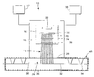
Figure 1 provides a detailed representation of an apparatus constructed in
accordance with the invention, including electron beam source 10 (a single e-
beam
source is represented). Source 10 produces electron beam 11 (e-beam) when high
voltage from high voltage power supply 12 is applied to heated tungsten wire
filaments 14 inside electron gun assembly 16. Gun assembly 16 is positioned
within
vacuum chamber 18 maintained at less than about 10-4 Torr and preferably at
less than
about 10-6 Torr.
Tungsten wire filaments 14 produce electrons 20 that are guided by repeller
plate 22 and extractor grid 24, in the form of beam 11, i.e., a collection of
accelerated
electrons. Repeller plate 22 is typically maintained at a negative charge
potential to
repel and accelerate electrons 20 toward extractor grid 24. Electrons 20 are
accelerated by the beam voltage. i.e., the difference in voltage between
extractor grid
24 and ground. For example, an applied beam voltage of 70 kilovolts (kV)
imparts
energy of 70 kiloelectron volts (keV) to each electron accelerated across the
potential
between the ground and the extractor grid 24.
Electron beam 11 is guided toward terminal grid 26 and subsequently toward
window 28 through which the electrons exit chamber 18 and pass into gap 29.
Gap 29
contains atmosphere 30. After passing through atmosphere 30, the electrons
travel
into material 32 positioned proximate window 28. A moving support (not shown),
sometimes referred to as a web, carries materia132 past window 28. Atmosphere
30
in gap 29 is preferably kept substantially oxygen-free by the influx of
nitrogen from
nitrogen nozzles 34. Beam collector 36 collects any residual electrons. E-beam
processing can be extremely precise when under computer control 38.
The present invention provides an improved method and apparatus for
controlling the penetration of electrons from electron beam source 10 into
material 32.
In doing so, the invention permits improved control of the dose of electrons
absorbed
by specific portions of material 32. The invention identifies and takes
advantage of
the unexpected finding that by using low energy electron beams along with a
low loss
beam path, it is possible to identify parameters where satisfactory coating
doses can be
achieved with a minimum of electron beam penetration into a substrate. In
other
words, the present invention allows for a relatively high dose of electrons at
the upper
9
CA 02384608 2002-02-06
WO 01/16991 PCTIUSOO/20905
portion of the irradiated material, and a relatively low dose of electrons in
the lower
portion of the irradiated material.
The relatively high dose delivered to the coating material, along with the low
dose delivered to the substrate material is achieved by providing an apparatus
that
contains low loss window 28. In addition, gap 29 is preferably small enough to
further reduce energy absorption by atmosphere 30. The combined use of low
loss
window 28 and gap 29 allows the defining of optimum depth/dose relationships
through irradiated materials having varying layered constructions, including
bi-layer
constructions, such as a tape product. Reducing absorption of electrons in gap
29 by
reducing the size of gap 29 also improves efficiency. This effect is most
pronounced
when using beam voltages below 125 keV because, in that range, the gap
accounts for
a greater percentage of energy absorbed regardless of the window material. The
distance of gap 29 between window 28 and materia132 in conventional electron
beam
generators can be from about 2 to 100 millimeters. Adding a spacer element
(not
shown) can place the window closer to the coating surface to achieve a
specified gap.
A spacer element may be positioned between window 28 and the vacuum chamber 18
to lower window 28 or between materia132 and beam collector 36 to raise
materia132
closer to the window, both of which will reduce the size of gap 29. A spacer
element
may be anything that effectively decreases the distance between window 28 and
materia132. Typically it is a metal frame shaped to fit between window 28 and
vacuum chamber 18. The spacer element can typically reduce the atmospheric gap
of
conventional processing equipment from as much as 5 cm to as little as 4 mm or
less.
Adjusting the size of the gap can fine tune the position of the depth/dose
curve
(especially the absorption peak) in relation to the position of materia132.
The optimal
gap size will depend on many factors such as type of window, voltage used,
material
being irradiated. Typically, a preferable gap size for the present invention
is from 2 to
50 mm, more preferably 4 to 10 mm. The general shape of a depth/dose curve is
largely a function of the electron accelerating voltage, which is selected to
provide
adequate modification to material 32 so the material meets the requirements of
a
specific application.
Unit path length is the density of a material (grams per cubic centimeter
(g/cc))
penetrated by an electron beam times the distance (micrometers) being
traversed
(typically the thickness of the material) expressed in units of grams per
square meter
CA 02384608 2002-02-06
WO 01/16991 PCTIUSOO/20905
(gsm). For example, the unit path length of nitrogen gas at standard
temperature and
pressure, having a density of about 0.00125 g/cc is 5 gsm for a gap thickness
of 4 mm,
25 gsm for a gap of 20 mm, and 62.5 gsm for a gap of 50 mm. A nominally 12 m
titanium window has a unit path length of 54 gsm. As can be seen, a large air
gap can
more significantly reduce the penetration of electrons at low voltages than a
conventional titanium window.
Unit path length is conveniently used to compare relative mass stopping power
of various combinations of materials (having different densities and
thicknesses) on a
single scale for a specific voltage. Mass stopping power is the mean energy
loss per
unit path length. The mass stopping power of a material traversed by an
accelerated
electron is affected by beam voltage. Generally mass stopping power is also
directly
related to the density, thickness, and atomic number of the materials being
traversed
by the electron beam. In the present invention, these materials could include
the low
loss window, the gap, the coating, and the substrate.
The present invention provides an apparatus and method that enhances the
ability to control the depth/dose profiles of electron beams in general, and
in particular
low voltage electron beams with energies below 150 keV, including electron
beams
with energies even below 75 keV. In general, this is done by decreasing the
amount
of electron beam energy absorbed before it reaches the material to be
irradiated. The
invention provides a low loss window, preferably comprising a polymeric
material,
and teaches how the window, in combination with a controlled gap size, can
allow for
significant, and advantageous, alterations or adjustments in depth/dose
profiles
through an irradiated material. Through use of a gap having a specified unit
path
length and a window material having a smaller path length than that of, e.g.,
a
conventional nominally 12 micrometer thick titanium windows, the shape of the
depth/dose profile can be altered to make available a greater percentage of
electron
beam energy for modifying the electron beam modifiable coating while avoiding
significant degradation in the underlying electron beam degradable substrate.
For
example, an aluminum vapor coated nominally 25 micrometer thick polyimide
window used with a 2 mm thick nitrogen gap allows twice as much energy to
reach
the coating surface at an operating voltage of 90 kV than a nominally 12
micron thick
titanium window used with a 5 cm nitrogen gap at 125 kV. The metal vapor
coating
on the polyimide has a negligible effect on the unit path length because the
coating is
11
CA 02384608 2002-02-06
WO 01/16991 PCTIUSOO/20905
very thin (about 100 nanometers) and thus has an insignificant unit path
length (less
than 0.5 gsm for each surface that is coated).
Figure 2 is an enlarged representation of window 28, gap 29, and material 32.
Window 28 includes film 41 with upper protective coating or layer 40
(optional) and
lower protective coating or layer 42. Window 28 is supported by a metal grille
(typically referred to as a hibachi) (not shown), which rests against support
43.
Protective coating 40 faces vacuum chamber 18, while protective coating 42
faces
atmosphere 30, which is at about atmospheric pressure. Lower protective layer
42
inhibits free-radical degradation of film 41 initiated by ionization of some
components
of atmosphere 30, such as oxygen. If film 41 is a polymeric material,
protection from
free radical oxidation is particularly beneficial in its useful life, which
makes its use
more practical than shorter-lived windows. Protective layers 40 and 42 can
also
enhance thermal conduction along film 41, thereby assisting in the dissipation
of
excess heat from window 28 during irradiation and reducing strain associated
with
temperature differentials across the width of film 41. In addition, if
protective layers
40 and 42 are sufficiently electrically conductive, they can dissipate
electrical charge
to help resist dielectric rupture of film 41.
Window film 41 may comprise any material that has a unit path length that
allows a low loss beam path to be generated. In other words, it has a small
enough
unit path length that the absorption peak of depth/dose curve for a beam that
passes
through the window can be shifted to the coating layer of a material being
irradiated.
Suitable window materials include aluminum, titanium, beryllium, boron
nitride,
silicon nitride, and silicon. Some windows comprising metallic films may be as
thin
as 2 m or less depending on their strength and flexibility. Some of these
materials
are used in conventional electron beam windows. However, to be useful in a low
loss
beam path, they must be of a thickness that provides a relatively short unit
path length
(in comparison to a conventional window). For example, nominally 12
micrometers
titanium windows are used in conventional electron beam generators. The
inventors
found that the nominally 12 micrometer titanium window they used had an actual
thickness of about 13.97 micrometers. For the present invention, a suitable
titanium
window may have an actual thickness of 12 to 4 micrometers. Various polymeric
films, including polyimide films, are particularly suitable as the window foil
material
12
CA 02384608 2002-02-06
WO 01/16991 PCTIUSOO/20905
because of their small unit path lengths. For example, window foil 41 may
comprise a
nominally 25 micrometer thick film of polyimide, such as a polyimide polymer
that is
the result of a polycondensation reaction between pyromellitic dianhydride and
4,4'diaminodiphenyl ether, available as KAPTON HN from E.I. DuPont de Nemours
and Co., Wilmington, DE, having an actual thickness of about 27.43
micrometers, that
has been aluminum vapor coated, e.g., by sputter coating, on both sides and
has a unit
path length of about 36 grams per square meter (gsm). Other DuPont Kapton
films
may also be suitable. Other polymer materials that may be useful as a low loss
window include those that are heat stable and durable (i.e., having high
tensile
strength and the ability to stretch enough to provide stress releief).
Suitable polymers
may include, for example, aromatic amides, polystyrenes, polysulfones,
polyphenylene sulfides, polyether imides, and polyurethanes. A useful polymer
window preferably has a unit path length of between about 3 and 54 gsm. The
window
may have a thickness of between about 10 micrometers and 40 micrometers,
preferably between 10 and 30 micromters. The more durable the material, the
thinner
the window may be. A thinner window is preferable because it will have a
shorter
unit path length. The window must be strong enough to contain the vacuum
envirorunent of vacuum chamber 18.
Preferably, any protective coating applied to the window material will provide
electrical charge and thermal dissipation as well as free radical oxidation
resistance.
Coatings that provide only electrical or thermal dissipation do not extend the
useful
life of the window to the same degree as a coating that also protects against
free
radical oxidation. Coatings such as silicon dioxide inhibit oxygen attack on
the
polymer film of the window, but do not provide electrical charge dissipation.
On the
other hand, a vapor coated metal such as, for example, aluminum, provide
thermal
dissipation, electrical charge dissipation; and inhibits free radical
oxidation. However,
the metal coatings must be sufficiently thick to be gas impermeable, e.g.,
about 100
nanometers for aluminum. Suitable vapor coating methods are known to those
skilled
in the art. Suitable protective coating materials, in addition to aluminum,
include, for
example, nickel, chromium, and gold.
In addition, protective metal coatings may be coated themselves to prevent
undesirable oxidation which can render the metallic coatings non-conductive or
gas
permeable. For example, a silicon dioxide coating will prevent aluminum from
13
CA 02384608 2002-02-06
WO 01/16991 PCTIUSOO/20905
oxidizing. Protective coating 40 and/or 42 need only be of a material type,
and
thickness, sufficient to be substantially impervious to gas diffusion that
would cause
free radical degradation of the polymer film. By using a low electron-
absorbing
window, even a relatively low voltage electron beam can pass through window 28
with only a small reduction in power. This enables the generation of an
electron beam
having a depth/dose curve suitable to irradiate material 32 in an intensity
sufficient to
provide an adequate dose to modify coating 44 of material 32 without
delivering a
detrimental dose to degradable substrate 46 of material 32.
A dose profile, or gradient, through the cross section of an irradiated
material
such as a coated substrate can be determined by plotting the electron beam
dose at
each increment of distance away from the beam source against the unit path
lengths of
each material the beam traverses. This is illustrated by Figures 4B to 4E.
A dose profile reaches a maximum, or peak, dose at some distance away from
the electron beam source, then decreases with increasing path length. A
conventional
titanium window having a nominal thickness of about 12 micrometers and a unit
path
length of 54 gsm absorbs enough energy that the peak of a depth/dose curve
(i.e., dose
profile) does not move beyond the window/gap regions unless the voltage is
increased
to above 175 kV. This higher voltage typically creates a depth/dose profile
profile
that is flat and wide and slowly decreases through the irradiated material.
Thus, one is
forced to balance having a sufficient dose to modify a coating against having
an
excessive dose that can damage an electron beam degradable substrate. This is
because the shape of the dose profile causes both the coating and substrate to
be
exposed to a dose gradient that declines only gradually. In contrast, the 25-
micrometer thick aluminum vapor coated polyimide film window of the present
invention has a unit path length of only 36 gsm. This allows the peak
absorption to
reach beyond the window region because the window absorbs less energy. The
lower
energy absorption enables the use of low voltages, which can provide steep,
narrow
depth/dose curves. With these steep curves, suitable surface to interface dose
ratios
may be as high as 5:1.
By adjusting beam voltages and gap distances, the dose profile can be
manipulated to place the absorption peak in the modifiable coating layer. In
addition,
the shorter unit path length of the low loss windows of the present invention,
preferably a polyimide window, allows lower voltages to be used. Preferably,
the total
14
CA 02384608 2002-02-06
WO 01/16991 PCT/US00/20905
unit path length of the window, protective layer(s), and gap is less than
about 41 gsm.
The low voltages can provide sharply declining dose profiles beyond the dose
peak.
As a result, the portion of the dose gradient extending into the substrate can
be steep
causing a small dosage to be received by the substrate, thereby limiting
degradation.
The energy absorbed by the substrate is preferably less than 40 percent of the
energy
absorbed by the coating, more preferably less than 25 percent; and most
preferably
less than 20 percent.
Although the phenomenon of the present invention is described as shifting the
peak of a depth/dose curve into a different region, the depth/dose curve for a
given
voltage does not change. However, for a given depth/dose curve, shortening the
unit
path length of a region traversed by the electron beam will cause subsequent
regions,
defined by their unit path length, to be shifted closer to the electron beam
source and,
therefore, closer to the absorption peak. This is illustrated, e.g., by
comparing Figures
4B, 4C, and 4D. As these Figures show, by reducing the unit path length of the
window and gap, the adhesive layer, in terms of unit path length, moves closer
to the
electron beam source.
Monte Carlo code may be effectively used to simulate depth/dose profiles
useful for predicting the effects of various operating conditions on materials
being
irradiated. These predictions allow for anticipating and adjusting the
electron beam
dose at various depths in the irradiated material, and allow for the optimal
dosage
needed to modify a coating on a substrate without excess dosage that can
degrade the
substrate. Suitable Monte Carlo codes include Integrated Tiger Series (ITS),
Electron
Gamma Shower (EGS), and Monte Carlo Neutron-Proton (MCNP). Monte Carlo
code makes it possible to identify an advantageous relationship between dosage
and
depth. The use of Monte Carlo code and related calculations are described in
Douglas
E. Weiss, Harvey W. Kalweit, and Ronald P. Kensek, Low-Voltage Electron-Beam
Simulation Using the Integrated Ti~zer Series Monte Carlo Code and Calibration
Through Radiochromic Dosimetrv, which is Chapter 8 of Irradiation of Polymers,
ACS Symposium Series 620, American Chemical Society, Washington DC 1996. An
alternative method that can be used to calculate depth/dose profiles is
disclosed in
U.S. Pat. No. 5,266,400.
The atomic number of the window material can affect the shape of a
depth/dose curve even when beam voltage is constant. For two materials having
the
CA 02384608 2002-02-06
WO 01/16991 PCTIUSOO/20905
same unit path length, the material having a higher atomic number will cause
more
electrons to scatter. This moves the dose peak closer to the electron beam
source, and
because the electrons still terminate at the same depth for a given unit path
length, this
decreases the negative slope of the post-peak gradient. Figure 3 illustrates
simulated
depth/dose curves through Nylon at three different beam voltages (100, 125 and
175
keV) and a constant gap of 4 micrometers for both a nominally 8 micrometer
thick
titanium window and a nominally 25 micrometer thick polyimide window having a
protective aluminum coating. Both windows have a unit path length of 36 gsm.
As
can be seen, the nominally 8 micrometer thick titanium window having an atomic
number of 12 produces a depth/dose curves having a lower peak dose followed by
a
more gradual gradient decline as compared to depth/dose curves produced by the
nominally 25 micrometer thick polyimide window. Thus, even when the same
interface dose is achieved with a titanium window and a polyimide window
having
equal path lengths, it may be advantageous to use a polyimide window to reduce
energy penetration into a substrate layer.
The low loss windows of the present invention may also be used
advantageously with conventional electron beam generators. Typically it is
most
advantageous with conventional electron beam generators at voltages from about
175
kV up to about 300 kV, especially when curing thick materials. The windows of
the
present invention can provide a broad distance (i.e., depth) over which
identical
surface/interface doses can be achieved. For example, Figure 3 illustrates
that at 175
kV, a 25 micrometer polyimide window can provide a dose of about 5.0
Megaelectronvolts-square centimeter/gram (MeV-cm2/g - source electron) at
distances of 2.54 and 190.5 micrometers (0.1 and 7.5 mils) from the electron
beam
source, whereas the nominally 8 micrometer titanium window only provides a
uniform
dose at 2.54 and 127 micrometers (at a dose of about 7 MeV-cm2/g).
Applications at
a high voltage range might include improving penetration of small bore tubing
or
extending the depth of cure into a thick web of material.
In the present invention, the electron beam radiation used to irradiate the
material has an energy from about 30 to 150 keV in certain embodiments, and
from
about 50 to 75 keV in other embodiments, depending on the equipment being
used.
The electron beam radiation energy is preferably less than 120 keV, more
preferably
less than 100 keV, and most preferably less than 90 keV.
16
CA 02384608 2002-02-06
WO 01/16991 PCT/US00/20905
Figure 4A shows a series of Monte Carlo code depth/dose deposition curves,
over a selected range of voltages, that simulate the dose deposited at various
depths
through water. Water is used here to represent a standard unit-density
material of low
atomic number suitable for predicting energy loss through materials, such as
polymers, having similar densities and components with similar atomic numbers.
The
simulations assumed no window or gap to absorb electrons.
The low-loss window of the present invention can cause the depth/dose curve
to shift and change shape. As indicated in Figure 4A, lower voltage electron
beams
have a higher peak dose, and narrower distribution, than higher voltage
electron
beams. Although the total energy received by the water is less at low voltages
(as
measured by the area under each curve), the energy is received at a shallower
depth.
This allows the dose to be substantially restricted to a narrow band near the
water
surface. As seen in Figure 4A, the depth/dose curve for a 50 keV electron beam
is
substantially between a depth of 0 and approximately 35 grams per square meter
of
the irradiated material. In contrast, for a 130 keV electron beam, which is at
the
higher end of the energy range for the present invention, the depth/dose curve
gradually increases from the water surface until it peaks at around a depth of
95 grams
per square meter, after which it gradually diminishes, trailing off at around
210 gsm.
A low loss beam path is significant because it allows a larger amount of low
voltage electrons to pass through the window, thereby permitting the dose peak
to
move into the adhesive layer. Using the apparatus of the present invention, it
is
possible to adjust the position of the depth/dose curve, in relation to the
depth of the
coating and substrate layers, by varying the electron absorption of the gap
and/or
window so that the coated substrate receives an optimal dose of electrons at
an
appropriate depth to avoid substrate degradation. For example, as shown in
Figure
4A, a 65 keV beam could deliver a sufficient dose to modify the entire coating
thickness of a relatively thin coating (60 gsm). The dose would be delivered
substantially between a depth of approximately 0 and 60 grams per square
meter. Only
a small amount of a substrate, at depths greater than 60 gsm would receive
electron
beam radiation. However, it should be noted that this example does not take
into
account window and gap absorption (it assumed a vacuum, which would absorb no
energy). In actual use, higher voltages would be necessary to compensate for
window
and gap absorption while still achieving the same surface doses as shown in
4A.
17
CA 02384608 2002-02-06
WO 01/16991 PCTIUSOO/20905
Figures 4B through 4E illustrate depth/dose curves through the cross-section
of a typical pressure-sensitive adhesive tape construction irradiated using
different
window and gap combinations. Figure 4B illustrates the shape of a depth/dose
curve
through a conventional nominal 12 micrometer thick titanium window (actual
thickness of about 14, with a unit path length of about 57 gsm), a common 50-
millimeter nitrogen gap (unit path length of about 62 gsm), a 43-micrometer
thick
electron beam crosslinkable pressure-sensitive adhesive (unit path length of
about 40
gsm), and a 127 micrometer thick electron beam degradable non-woven substrate
(unit path length of about 80 gsm).
Figure 4C illustrates the shape of a depth/dose curve through a conventional
nominally 12 micrometer thick titanium window, a narrow 4 millimeter thick
nitrogen
gap (unit path length of about 5 gsm), a 43 micrometer thick electron beam
crosslinkable pressure-sensitive adhesive, and a 127 micrometer thick electron
beam
degradable non-woven substrate.
Figure 4D illustrates the shape of a depth/dose curve through a nominally 3
micrometer thick boron nitride window (unit path length of about 6.8 gsm), a
narrow
4 millimeter thick gap, a 43 micrometer thick electron beam crosslinkable
pressure-
sensitive adhesive, and a 127 micrometer thick electron beam degradable non-
woven
substrate.
Figure 4E illustrates the shape of a depth/dose curve through an aluminum
vapor coated nominally 25 micrometer thick polyimide film window (actual
thickness
of about 27, with a unit path length of about 36 gsm), a narrow 4 millimeter
thick gap,
a 43 micrometer thick electron beam crosslinkable pressure-sensitive adhesive,
and a
127 micrometer electron beam degradable non-woven substrate.
As shown by the above graphs, the dose profile produced with the low voltage
beams used in the present invention is narrower and steeper than with higher
voltage
beams. This profile permits the substrate dose to be significantly less than
the coating
dose. Also, as can be seen by comparing Figures 4B to 4E both the unit path
length of
the window and the thickness of the gap significantly influence the position
of the
depth/dose curve through the irradiated coating and substrate.
A depth/dose profile through a particular irradiated material could be shaped
by exposing the material to a number of beams, each having different voltages.
The
dosage received by the irradiated material at a particular depth would be the
sum of
18
CA 02384608 2002-02-06
WO 01/16991 PCTIUSOO/20905
the doses provided by each beam. A combination of electron beams could be used
to
optimize irradiation patterns for the material being irradiated. For example,
a low
voltage beam, with a very narrow distribution, could be used to supplement or
increase the dose provided to the surface and/or interior of a coating layer
without
providing any additional dose to the coating substrate interface. For thick
irradiated
layers, more than two exposures to various low voltage beams could produce
more
complex profiles. Such multiple exposures could be accomplished by arranging
several compact e-beams in series on an operating line, or by making multiple
passes
with an irradiated material through a single electron beam source.
In addition to preventing degradation in the substrate material, the present
invention can be useful for ensuring that the coating/substrate interface
receives an
adequate electron beam dose to bind the two layers together when necessary.
This can
be important when a strong bond is needed between a coating and an electron
beam
degradable substrate. For example, when an adhesive is applied to a backing,
it is
often important that the adhesive not separate from the backing. The present
invention
can allow the portion of the adhesive at the interface to receive sufficient
electron
beam radiation to ensure a strong bond between the adhesive and backing layer
without exposing the backing to an excessive electron beam dose.
Figure 5 illustrates various depth/dose gradients generated at different
operating conditions, as discussed in the Examples, with the same adhesive and
backing material as in Figures 4B through 4E. The key refers to the gap (e.g.,
4mm),
the window material (PI refers to a nominally 25 m polyimide window and Ti
refers
to a nominally 12 m titanium window), and electron voltage. The profiles
(with
depth indicated in micrometers for each layer) of the adhesive and backing
layers are
given independently to show the surface to interface dose relationships more
clearly
for various window/gap (and voltage) combinations. The space between the
layers
represents the adhesive/backing interface. The currents of the beams were
adjusted to
provide an interface dose of 20 kGy for ease of comparison. As the unit path
length
(as determined by multiplying the density of the material times its thickness)
of the
window/gap combination was increased, voltages were appropriately increased to
maintain acceptable dose gradients through the adhesive layer. The appropriate
voltage could be calculated from Figure 4A, using the method illustrated in
Figures
4B to 4E. The increased voltage caused an increase in total dose received by
the
19
CA 02384608 2002-04-29
60557-6654
backing, which increased its degradation. This degradation can be correlated
to total
energy deposited in the backing, which is represented by the area under the
backing
depth/dose curve. The inventors found that a low loss path using a nominally
25
micrometer polyimide window, a 4 mm gap, and a voltage of 78 kV resulted in no
measurable substrate degradation as determined by the MIT Flex Test (shown in
Tables 6 and 7). (Because the curve in Figure 5 showing the total energy
deposited
with this combination of window, gap, and voltage approaches zero at about 30
micrometers into the depth of the backing, all comparisons were made by
calculating
the energy absorbed from the interface to 30 micrometers into the backing.) As
seen
in Table 7, combination of a nominally 25 micrometer. window (with an actual
thickness of about 27um), a 4 mm gap, and 78 kV voltage, produced total energy
absorption of about 11. 2 mJ/cm? The backing showed no degradation, as
evidenced
by an MIT Flex Number of 1212. When the same window/gap combination was used
with increased voltages, energy absorption increased to 2 5 to 3 5 mj/cm2 and
degradation increased as evidenced by MIT Flex Numbers in the range of 800.
Combinations of window material, gap, and voltage that resulted in less than
10 mi
of energy being absorbed by the backing should produce tapes with good MIT
Flex
Test results.
This invention is not limited to the materials investigated. For example, the
present invention may be used to modify non-adhesive electron beam modifiable
coating materials on electron beam degradable backings. Ethylenically
unsaturated
materials such as acrylates and vinyls, which may be used to make hard coats
and
top coats are examples of such materials. As illustrated in Figures 4A to 4E,
any
combination of window materials and gap distances, when expressed in gsm, and
when coupled with the information provided by the curve shown in Figure 4A
will
allow the calculation of target voltages to achieve the same dose gradients as
in 4A.
Figure 6 shows the depth/dose curve through a tape construction, based on
Monte Carlo simulations, assuming a range of window materials and thickness,
and
a fixed gap of 4 pm. Depth/dose curves were generated for windows comprising
titanium, beryllium, silicon nitride, and boron nitride, using the technique
illustrated
in Figures 4B to 4E. These curves were matched against depth/dose curves from,
Figure 5 for the nominally 25 micrometer thick polyimide window at voltages of
78
and 92 W. Calculations were made to provide about the same interface dose for
CA 02384608 2002-02-06
WO 01/16991 PCTIUSOO/20905
each curve (20 kGy). Figures 5 and 6 allow comparison of different surface to
interface dose ratios. It shows that the ratios can be advantageously
controlled by
window material, gap, and voltage selection. Note that Figure 6 shows that the
depth/dose gradient through the adhesive layer is eventually reduced as the
unit path
length for the window is reduced and the dose peak is allowed to move into the
adhesive layer. For example, the depth/dose gradient for a 65 keV beam through
a
3 micrometer thick boron nitride window has nearly equal entrance and exit
doses in
the adhesive layer with the same minimal penetration into the paper as
observed for
a 78 keV beam through a 25 micrometer polyimide window, which has an entrance
dose five times greater than exit dose. The similar entrance/exit doses may
allow
for a customized balance of modification (such as crosslinking) through the
depth of
an adhesive layer without increasing damage to the substrate. This, in turn,
could
allow for a customized balance of adhesive properties, e.g., peel and shear,
to
provide a tape with properties customized to its intended use.
For some embodiments of the invention, such as the adhesive tape
construction used in the Examples, the intensity of electron beam radiation
received
by the coating surface may be between about 1 and 5 times greater than the
intensity
of electron beam radiation received by the substrate surface. For other
embodiments, a
ratio as high as 5:1 will adversely modify the surface of the coating layer,
e.g., over-
crosslink or degrade the coating layer. An ideal depth/dose curve for a tape
construction can be determined by selecting a combination of window material
and
gap distance that provides the dose profile through the layers needed to
obtain
optimum tape properties. Typical measured properties for paper-backed pressure-
sensitive adhesive tapes, such as those in the examples, are 5-bond (cohesive
strength
of adhesive), holding power (slow rate peel resistance), and MIT flex (folding
endurance test, the results of which are sensitive to degradation of the
backing).
Combinations of electron beam modifiable coatings and electron beam
degradable backings other than those specifically disclosed herein will have
different
optimum voltages, gaps, and interface doses for achieving desired
modifications.
However, the optimum values can be determined by one skilled in the art based
on the
teachings herein, for example by knowing the thicknesses and densities of the
materials used and applying this information to Figure 4A.
The low loss path of the present invention can provide increased material
21
CA 02384608 2002-02-06
WO 01/16991 PCT/US00/20905
throughput during production. The low loss path causes less interaction
between the
electrons and the window and gap materials than in a conventional electron
beam
path, thereby making available a greater dose to the surface of the coating.
While specific examples have been used to illustrate the invention, the
invention is not limited to the particular embodiments described, but rather
covers
modifications, equivalents, and alternatives falling within the spirit and
scope of the
appended claims.
EXPERIMENTAL SECTION
The following experiments were conducted to demonstrate effective
parameters for operation of the apparatus of the invention. Tables 1 through 5
provide
a summary of the results of irradiation of dosimeters at five different target
coating/substrate interface dosages: 20, 40, 60, 80 and 100 kGy. The window
material, voltage, gap, and current were all varied to assess the impact of
altering
these variables. In addition, tests on the physical properties of materials
irradiated in
accordance with the invention are provided in Tables 6, 7 and 8. Comparative
data,
obtained using a conventional nominally 12 micrometer titanium window, are
also
included in the tables.
For these experiments, the radiation processing was performed on an Energy
Sciences, Inc. Model CB-175 electron beam generating apparatus equipped with a
six-
inch wide support (web) running through an inert chamber. Samples of coated
substrates were conveyed on the web at a speed of 3.1 meters per minute. The
oxygen
level within the chamber of the CB-175 was restricted to a range of 50 to 100
ppm.
The standard nitrogen gap between the window and web path (using original
equipment) of the CB-175 is 18 mm. To reduce this nitrogen gap distance,
spacers
were added between the vacuum chamber and the window support. For example, to
create a 4-mm thick nitrogen gap, a 14-mm thick spacer was placed between the
vacuum chamber and the window support. Upon installation of the spacer, a 3-mm
thick low profile window clamp was used to maintain the window in place on the
electron beam generating apparatus. This low profile clamp was a substitute
for an
original 10-mm thick standard clamp. This substitution was made to provide
adequate
clearance past the clamp for the irradiated substrate.
To calibrate the CB- 175, extensive dosimetry was done using both 45 micron
22
CA 02384608 2002-02-06
WO 01/16991 PCTIUSOO/20905
and 10 micron dosimeters, which are polymeric films containing radiochromic
dye,
available from Far West Technologies, Inc., Goleta, CA. Dosimetry was
performed at
kV increments, from 90 to 180 kV, for both polyimide and titanium windows. The
titanium window material (having a nominal thickness of 12 m ) was found to
be
5 13.97 m thick, and the polyimide film, (previously available as Kapton E,
believed to
be the equivalent of currently available KAPTON HN (a polyimide polymer that
is the
result of a polycondensation reaction between pyromellitic dianhydride and
4,4'diaminodiphenyl ether), available from DuPont and sold at a nominal
thickness of
25.4 m (1 mil)) was found to be 27.43 microns thick, including a 100-
nanometer
10 thick aluminum coating on each side. In all cases, three each of the 10 and
45
micrometer dosimeters were mounted onto index cards, which were attached to
the
moving web, and irradiated. The dose at each voltage for each dosimeter
thickness
was determined by averaging the three readings obtained. The dosimetry data
was
used to compare the actual instrument dose to the indicated instrument current
in
order to determine and adjust the actual power of the CB-175.
The individual depth/dose relationship at each voltage was determined from an
average of three dosimeter stacks. Stacks of the 10 m dosimeters were
typically used
for low voltages and the 43.5 m dosimeters were typically used for high
voltages,
e.g., above about 125 kV. The actual voltage was determined by comparing the
stepped depth/dose profiles of the dosimeter stacks to Monte Carlo simulations
of
these stacks over a range of voltages. The CB-175 actual electron beam voltage
was
consistently 90% of the indicated voltage, and this information was used to
provide
corrected voltages. All voltages referred to in this document are the
corrected
voltages.
Masking tape samples were used to generate the testing data shown in Tables
6 to 9. The tape comprised an adhesive coating on a fabric backing. The
adhesive
comprised one or more electron beam crosslinkable elastomers and one or more
tackifying resins with no additional curing additives and had a layer
thickness of 40.6
micrometers and a specific gravity of 0.93. The tape backing was a cellulose-
based
non-woven fabric approximately 107 micrometers thick with a specific gravity
of
0.63. The tape was made by extruding the adhesive layer onto the backing.
Measured doses were compared to calculated doses obtained by Monte Carlo
23
CA 02384608 2002-02-06
WO 01/16991 PCTIUSOO/20905
code for identical cross-sections to validate the code predictions. All
calculations
were made using actual material thicknesses (e.g., the nominally 12 m
titanium
window was actually about 13.97 m thick, so 14 m was used for the
calculations;
and the nominally 25 m thick Kapton window was actually about 27.43 gm thick,
so
27 m was used for calculations). The inventors found it was important to use
actual
measurements rather than nominal thicknesses and actual voltages rather than
indicated voltages to obtain simulations that reconciled with measured values;
this
appears to be especially important when operating at low voltages. Monte Carlo
code
was also used to calculate currents needed at selected voltages to provide
doses of 20,
40, 60, 80 and 100 kGy at the interface of the adhesive and the backing. The
results
are shown in Tables 1 through 5. The 10 m dosimeter approximated the adhesive
surface. The 43.5 m dosimeter approximated the total bulk of the adhesive and
was
used to approximate the adhesive/backing interface. In most cases, the results
of the
measured and calculated doses were within 20 percent of one another, and only
in a
few cases was the variance greater than 20 percent, for reasons that are not
known. It
is believed this high error margin is partially due to instabilities caused by
operating
the machinery below the voltage range it was designed for (approximately 150
to 175
kilovolts) and at a low current (less than 1 milliamp (mA)).
Table 1 shows the calibrations needed to obtain a targeted interface dose of
20
kGy. Examples 1 through 10 show 20 kGy targeted doses at gap distances of 4,
17,
and 47 mm for a nominally 25 m polyimide window having a protective 100
nanometer aluminum coating. Compartive Examples 11 and 12 show 20 kGy targeted
doses at a gap distance of 17 mm for a nominally 12 m titanium window. The
voltage was varied for the examples from a low of 78 kV to a high of 139 kV
for the
polyimide windows; and from 114 to 146 kV for the titanium window. The current
was also varied from a maximum of 0.63 rnA to a minimum of 0.22 mA (the range
varied for each window/gap combination).
As the voltage was increased, the depth/dose gradient decreased. To
compensate, the current was decreased to obtain the same target interface
dosage at
each voltage for each window material. Example 1 of Table 1 used a 78 kV
voltage
and a 0.63 mA current to obtain a targeted 20 kGy dose at the adhesive/backing
interface. The calculated dose at a depth of 10 micrometers was 76 kGy and the
24
CA 02384608 2002-02-06
WO 01/16991 PCTIUSOO/20905
measured dose was 59 kGy; the calculated dose at 43.5 micrometers was 43 kGy
and
the measured dose was 29 kGy. In contrast, example 4 of Table 1 used an 87 kV
voltage and a 0.27 mA current to obtain a targeted 20 kGy dose at the
interface. The
calculated dose at a depth of 10 micrometers was 32 kGy and the measured dose
was
26 kGy; the calculated dose at 43.5 micrometers was 24 kGy and the measured
dose
was 14 kGy. Comparing examples 1 and 4 of Table I demonstrates that increasing
the voltage and lowering the current produces a lower measured dose at both 10
and
43.5 micrometers. Similar correlation trends are identified in the other Table
1
examples.
Table 1 also indicates that it is possible to achieve a greater difference
between
the dose near the surface of the irradiated material (10 m) and the interior,
e.g., the
coating/substrate interface, of the material (43.5 m) when a nominally 25 m
polymeric (polyimide, in this case) window is used rather than a conventional
nominally 12 m titanium window. This greater difference indicates that peak
absorbance is shifting into the irradiated material. Specifically, in
reference to Table
1, examples 7 and 11 both use a gap of 17 mm, but example 7 uses a nominally
25 m
polyimide window while example 11 uses a nominally 12 m titanium window. The
polyimide window has a shorter unit path length. In example 7 the measured
dose at
the10 micrometer depth was approximately 1.7 times greater than at the 43.5
micrometer depth. In contrast, in example 1 I the measured dose in the 10
micrometer
dosimeter was only slightly more than 1.2 times greater than the 43.5
micrometer
dosimeter. Thus, the use of a low loss polyimide window can improve
performance
by increasing the dose in the adhesive portion of the irradiated material
relative to the
backing portion of the material, thereby avoiding degradation to the backing
material.
In summary, Table 1 shows the relationship of surface dose (10 m) to total
dose through the adhesive layer (43.5 m) at a targeted interface dose of 20
kGy. The
surface dose increases as the peak of the depth/dose curve moves away from the
window and into the coating layer to be irradiated. This occurs as the unit
path length
of the window and gap regions are decreased, and lower voltages are used to
achieve
or approach a targeted interface dose. Lower voltages correlate to a sharp
decline in
dose gradient through the backing material.
CA 02384608 2002-02-06
WO 01/16991 PCT/US00/20905
In addition, because the adhesive layer can receive a higher dose at a lower
voltage with the present invention, the coated substrate may be processed
faster than
with a conventional system that uses nominally 12 micrometer metallic windows,
a 50
mm wide gap, and the same current settings. The difference can be observed,
for
example by comparing Example 3 to Comparative Example 11, both of Table 1.
Example 3 uses a nominally 25 m polyimide window, a 4 mm gap, 82 kV voltage,
and a 0.40 mA current, and provides a measured dose of 29 kGy at 10 m.
Comparative Example 11 uses a nominally 12 m titanium window, a 17 mm gap,
114 kV voltage, and a 0.41 mA current, and provides a measured dose of 17 kGy
at 10
m. Because the present invention allows for a higher surface dose at a given
current,
it allows for a higher throughput of material being irradiated, even when the
electron
beam generator is operating at maximum current.
26
CA 02384608 2002-02-06
WO 01/16991 PCTIUSOO/20905
Table 1
Targeted Interface Dose: 20 kGy
Example Gap Window Voltage Current Depth Calculated Measured
Distance Material (kV) (mA) ( m) Dose Dose
(mm) (kGy) (kGy)
1 4 Polyimide 78 0.63 10 76 59
4 Polyimide 43.5 43 29
2 4 Polyimide 80 0.51 10 62 51
4 Polyimide 43.5 38 39
3 4 Polyimide 82 0.40 10 47 29
4 Polyimide 43.5 31 23
4 4 Polyimide 87 0.27 10 32 26
4 Polyimide 43.5 24 14
4 Polyimide 92 0.22 10 25 21
4 Polyimide 43.5 21 15
6 4 Polyimide 101 0.21 10 21 23
4 Polyimide 43.5 19 12
7 17 Polyimide 98 0.29 10 30 19
17 Polyimide 43.5 24 11
8 17 Polyimide 116 0.23 10 17 21
17 Polyimide 43.5 19 21
9 47 Polyimide 118 0.33 10 29 24
47 Polyimide 43.5 23 24
47 Polyimide 139 0.25 10 21 17
47 Polyimide 43.5 20 20
CE 11 17 Ti 114 0.41 10 29 17
17 Ti 43.5 22 14
CE 12 17 Ti 146 0.29 10 22 18
17 Ti 43.5 21 17
Table 2, below, shows the affect on 10 micrometer dosimeters and 43.5
5 micrometer dosimeters of changes in gap distance, window material, voltage,
and
current used to obtain a target interface dose of 40 kGy. As in Table 1, the
greatest
27
CA 02384608 2002-02-06
WO 01/16991 PCT/US00/20905
difference between the dose near the surface (10 micrometer) and the dose
through the
entire irradiated adhesive material {43.5 micrometer) are accomplished with a
low loss
window. In particular, the greatest dosage difference is achieved when the low
loss
nominally 25 m polyimide window having a 100 nm thick aluminum protective
coating is combined with a small gap distance. Example 1 of Table 2 shows that
the
polyimide window, in conjunction with a 4 mm nitrogen gap, provided a measured
dose of 147 kGy in the 10 micrometer dosimeter, and a measured dose of 70 kGy
in
the 43.5 micrometer dosimeter. These results were achieved by using a 78 kV
voltage
and 1.26 mA current. Example 2 shows similar results with a 80 kV voltage and
1.02
mA current producing a measured dose of 121 kGy in the 10 micrometer
dosimeter,
and a measured dose of 66 kGy in the 43.5 micrometer dosimeter. The difference
in
measured dose at 10 versus 43.5 micrometers generally diminishes as the gap
increases. For example, Example 10, which used a47 mm gap with a 139 kV
voltage
and 0.49 mA current, shows that the measured doses at 10 and 43.5 micrometers
were
39 and 41, respectively.
The contrast between using the polyimide window having a protective coating
together with a small gap and using the 12 m titanium window together with a
larger
gap is clearly indicated by comparing examples 3 and 11 of Table 2. In example
3,
which used the polyimide window and a 4 mm gap, a voltage of 82 kV, and
current of
0.80 mA produced a measured dose of 94 kGy in the 10 micrometer dosimeter and
45
kGy in the 43.5 micrometer dosimeter. In contrast, example 11, which used a 12
m
titanium window and a 17 mm gap with a higher voltage of 114 kV and same
current
of 0.81 mA, achieved a measured dose of only 38 kGy in the 10 micrometer
dosimeter
and 32 kGy in the 43.5 micrometer dosimeter. These examples demonstrate that
the
shorter unit path length of the polyimide window/small gap as compared to the
conventional titanium window/large gap shifts the absorption peak of the
depth/dose
curve away from the electron beam source toward the adhesive layer. This
higher dose
provided to the adhesive layer represents a more efficient use of the electron
beam.
The comparison also indicates that the low loss beam path results in a
significantly
higher surface to interface dose ratio. This is indicative of a desirable
steeper
depth/dose gradient through the backing layer.
28
CA 02384608 2002-02-06
WO 01/16991 PCT/US00/20905
Table 2
Target Interface Dose: 40 kGy
Example Gap Window Voltage Current Depth Calculated Measured
Distance Material (kV) (mA) ( m) Dose Dose
(mm) (kGy) (kGy)
1 4 Polyimide 78 1.26 10 153 147
4 Polyimide 43.5 87 70
2 4 Polyimide 80 1.02 10 124 121
4 Polyimide 43.5 75 66
3 4 Polyimide 82 0.80 10 95 94
4 Polyimide 43.5 63 48
4 4 Polyimide 87 0.53 10 64 53
4 Polyimide 43.5 48 31
4 Polyimide 92 0.44 10 49 40
4 Polyimide 43.5 42 32
6 4 Polyimide 101 0.43 10 43 45
4 Polyimide 43.5 41 31
7 17 Polyimide 98 0.57 10 61 50
17 Polyimide 43.5 47 38
8 17 Polyimide 116 0.45 10 42 40
17 Polyimide 43.5 41 40
9 47 Polyimide 118 0.65 10 58 57
47 Polyimide 43.5 45 49
47 Polyimide 139 0.49 10 42 39
47 Polyimide 43.5 39 41
CE 11 17 Ti 114 0.81 10 58 38
17 Ti 43.5 45 32
CE 12 17 Ti 146 0.58 10 45 36
17 Ti 43.5 41 40
Tables 3, 4, and 5 show correlations similar to those in Tables 1 and 2.
Tables 3, 4,
5 and 5 generally demonstrate a high surface to interface dose ratio for the
coating layer
(approximated by the 10 micrometer dosimeter (surface) and 43.5 micrometer
29
CA 02384608 2002-02-06
WO 01/16991 PCT/US00/20905
dosimeter(interface)) when the low loss electron beam path is used, especially
at
lower voltages. The tables also demonstrate increased energy efficiency when
using
the low loss electron beam path as indicated by the higher surface dose
achieved as
compared to the Comparative Examples, having similar current settings. For
example, in Table 3, Example 7 uses the nominally 25 micrometer polyimide
window
and a current of 0.86 mA while Comparative Example 12 uses the conventional
nominally 12 micrometer titanium window and a current of 0.88 mA. Example 7
requires a voltage of only 98 kV to achieve a measured surface dose (at 10 m)
of 97
kGy while Comparative Example 12 requires a voltage of 146 kV to achieve a
measured surface dose of 53 kGy.
CA 02384608 2002-02-06
WO 01/16991 PCT/US00/20905
Table 3
Target Interface Dose of 60 kGy
Example Gap Window Voltage Current Depth Calculated Measured
Distance Material (kV) (mA) ( m) Dose Dose
(mm) (kGy) (kGy)
1 4 Polyimide 78 1.89 10 229 266
4 Polyimide 43.5 130 113
2 4 Polyimide 80 1.53 10 187 199
4 Polyimide 43.5 113 100
3 4 Polyimide 82 1.20 10 143 153
4 Polyimide 43.5 94 84
4 4 Polyimide 87 0.80 10 96 67
4 Polyimide 43.5 73 51
4 Polyimide 92 0.66 10 74 69
4 Polyimide 43.5 63 54
6 4 Polyimide 101 0.64 10 64 74
4 Polyimide 43.5 62 62
7 17 Polyimide 98 0.86 10 91 97
17 Polyimide 43.5 71 73
8 17 Polyimide 116 0.68 10 63 62
17 Polyimide 43.5 62 61
9 47 Polyimide 118 0.98 10 87 85
47 Polyimide 43.5 68 68
47 Polyimide 139 0.74 10 63 60
47 Polyimide 43.5 59 66
CE 11 17 Ti 114 1.22 10 87 57
17 Ti 43.5 67 49
CE 12 17 Ti 146 0.88 10 67 53
17 Ti 43.5 62 64
31
CA 02384608 2002-02-06
WO 01/16991 PCTIUSOO/20905
Table 4
Targeted Interface Dose of 80 kGy
Example Gap Window Voltage Current Depth Calculated Measured
Distance Material (kV) (mA) ( m) Dose Dose
(mm) (kGy) (kGy)
1 4 Polyimide 78 2.52 10 305 350
4 Polyimide 43.5 173 143
2 4 Polyimide 80 2.04 10 249 293
4 Polyimide 43.5 150 139
3 4 Polyimide 82 1.60 10 190 231
4 Polyimide 43.5 125 110
4 4 Polyimide 87 1.08 10 128 134
4 Polyimide 43.5 97 90
4 Polyimide 92 0.88 10 98 105
4 Polyimide 43.5 84 82
6 4 Polyimide 101 0.84 10 84 97
4 Polyimide 43.5 81 87
7 17 Polyimide 98 1.16 10 123 119
17 Polyimide 43.5 96 82
8 17 Polyimide 116 0.92 10 85 92
17 Polyimide 43.5 84 80
32
CA 02384608 2002-02-06
WO 01/16991 PCTIUSOO/20905
Table 5
Targeted Interface Dose: 100 kGy
Example Gap Window Voltage Current Depth Calculated Measured
Distance Material (kV) (mA) ( m) Dose Dose
(mm) (kGy) (kGy)
1 4 Polyimide 78 3.15 10 381 440
4 Polyimide 43.5 216 165
2 4 Polyimide 80 2.55 10 311 378
4 Polyimide 43.5 187 177
3 4 Polyimide 82 2.00 10 237 286
4 Polyimide 43.5 156 157
4 4 Polyimide 87 1.35 10 160 176
4 Polyimide 43.5 121 115
4 Polyimide 92 1.10 10 123 137
4 Polyimide 43.5 105 100
6 4 Polyimide 101 1.05 10 105 119
4 Polyimide 43.5 102 113
7 17 Polyimide 98 1.45 10 153 158
17 Polyimide 43.5 120 105
8 17 Polyimide 116 1.15 10 107 116
17 Polyimide 43.5 104 104
In addition to the dosimetry measurements, samples of irradiated masking tape
5 were analyzed for performance characteristics. After irradiation, the
adhesive side of
the samples was immediately covered with the low adhesion backsize side of a
tape
backing. All samples were stored in a constant humidity/temperature room (50%
relative humidity, 21 C) for a minimum of 48 hours before being tested. The
samples
were tested in accordance with the following standardized tests:
(1) MIT flex test. Tests were conducted on a 12.5 mm wide strip of tape
using an MIT Flex Tester Model #1 made by Tinius Olsen Testing Machine Company
of Willow Grove, PA. The sample was mechanically flexed under a tension from a
suspended weight of 1.5 kg until the tape broke. Each reported result is an
average of
3 measurements with the reported result having a variability of +/- 20
percent.
33
CA 02384608 2002-02-06
WO 01/16991 PCTIUSOO/20905
Degradation of the backing was measured by comparing the number of flex
repetitions
to failure to that of an unirradiated saturated and strengthened crepe paper
backing.
An unirradiated backing typically survives 1200 flexes. A flex repetition of
900 to
1200 was considered very good with substantially no degradation present. Tape
having a flex repetition of between 900 and 600 was considered satisfactory
for many
current applications. Tape having a flex repetitions of between 600 and 300
was
considered satisfactory for some current applications such as removing the
tape from a
substrate without its breaking or tearing. Tape having a flex repetition rate
of below
300 was considered unacceptably brittle for most applications.
(2) 5-bond test. The 5-bond test measures the cohesive strength of an adhesive
by means of a hanging shear test. Two 12.5-mm wide strips of tape were joined
on
their adhesive sides over a 12.5-mm length. A 4.4 kg roller was then passed
six times
over the joined area. The joined strips were then mounted vertically in a jig
with a
1000 gram weight attached to and suspended from the lower end of the sample.
The
time it took for the strips to separate was measured (in minutes). Tests were
terminated any time after 5000 minutes. For adhesive-backing combinations used
in
this study, times over 400 minutes generally indicate satisfactory
crosslinking and
under times 400 minutes generally indicate unsatisfactory (not enough)
crosslinking.
(3) Holding power. The holding power test measures the time it takes for a
tape, having a specified weight attached, to separate from a polished
stainless steel
plate held in a horizontal position. One end (10 cm long) of a 15 cm long by
19.1 mm
wide tape was attached to the plate by passing a 9.9 kg roller over the 10 cm
section
six times. The plate with tape was then mounted horizontally with the free
tape end
hanging down to create a 90 degree peel angle. A 200 gram weight was attached
to
the free tape end. The time it took for the tape to separate from the plate
was
measured (in minutes). A holding time of at least 30 minutes was judged
satisfactory.
The reported results of the above tests were each an average of three
measurements.
It is desirable to obtain high values for the MIT Flex Test, 5 Bond, and
Holding Power Data. High values indicate that the tested samples are flexible
and
have high bond strength.
Table 6, below, provides MIT flex test data for masking tape samples. As
described in the beginning of the Examples section, the masking tape comprised
an
34
CA 02384608 2002-02-06
WO 01/16991 PCTIUSOO/20905
adhesive coating on a fabric backing. The tape constructions were irradiated
in a
nitrogen atmosphere using the window materials, gap distances, voltages and
currents
shown in Tables 1 through 5. The MIT flex test results shown in Table 6
demonstrate
that the flex propertv of the tape samples was sensitive to both the depths of
the
electron beam penetration (which directly correlates to voltage levels) and to
the
intensity of the radiation (which directly correlates to dose levels). As seen
in Table
6, the most favorable results correlated a 4 mm gap and a nominally 25 m
polyimide
window used with voltages of under 100 kV and particularly under 80 kV at
interface
doses of 20 to 60 kGy. Table 6 also shows that even at a targeted interface
dose of
100 kGy, the MIT Flex Test numbers were generally between 1000 and 600. Table
6
further indicates that a targeted interface dose of as little as 20 kGy
produced
satisfactory adhesive tape from the adhesive and backing material used.
Table 6
MIT Flex Data at Various Dosage
Apparatus Interface Dosage
Gap Window Voltage 20 40 60 80 100
(mm) (material) (kV) (kGy) (kGy) (kGy) (kGy) (kGy)
Cycle Numbers
4 polyimide 78 1212 1171 873 831 967
4 polyimide 80 1123 902 952 618 757
4 polyimide 82 868 874 908 796 706
4 polyimide 87 1080 893 882 857 826
4 polyimide 92 807 1098 1003 826 606
17 polyimide 98 804 857 778 755 705
4 polyimide 101 895 1093 909 575 493
17 titanium 114 920 982 844 --- ---
17 polyimide 116 851 608 537 461 442
47 polyimide 118 860 748 648 --- ---
47 polyimide 139 769 558 405 --- ---
17 titanium 146 728 495 343 --- ---
CA 02384608 2002-04-29
60557-6654
Table 7 tabulates the data illustrated in Figure 5. The currents of the
generated
depth/dose curves were adjusted to provide an interface dose of 20 kGy for a
low loss
path using a 4 mm nitrogen gap and a 27 m (nominally 25 in) thick polyimide
window having a 36 gsm unit path length. To obtain the 20 kGy interface dose
without excessively modifying the adhesive surface, e.g., overcrosslinking, 78
kV was
the lowest practical voltage because a lower voltage would create a surface to
interface dose ratio greater than 5 to 1, which could cause excessive
modification of
the surface. At a 78 kV voltage, there was no detectable paper degradation as
indicated by the MIT Flex Test Cycle Number of 1212. As the voltage was
increased
for the same combination of window, gap, and interface dose, the general trend
of the
Flex Test Numbers decreased, indicating an increase in backing degradation.
Backing
degradation generally increased as voltage increased and as the gap was
changed from
4 mm to 17 mm, then 47 mm, which is near the 50 mm gap typical of commercially
available electron beams. Backing degradation was also higher when a
conventional
14 micrometer thick titanium window was used (at voltages of 114 and 146
kV) with a 17 mm gap.
Degradation, as represented by the Flex Test Numbers of Table 7 roughly
correlate to total energy deposited in the fn-st 30 micrometers of the backing
material.
Total energy deposited is represented by the area under the depth/dose
curve.of Figure
5. As seen in Table 7, energy absorption on the order of about 11. 2 mJ/ cm2
over the
first 30 tnicrometers of the backing produced no degradation. When about 2 5
to 3 5
mi/ cm2 were absorbed over this same distance, the degradation became more
significant (with flex numbers decreasing to about 700 to 800 cycles).
Therefore, it is
preferable to keep the. energy absorbed within the first 30 m of the backing
layer
below about 4 0 mJ/ cm2 .
36
CA 02384608 2002-04-29
60557-6654
Table 7
Backing Energy Absorption vs. Flex Test Numbers
window gap voltage energy MIT Flex Number
(actual thickness) mm kV mJ/cm2
27 micron polyimide 4 78 11.2 1212
27 micron polyimide 4 80 12.7 1123
27 micron polyimide 4 82 15.7 868
27 micron polyimide 4 87 21.3 1080
27 micron polyimide 4 92 25.4 807
27 micron polyimide 4 101 32.1 895
27 micron polyimide 17 98 25.1 804
27 micron ol imide 17 116, 34.5 851
27 micron polyimide 47 118 27.5 860
27 micron 1 imide 47 139 33.7 769
14 micron titanium 17 114 27.4 920
14 micron titanium 17 146 34.5 728
Table 8 provides 5-bond test data. The 5-bond results were a function of
interface dose independent of voltage. As dose was increased, 5-bond results
increased under all window, gap, and voltage conditions, until the results
eventually
exceeded 5000 minutes. Testing was terminated after the sample exceeded 5000
minutes. Hence, Table 8 indicates that the 5-bond property of a tape can be
controlled
by adjusting voltage at a constant target interface dose. A dose of 20 kGy was
usually
sufficient to produce results of about 500 minutes and a dose of 40 kGy was
usually
sufficient to produce results of about 5,000 minutes
37
CA 02384608 2002-02-06
WO 01/16991 PCT/US00/20905
Table 8
Bond Data
Apparatus Interface Dosage
Gap Window Voltage 20 40 60 80 100
(mm) (material) (kV) (kGy) (kGy) (kGy) (kGy) (kGy)
Minutes to Fail
4 polyimide 78 742 4390 4844 5000+ 5000+
4 polyimide 80 1716 5000+ 5000+ 5000+ 5000+
4 polyimide 82 670 3553 5000+ 5000+ 5000+
4 polyimide 87 235 1220 4865 5000+ 5000+
4 polyimide 92 314 1326 5000+ 5000+ 5000+
17 polyimide 98 258 4253 5000+ 5000+ 5000+
4 polyimide 101 626 3372 5000+ 5000+ 5000+
17 titanium 114 330 1485 5000+ --- ---
17 polyimide 116 618 3730 5000+ 5000+ 5000+
47 polyimide 118 675 2816 5000+ --- ---
47 polyimide 139 516 3192 5000+ --- ---
17 titanium 146 210 5000+ 5000+ --- ---
Table 9 provides holding power test results. As expected, holding power
5 appeared to be very sensitive to surface dose. Increasing the targeted
interface dose,
which also increased surface dose lowered the holding power. The general data
trend
shows that lower holding power correlates to higher interface dosage. As seen
in
Tables 1 to 5, voltages below about 92 kV can introduce a high surface dose
relative
to interface dose. This can cause the surface to be over-modified, e.g., over-
cured or
over-crosslinked, which can result in low holding power.
38
CA 02384608 2002-02-06
WO 01/16991 PCTIUSOO/20905
Table 9
Holding Power Data
Apparatus Interface Dosage
Gap Window Voltage 20 40 60 80 100
(mm) (material) (kV) (kGy) (kGy) (kGy) (kGy) (kGy)
Minutes to Fail
4 polyimide 78 64 26 25 7 5
4 polyimide 80 14 12 8 5 6
4 polyimide 82 60 38 23 9 7
4 polyimide 87 99 82 45 18 10
4 polyimide 92 130 63 47 19 16
17 polyimide 98 128 74 45 18 13
4 polyimide 101 93 67 54 15 15
17 titanium 114 110 114 74 --- ---
17 polyimide 116 107 80 42 17 17
47 polyimide 118 100 78 58 --- ---
47 polyimide 139 65 72 68 --- ---
17 Titanium 146 83 111 76 --- ---
The data from Tables 6, 8 and 9 indicate that a broad range of voltage/dose
combinations for low loss paths can produce a masking tape that satisfies
performance requirements. A low loss beam path at voltages as low as 90 kV or
less can provide tape properties that exceed minimum requirements for most
applications.
Other embodiments of the invention are within the scope of the following
claims. It is intended that the specification and examples be considered as
exemplary
only, with the full scope and spirit of the invention being indicated by the
following
claims.
39