Note: Descriptions are shown in the official language in which they were submitted.
CA 02384889 2002-03-12
WO 01/24228 PCTIUSOO/26355
APPLICATION FOR PATENT
TITLE: TEMPORARY BRIDGE FOR MICRO MACHINED
STRUCTURES
INVENTORS: LIANZHONG YU
HOWARD D. GOLDBERG
DULI YU
Background of the Invention
This invention relates to micro-machined structures and, more particularly, to
methods and apparatus for manufacturing micro-machined structures.
Micro machined structures are used to provide components for use in, for
example, strain gauges, accelerometers, and gyroscopes. Typically such
components are manufactured by micro machining a silicon substrate using a
sequence of photolithographic processes including the steps of masking and
etching
pre-selected sections of the silicon substrate to produce a three dimensional
structure. The three dimensional structures produced from the silicon
substrate are
often extremely fragile and can easily become damaged during the manufacturing
process.
The present invention is directed to overcoming or at least minimizing the
limitations of the conventional manufacturing processes for producing micro
machined structures.
Summary of the Invention
According to one aspect of the present invention, a micro machined
apparatus is provided that includes a support structure, one or more temporary
CA 02384889 2002-03-12
WO 01/24228 PCT/US00/26355
bridges coupled to the support structure, and a mass coupled to the temporary
bridge.
According to another aspect of the present invention, a method of
manufacturing a micro machined apparatus is provided that includes micro
machining a support structure coupled to a mass using one or more temporary
bridges in a substrate and severing the temporary bridges.
According to another aspect of the present invention, a method of fabricating
a micro machined structure is provided that includes providing a top silicon
wafer
and a bottom silicon wafer, forming a cavity in the bottom surface of the top
silicon
wafer, bonding the top silicon wafer onto the bottom silicon wafer, etching a
portion
of the top surface of the top silicon wafer, and micro machining a three
dimensional
structure in the portion of the top silicon wafer above the cavity having one
or more
temporary bridges for coupling the three dimensional structure to the
remaining
portions of the top silicon wafer.
According to another aspect of the present invention, a method of fabricating
a micro machined structure is provided that includes providing a top silicon
wafer
and a bottom silicon wafer, forming a cavity in the top surface of the bottom
silicon
wafer, bonding the top silicon wafer onto the bottom silicon wafer, etching a
portion
of the top silicon wafer and micro machining a three dimensional structure in
the
portion of the top silicon wafer above the cavity having one or more temporary
bridges for coupling the three dimensional structure to the remaining portions
of the
top silicone wafer.
2
CA 02384889 2002-03-12
WO 01/24228 PCT/USOO/26355
According to another aspect of the present invention, a method of fabricating
a micro machined structure is provided that includes providing a top silicon
wafer
having an internal layer of silicon dioxide and a bottom silicon wafer,
forming a
cavity in the bottom surface of the top silicon wafer, bonding the top silicon
wafer
onto the bottom silicon wafer, etching a portion of the top surface of the top
silicon
wafer, and micro machining a three dimensional structure in the portion of the
top
silicon wafer above the cavity having one or more temporary bridges for
coupling the
three dimensional structure to the remaining portions of the top silicon wafer
According to another aspect of the present invention, a method of fabricating
a micro machined structure is provided that includes providing a top silicon
wafer
having an internal layer of silicon dioxide and a bottom silicon wafer,
forming a
cavity in the top surface of the bottom silicon wafer, bonding the top silicon
wafer
onto the bottom silicon wafer, etching a portion of the top surface of the top
silicon
wafer, and micro machining a three dimensional structure in the portion of the
top
silicon wafer above the cavity having one or more temporary bridges for
coupling the
three dimensional structure to the remaining portions of the top silicon
wafer.
According to another aspect of the present invention, a method of
manufacturing a device including a micro machined structure is provided that
includes temporarily coupling the micro machined structure to a support
structure
using one or more temporary bridges, decoupling the micro machined structure
from the support structure by severing the temporary bridges and coupling the
micro
machined structure to the substrate.
3
CA 02384889 2002-03-12
WO 01/24228 PCTIUSOO/26355
According to another aspect of the present invention, a method of protecting
a resilient coupling for coupling a mass to support structure is provided that
includes
coupling the mass to the support structure using the resilient coupling and
one or
more temporary bridges and severing the temporary bridges.
Brief Description of the Drawings
Fig. 1a is an illustration of an embodiment of a micro machined structure
including a temporary bridge.
Fig. 1 b is a cross-sectional illustration of the temporary bridge of Fig. 1
a.
Fig. 1 c is a cross-sectional illustration of an alternative embodiment of the
temporary bridge of Fig. 1 b.
Fig.1 d is a top view of an alternative embodiment of the temporary bridge of
Fig 1 a.
Fig. le is a top view of another alternative embodiment of the temporary
bridge of Fig. 1 a.
Fig. 2a is an illustration of another embodiment of a micro machined structure
including a temporary bridge.
Fig. 2b is a cross-sectional illustration of the temporary bridge of Fig. 2a.
Fig. 2c is a cross-sectional illustration of an alternative embodiment of the
temporary bridge of Fig. 2b.
Fig. 3 is an illustration of an embodiment of a method for fabricating a micro
machined structure coupled to a support structure using one or more temporary
bridges.
4
CA 02384889 2002-03-12
WO 01/24228 PCT/US00/26355
Fig. 4a is a cross-sectional illustration of the fabrication of a top silicon
wafer
including an internal layer of silicon dioxide and a bottom silicon wafer.
Fig. 4b is a cross-sectional illustration of the top and bottom silicon wafers
of
Fig. 4a after etching a cavity in the top surface of the bottom silicon wafer.
Fig. 4c is a cross-sectional illustration of the top and bottom silicon wafer
of
Fig. 4b after bonding the top silicon wafer onto the bottom silicon wafer.
Fig. 4d is a cross-sectional illustration of the top and bottom silicon wafers
of
Fig. 4c after etching the exposed portions of the top silicon wafer down to
the
internal layer of silicon dioxide.
Fig. 4e is a cross-sectional illustration of the top and bottom silicon wafers
of
Fig. 4d after etching the internal layer of silicon dioxide of the top silicon
wafer.
Fig. 4f is a cross-sectional illustration of the top and bottom silicon wafers
of
Fig. 4e after micro machining the top silicon wafer to generate a micro
machined
structure that is coupled to the remaining portions of the top silicon wafer
by one or
more temporary bridges.
Fig. 4g is a top view of a preferred embodiment of the micro machined
structure of Fig. 4f.
Fig. 5 is an illustration of another embodiment of a method for fabricating a
micro machined structure coupled to a support structure using one or more
temporary bridges.
Fig. 6a is a cross-sectional illustration of the fabrication of a top silicon
wafer
including an internal layer of silicon dioxide and a bottom silicon wafer.
5
CA 02384889 2002-03-12
WO 01/24228 PCTIUSOO/26355
Fig. 6b is a cross-sectional illustration of the top and bottom silicon wafer
of
Fig. 6a after etching a cavity in the bottom surface of the top silicon wafer.
Fig. 6c is a cross-sectional illustration of the top and bottom silicon wafers
of
Fig. 6b after bonding the top silicon wafer onto the bottom silicon wafer.
Fig. 6d is a cross-sectional illustration of the top and bottom silicon wafers
of
Fig. 6c after etching the exposed portions of the top silicon wafer down to
the
internal layer of silicon dioxide.
Fig. 6e is a cross-sectional illustration of the top and bottom silicon wafers
of
Fig. 6d after etching the internal layer of silicon dioxide of the top silicon
wafer.
Fig. 6f is a cross-sectional illustration of the top and bottom silicon wafers
of
Fig. 6e after micro machining the top silicon wafer to generate a micro
machined
structure that is coupled to the remaining portions of the top silicon wafer
by one or
more temporary bridges.
Fig. 7 is an illustration of another embodiment of a method for fabricating a
micro machined structure coupled to a support structure using one or more
temporary bridges.
Fig. 8a is a cross-sectional illustration of the fabrication of a top silicon
wafer
and a bottom silicon wafer.
Fig. 8b is a cross-sectional illustration of the top and bottom silicon wafers
of
Fig. 8a after etching a cavity in the bottom surface of the top silicon wafer.
Fig. 8c is a cross-sectional illustration of the top and bottom silicon wafers
of
Fig. 8b after bonding the top silicon wafer onto the bottom silicon wafer.
6
CA 02384889 2002-03-12
WO 01/24228 PCT/US00/26355
Fig. 8d is a cross-sectional illustration of the top and bottom silicon wafers
of
Fig. 8c after etching the exposed portions of the top silicon wafer to a
predetermined depth.
Fig. 8e is a cross-sectional illustration of the top and bottom silicon wafers
of
Fig. 8d after micro machining the top silicon wafer to generate a micro
machined
structure that is coupled to the remaining portions of the top silicon wafer
by one or
more temporary bridges.
Fig. 9 is an illustration of another embodiment of a method for fabricating a
micro machined structure coupled to a support structure using one or more
temporary bridges.
Fig.10a is a cross-sectional illustration of the fabrication of a top silicon
wafer
and a bottom silicon wafer.
Fig. 10b is a cross-sectional illustration of the top and bottom silicon
wafers
of Fig. 10a after etching a cavity in the top surface of the bottom silicon
wafer.
Fig. 10c is a cross-sectional illustration of the top and bottom silicon
wafers
of Fig. 10b after bonding the top silicon wafer onto the bottom silicon wafer.
Fig. 10d is a cross-sectional illustration of the top and bottom silicon
wafers
of Fig. 10c after etching the exposed portions of the top silicon wafer to a
predetermined depth.
Fig. 10e is a cross-sectional illustration of the top and bottom silicon
wafers
of Fig. 10d after micro machining the top silicon wafer to generate a micro
machined
structure that is coupled to the remaining portions of the top silicon wafer
by one or
more temporary bridges.
7
CA 02384889 2002-03-12
WO 01/24228 PCT/US00/26355
Detailed Description of the Illustrative Embodiments
A temporary bridge is provided for coupling a micro machined structure to a
support structure. In one embodiment, the temporary bridge is used to
temporarily
couple the micro machined structure to the support structure. In this manner,
the
micro machined structure is temporarily coupled to the support structure until
decoupled. In another application, the temporary bridge prevents the
decoupling of
the micro machined structure from the support structure. In this manner, the
micro
machined structure is protected from decoupling from the support structure by
the
additional structural support provided by the temporary bridge.
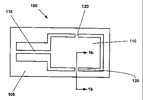
Referring initially to Figs. 1a and 1b, an embodiment of a micro machined
element 100 preferably includes a support structure 105, a mass 110, a
resilient
coupling 115, and one or more temporary bridges 120.
The support structure 105 is coupled to the resilient coupling 115 and the
temporary bridges 120. The support structure 105 is preferably adapted to
support
the resilient coupling 115 and the temporary bridges 120.
The mass 110 is coupled to the resilient coupling 115 and the temporary
bridges 120.
The resilient coupling 115 is coupled to the support structure 105 and the
mass 110. The resilient coupling 115 is preferably adapted to resiliently
support the
mass 110.
In a preferred embodiment, the mass 110 and resilient coupling 115 are
further adapted in a conventional manner to provide a spring-mass system for
use in
a conventional accelerometer.
8
CA 02384889 2002-03-12
WO 01/24228 PCT/US00/26355
The temporary bridges 120 are coupled to the support structure 105 and the
mass 110. The temporary bridges 120 are preferably adapted to temporarily
support the mass 110 until the temporary bridges 120 are severed during the
manufacturing process. In this manner, the temporary bridges 120 prevent
damage
to the resilient coupling 115 during the manufacturing process. In a preferred
embodiment, upon the conclusion of the manufacturing process, the temporary
bridges 120 are severed and the mass 110 is supported solely by the resilient
coupling 115.
In a preferred embodiment, as illustrated in Fig. 1b, the thickness of the
temporary bridge 120 is less than the thicknesses of the support structure 105
and
the mass 110. In a preferred embodiment, the thickness of the temporary bridge
120 is about 1 to 10% of the thickness of the thicknesses of the support
structure
105 and the mass 110. In a preferred embodiment, the thickness of the
temporary
bridge 120 is less than about 50 microns. In this manner, the structural
support of
the temporary bridge 120 is maximized while the force required to sever the
temporary bridge 120 in minimized. In an alternative embodiment, as
illustrated in
Fig. 1 c, the temporary bridge 120 includes one or more cavities 125 in order
to
further minimize the force required to sever the temporary bridge 120. In
another
alternative embodiment, as illustrated in Fig.1 d, the temporary bridge 120
includes
a tapered portion 130 having reduced width in order to further minimize the
force
required to sever the temporary bridge 120. In another alternative embodiment,
as
illustrated in Fig. le, the temporary bridge 120 includes a region 135 of
reduced
9
CA 02384889 2009-01-06
WO 01/24228 PCT/[JS00/26355
width in order to further minimize the force required to sever the temporary
bridge
120.
In a preferred embodiment, the micro machined element 100 is fabricated
from a silicon wafer using one or more of the merged-mask micro machining
processes disclosed in U.S. Patent No. 6,617,098 to Yu et al.
Referring to Figs. 2a and 2b, an altemative embodiment of a micro machined
element 200 preferably includes a support structure 205, a mass 210, resilient
couplings 215a and 215b and one or more temporary bridges 220.
The support structure 205 is coupled to the resilient coupling 215a and 21 5b
and the temporary bridges 120. The support structure 205 is preferably adapted
to
support the resilient couplings 215a and 215b and the temporary bridges 220.
The mass 210 is coupled to the resilient couplings 215a and 215b and the
temporary bridges 220.
The resilient couplings 215a and 215b are coupled to the support structure
205 and the mass 210. The resilient couplings 215a and 215b are preferably
adapted to resiliently support the mass 210. !n a preferred embodiment, the
resilient
couplings 215a and 215b are T-shaped resilient hinges.
In a preferred embodiment, the mass 210 and resilient couplings 215a and
215b are further adapted to provide a rotatina mirror for use in a bar code
scanning
system as disclosed in U.S. Patent No. 6,617,098 to Yu et al.
CA 02384889 2009-01-06
WO 01/24228 PCT/US00/26355
The temporary bridges 220 are coupled to the support structure 205 and the
mass 210. The temporary bridges 220 are preferably adapted to temporarily
support the mass 210 until the temporary bridges 220 are severed during the
manufacturing process. In this manner, the temporary bridges 220 prevent
damage
to the resilient couplings 215a and 215b during the manufacturing process. In
the
preferred embodiment, upon the conclusion of the manufacturing process, the
temporary bridges 220 are severed and the mass 210 is supported solely by the
resilient couplings 215a and 215b.
In a preferred embodiment, as illustrated in Fig. 2b, the thickness of the
temporary bridge 220 is less than the thickness of the support structure 205
and the
mass 210. In a preferred embodiment, the thickness of the temporary bridge 220
is
about I to 10% of the thickness of the thicknesses of the support structure
205 and
the mass 210. In a preferred embodiment, the thickness of the temporary bridge
220 is less than about 50 microns. In this manner, the structural support of
the
temporary bridge 220 is maximized while the force required to sever the
temporary
bridge 220 is minimized. In an altemative embodiment, as illustrated in Fig.
2c, the
temporary bridge 220 is tapered in order to further minimize the force
required to
sever the temporary bridge 220.
In a preferred embodiment, the micro machined element 200 is fabricated
from a silicon wafer using one or more of the merqed-mask micro machining
processes disclosed in U.S. Patent No. 6,617,098 to Yu et al.
11
CA 02384889 2009-01-06
WO 01124228 PCTIUSOUt26355
In a preferred embodiment, the micro machined element 200 is coupled to a
top cap and a bottom cap, as described in U.S. Patent No. 6,617,098 to Yu et
al.,
prior to severing the temporary bridge 220. In this manner, the mass 210 is
optimally
protected from shock and damage during the subsequent steps of the
manufacturing
process.
Referring to Fig. 3, a preferred embodiment of a method 300 for
manufacturing a micro machined structure having one or more temporary bridges
includes the steps of: (1) providing a top silicon wafer with an intemal layer
of silicon
dioxide and a bottom silicon wafer in step 305; (2) etching one or more
cavities in
the top surface of the bottom silicon wafer in step 310; (3) bonding the top
surface of
the top silicon wafer onto the bottom silicon wafer in step 315; (4) etching
the top
surface of the top silicon wafer in step 320; and (5) micro machining the top
surface
of the top silicon wafer to form a three dimensional structure including one
or more
temporary bridges in step 325.
As illustrated in Fig. 4a, in a preferred embodiment, in step 305, a top wafer
405 of silicon having an internal layer 410 of silicon dioxide and a bottom
wafer 415
of silicon are provided. In a preferred embodiment, the top wafer 405 of
silicon is a
silicon on insulator (SOI) wafer. In a preferred embodiment, the intemal layer
410 of
silicon dioxide is positioned about 5 to 50 microns above the bottom surface
of the
top wafer 405 of silicon.
12
CA 02384889 2002-03-12
WO 01/24228 PCT/US00/26355
As illustrated in Fig. 4b, in a preferred embodiment, in step 310, a cavity
420
is etched in the top surface of the bottom wafer 415 of silicon. The cavity
420 may
have any number of cross-sectional shapes. In a preferred embodiment, the
cavity
420 has a substantially rectangular cross-sectional shape.
As illustrated in Fig. 4c, in a preferred embodiment, in step 315, the top
wafer
405 of silicon is bonded onto the bottom wafer 415 of silicon. The top wafer
405
may be bonded to the bottom wafer 415 of silicon using any number of
conventional
processes for bonding wafers of silicon. In a preferred embodiment, the top
wafer
405 of silicon is bonded to the bottom wafer 415 of silicon using the process
of
silicon fusion bonding.
As illustrated in Figs. 4d and 4e, in a preferred embodiment, in step 320, the
exposed portions of the top wafer 405 and the internal layer 410 of silicon
dioxide
are etched. In a preferred embodiment, the exposed portions of the top wafer
405
and the internal layer 410 of silicon dioxide are etched using a conventional
KOH
etching process. In a preferred embodiment, the internal Iayer410 of silicon
dioxide
is used as an etch stop during the etching process. In a preferred embodiment,
the
thickness of the top wafer 405 after the etching process ranges from about 5
to 50
microns.
As illustrated in Fig. 4f, in a preferred embodiment, in step 325, a three
dimensional structure 425 is micro machined in the top wafer 405 of silicon
above
the cavity 420 in the bottom wafer 415 of silicon. In a preferred embodiment,
the
structure 425 is coupled to the remaining portions of the top wafer 405 of
silicon by
13
CA 02384889 2009-01-06
WO 01n4228 PCT/US00126355
one or more temporary bridges 430. In a preferred embodiment, as illustrated
in
Fig. 4g, the structure 425 is a strain gauge 435.
In a preferred embodiment, the structure 425 and the temporary bridges 430
are formed using one or more of the merged-mask micro machining processes
disclosed in U.S. Patent No. 6,617,098 to Yu et al.
In a preferred embodiment, the structure 425 is coupled to remaining portions
of the top wafer 405 of silicon by temporary bridges 430. The structure 425 is
then
preferabiy decoupled from the top wafer 405 of silicon by severing the
temporary
bridges 430. In this manner, the structure is protected from damage prior to
subsequent manufacturing operations. In a preferred embodiment, the temporary
bridges 430 are severed by removing the structure 425 from the top wafer 405
of
silicon using a conventional robotic arm. In an exemplary embodiment, the
structure
425 is a strain gauge 435 that is decoupled from the top wafer 405 of silicon
and
subsequently bonded to a substrate and wire bonded.
Referring to Fig. 5, an altemative preferred embodiment of a method 500 for
manufacturing a micro machined structure having one or more temporary bridges
includes the steps of: (1) providing a top silicon wafer with an intemal layer
of silicon
dioxide and a bottom silicon wafer in step 505; (2) etching one ore more
cavities in
the bottom surface of the top silicon wafer in step 510; (3) bonding the top
silicon
wafer onto the bottom silicon wafer in step 515; (4) etching the top surface
of the top
silicon wafer in step 520; and (5) micro machining the top surface of the top
silicon
14
CA 02384889 2002-03-12
WO 01/24228 PCTIUSOO/26355
wafer to form a three dimensional structure including one or more temporary
bridges
in step 525.
As illustrated in Fig. 6a, in a preferred embodiment, in step 505, a top wafer
605 of silicon having an internal layer 610 of silicon dioxide and a bottom
wafer 615
of silicon are provided. I n a preferred embodiment, the top wafer 605 of
silicon is an
SOI wafer. In a preferred embodiment, the internal layer 610 of silicon
dioxide is
positioned about 5 to 50 microns above the bottom surface of the top wafer 605
of
silicon.
As illustrated in Fig. 6b, in a preferred embodiment, in step 510, a cavity
620
is etched in the bottom surface of the top wafer 605 of silicon. The cavity
620 may
have any number of cross-sectional shapes. In a preferred embodiment, the
cavity
620 has a substantially rectangular cross-sectional shape.
As illustrated in Fig. 6c, in a preferred embodiment, in step 515, the top
wafer
605 of silicon is bonded onto the bottom wafer 615 of silicon. The top wafer
605 of
silicon may be bonded to the bottom wafer 615 of silicon using any number of
conventional processes for bonding wafers of silicon. In a preferred
embodiment,
the top wafer 605 of silicon is bonded to the bottom wafer 615 of silicon
using the
process of silicon fusion bonding.
As illustrated in Figs. 6d and 6e, in a preferred embodiment, in step 520, the
exposed portions of the top wafer 605 and the internal layer 610 of silicon
dioxide
are etched. In a preferred embodiment, the exposed portions of the top wafer
605
and the internal layer 610 of silicon dioxide are etched using a conventional
KOH
etching process. In a preferred embodiment, the internal Iayer610 of silicon
dioxide
CA 02384889 2009-01-06
= N
WO 01/24228 PCT/US00/26355
is used as an etch stop during the etching process. In a preferred embodiment,
the
thickness of the portion of the top wafer 605 of silicon above the cavity 620
after the
completion of the etching process ranges from about 5 to 50 microns.
As illustrated in Fig. 6f, in a preferred embodiment, in step 525, a three
dimensional structure 625 is micro machined in the top wafer 605 of silicon
above
the cavity 620 in the bottom surface of the top wafer 605 of silicon. In a
preferred
embodiment, the structure 625 is coupled to the remaining portions of the top
wafer
605 of silicon by one or more temporary bridges 630.
In a preferred embodiment, the structure 625 and the temporary bridges 630
are formed using one or more of the merged-mask micro machining processes
disclosed in U.S. Patent No. 6,617,098 to Yu et al.
In a preferred embodiment, the structure 625 is coupled to remaining portions
of the top wafer 605 of silicon by the temporary bridge 630. The structure 625
is
then preferably decoupled from the top wafer 605 of silicon by severing the
temporary bridges 630. In this manner, the structure 625 is protected from
damage
prior to subsequent manufacturing operations. In an exemplary embodiment, the
structure 625 is a strain gauge that is decoupled from the top wafer 605 of
silicon
and subsequently bonded to a substrate and wire bonded.
Referring to Fig. 7, an alternative preferred embodiment of a method 700 for
manufacturing a micro machined structure having one or more temporary bridges
includes the steps of: (1) providing a top silicon wafer and a bottom silicon
wafer in
16
CA 02384889 2002-03-12
WO 01/24228 PCT/US00/26355
step 705; (2) etching one or more cavities in the bottom surface of the top
silicon
wafer in step 710; (3) bonding the top silicon wafer onto the bottom silicon
wafer in
step 715; (4) etching the top surface of the top silicon wafer in step 720;
and (5)
micro machining the top surface of the top silicon wafer to form a three
dimensional
structure including one or more temporary bridges in step 725.
As illustrated in Fig 8a, in a preferred embodiment, in step 705, a top wafer
805 of silicon and a bottom wafer 810 of silicon are provided.
As illustrated in Fig. 8b, in a preferred embodiment, in step 710, a cavity
815
is etched in the bottom surface of the top wafer 805 of silicon. The cavity
815 may
have any number of cross-sectional shapes. In a preferred embodiment, the
cavity
815 has substantially rectangular cross-sectional shape.
As illustrated in Fig. 8c, in a preferred embodiment, in step 715, the top
wafer
805 of silicon is bonded onto the bottom wafer 810 of silicon. The top wafer
805 of
silicon may be bonded to the bottom wafer 810 of silicon using any number of
conventional processes for bonding wafers of silicon. In a preferred
embodiment,
the top wafer 805 of silicon is bonded to the bottom wafer 810 of silicon
using the
process of silicon fusion bonding.
As illustrated in Fig. 8d, in a preferred embodiment, in step 720, the exposed
portions of the top wafer 805 are etched. In a preferred embodiment, the
exposed
portions of the top wafer 805 of silicon are etched using a conventional wet
etching
process, dry etching process or a wafer polishing process. In a preferred
embodiment, the thickness of the top wafer 805 of silicon above the cavity 815
after
the completion of the etching process ranges from about 5 to 50 microns.
17
CA 02384889 2009-01-06
WO 01/24228 PCT/USOO/26355
As illustrated in Fig. 8e, in a preferred embodiment, in step 725, a three
dimensional structure 820 is micro machined in the top wafer 805 of silicon
above
the cavity 815 in the bottom surface of the top wafer 805 of silicon. In a
preferred
embodiment, the structure 820 is coupled to the remaining portions of the top
wafer
805 of silicon by one or more temporary bridges 825.
In a preferred embodiment, the structure 820 and the temporary bridges 825
are formed using one or more of the merged-mask micro machining processes
disclosed in U.S. Patent No. 6,617,098 to Yu et al.
In a preferred embodiment, the structure 820 is coupled to the remaining
portions of the top wafer 805 of silicon by the temporary bridges 825. The
structure
820 is then preferably decoupled from the top wafer 805 of silicon by severing
the
temporary bridges 825. In this manner, the structure 820 is protected from
damage
prior to subsequent manufacturing operations. In an exemplary embodiment, the
stnicture 820 is a strain gauge that is decoupled from the top wafer 805 of
silicon
and subsequently bonded to a substrate and wire bonded.
Referring to Fig. 9, an alternative preferred embodiment of a method 900 of
manufacturing a micro machined structure having one or more temporary bridges
includes the steps of: (1) providing a top silicon wafer and a bottom silicon
wafer in
step 905; (2) etching one or more cavities in the top surface of the bottom
silicon
wafer in step 910; (3) bonding the top silicon wafer onto the bottom silicon
wafer in
step 915; (4) etching the top surface of the top silicon in step 920; and (5)
micro
18
CA 02384889 2002-03-12
WO 01/24228 PCT/USOO/26355
machining the top surface of the top silicon wafer to form a three dimensional
structure including one or more temporary bridges in step 925.
As illustrated in Fig. 10a in a preferred embodiment, in step 905, atop wafer
1005 of silicon and a bottom wafer 1010 of silicon are provided.
As illustrated in Figs. 10b, in a preferred embodiment, in step 910, a cavity
1015 is etched in the top surface of the bottom wafer 1005 of silicon. The
cavity
1015 may have any number of cross-sectional shapes. In a preferred embodiment,
the cavity of 1015 has a substantially rectangular cross-sectional shape.
As illustrated in Fig. 10c, in a preferred embodiment, in step 915, the top
wafer 1005 of silicon is bonded onto the bottom wafer 1010 of silicon. The top
wafer
1005 of silicon may be bonded onto the bottom wafer 1010 of silicon using any
number of conventional processes for bonding wafers of silicon. In a preferred
embodiment, the top wafer 1005 of silicon is bonded to the bottom wafer 1010
of
silicon using the process of silicon fusion bonding.
As illustrated in Fig. 10d, in a preferred embodiment, in step 920, the
exposed portions of the top wafer 1005 are etched. In a preferred embodiment,
the
exposed portions of the top wafer 1005 of silicon are etched using a
conventional
wet etching process, dry etching process, or a wafer polishing process. In a
preferred embodiment, the thickness of the top wafer 1005 of silicon above the
cavity 1015 after the completion of the etching process ranges from about 5 to
50
microns.
As illustrated in Fig. 10e, in a preferred embodiment, in step 925, a three
dimensional structure 1020 is micro machined in the top wafer 1005 of silicon
above
19
CA 02384889 2009-01-06
= l
WO 01/24228 PCT/US00/26355
the cavity 1015 in the bottom surface of the top wafer 1005 of silicon. In a
preferred
embodiment, the structure 1020 is coupled to the remaining portions of the top
wafer
1005 of silicon by one or more temporary bridges 1025.
In a preferred embodiment, the structure 1020 and the temporary bridges
1025 are formed using one or more of the merged-mask micro machining processes
disclosed in U.S. Patent No. 6,617,098 to Yu et al.
In a preferred embodiment, the structure 1020 is coupled to the remaining
portions of the top wafer 1005 of silicon by the temporary bridges 1025. The
structure 1020 is then preferably decoupled from the top wafer 1005 of silicon
by
severing the temporary bridges 1025. In this manner, the structure 1020 is
protected from damage prior to subsequent manufacturing operations. In an
exemplary embodiment, the structure 1020 is a strain gauge that is decoupled
from
the top wafer 1005 and subsequently bonded to a substrate and wire bonded.
A micro machined apparatus has been described that includes a support
structure, one or more temporary bridges coupled to the support structure, and
a
mass coupled to the temporary bridge. In a preferred embodiment, the thickness
of
the temporary bridges are less than the thicknesses of the support structure
and the
mass. In a preferred embodiment, the thickness of the temporary bridges are
about
1 to 10% of the thickness of the support structure and the mass. In a
preferred
embodiment, the thickness of the temporary bridges range from about 5 to 50
microns. In a preferred embodiment, the temporary bridges include one or more
CA 02384889 2002-03-12
WO 01/24228 PCT/US00/26355
cavities. In a preferred embodiment, the apparatus further includes one or
more
resilient couplings coupled to the support and the mass. In a preferred
embodiment,
the resilient couplings are T-shaped hinges. In a preferred embodiment, the
support
structure, resilient couplings, and mass are an accelerometer. In an preferred
embodiment, the support structure, resilient couplings, and mass are a mirror
assembly. In a preferred embodiment, the mass is a strain gauge.
A method of manufacturing a micro machined apparatus also has been
described that includes micro machining a support structure coupled to a mass
using one or more temporary bridges in a substrate and severing the temporary
bridges. In a preferred embodiment, the mass is a strain gauge. In a preferred
embodiment, the method further includes micro machining one or more resilient
couplings in the substrate for coupling the mass to the support structure. In
a
preferred embodiment, the resilient couplings are T-shaped hinges.
A method of fabricating a micro machined structure also has been described
that includes providing a top silicon wafer and a bottom silicon wafer,
forming a
cavity in the bottom surface of the top silicon wafer, bonding the top silicon
wafer
onto the bottom silicon wafer, etching a portion of the top surface of the top
silicon
wafer and micro machining a three dimensional structure in the portion of the
top
silicon wafer above the cavity having one or more temporary bridges for
coupling the
three dimensional structure to the remaining portions of the top silicon
wafer. In a
preferred embodiment, the method further includes severing the temporary
bridges.
In a preferred embodiment, the three dimensional structure comprises a strain
gauge.
21
CA 02384889 2002-03-12
WO 01/24228 PCT/US00/26355
A method of fabricating a micro machined structure has also been described
that includes providing a top silicon wafer and a bottom silicon wafer,
forming a
cavity in the top surface of the bottom silicon wafer, bonding the top silicon
wafer on
to the bottom silicon wafer, etching a portion of the top surface of the top
silicon
wafer and micro machining a three dimensional structure in the portion of the
top
silicon wafer above the cavity having one or more temporary bridges for
coupling the
three dimensional structure to the remaining portions of the top silicon
wafer. In a
preferred embodiment, the method further includes severing the temporary
bridges.
In a preferred embodiment, the three dimensional structure comprises a strain
gauge.
A method of fabricating a micro machined structure also has been described
that includes providing as top silicon wafer having an internal layer of
silicon dioxide
and a bottom silicon wafer, forming a cavity in the bottom surface of the top
silicon
wafer, bonding the top silicon wafer, bonding the top silicon wafer onto the
bottom
silicon wafer, etching a portion of the top surface of the top surface of the
top silicon
wafer and micro machining a three dimensional structure in the portion of the
top
silicon wafer above the cavity having one or more temporary bridges for
coupling the
three dimensional structure to the remaining portions of the top silicon
wafer. In a
preferred embodiment, the method further includes severing the temporary
bridges.
In a preferred embodiment, the three dimensional structure is a strain gauge.
A method of fabricating a micro machined structure also has been described
that includes providing a top silicon wafer having an internal layer of
silicon dioxide
and a bottom silicon wafer, forming a cavity in the top surface of the bottom
silicon
22
CA 02384889 2002-03-12
WO 01/24228 PCT/US00/26355
wafer, bonding the top silicon wafer onto the bottom silicon wafer, etching a
portion
of the top surface of the top silicon wafer and micro machining a three
dimensional
structure in the portion of the top silicon wafer above the cavity having one
or more
temporary bridges for coupling the three dimensional structure to the
remaining
portions of the top silicon wafer. In a preferred embodiment, the method
further
includes severing the temporary bridges. In a preferred embodiment, the three
dimensional structure is a strain gauge.
A method of manufacturing a device including a micro machined structure
also has been described that includes temporarily coupling the micro machined
structure to a support structure using one or more temporary bridges,
decoupling the
micro machined structure form the support structure by severing the temporary
bridges and coupling the micro machined structure to a substrate.
A method of protecting a resilient coupling for coupling a mass to a support
structure also has been described that includes coupling the mass to the
support
structure using the resilient coupling and one or more temporary bridges and
severing the temporary bridges.
As will be recognized by persons of ordinary skill in the art having the
benefit
of the present disclosure, multiple variations and modifications can be made
in the
embodiments of the inventions. Although certain illustrative embodiments of
the
invention have been shown and described, a wide range of modifications,
changes,
and substitutions is contemplated in the foregoing disclosure. In some
instances,
some features of the present invention may be employed without a corresponding
use of the other features. Accordingly, it is appropriate that the foregoing
23
CA 02384889 2009-01-06
.. :
WO 01/24228 PCT/US00/26355
description be construed broadly and understood as being given by way of
illustration and example only, the scope of the invention being limited only
by the
appended claims.
24