Note: Descriptions are shown in the official language in which they were submitted.
APPL CRC 32.doc
CA 02385078 2002-03-15 Received 23 October 2001
1~.CURRECYEf~ ~E~SiO~!
1
A grating design
Field of the invention
The present invention relates broadly to a grating structure, method of
writing the
grating structure and devices incorporating such gratings. The present
invention will be
described herein with reference to grating structures for non-linear group
delay dispersion
compensation. However, it will be appreciated that the invention does have
broader
applications, such as for engineering of phase response of a fibre Bragg
grating device.
Background of the invention
Grating structures are widely used in optical waveguides for example as
filters or as
compensators for linear group delay dispersion.
In many systems non-linear group delay dispersion, i.e. second and higher
order group
delay dispersion, plays a significant role. Therefore, it is desirable that a
compensator structure
be provided that can compensate for non-linear group delay dispersion in such
systems.
Summary of the invention
The present invention provides an optical device incorporating a sampled
grating
structure having a chirped sampling period, wherein the grating structure is
arranged in a
manner such that, in use, a dispersion characteristic of the grating structure
is substantially
proportional to the inverse of a non-linear dispersion function over a
selected wavelength range.
The optical waveguide may be in the form of an optical fibre.
Alternatively, the optical waveguide may be in the form of a planar waveguide.
The present invention may alternatively be defined as a method of producing a
grating
structure in a photosensitive optical waveguide, the method comprising the
step of irradiating
the device with UV light at an intensity sufficient to induce refractive index
variations in the
waveguide in a manner to produce a sampled grating structure, wherein the
radiation is
controlled in a manner to effect chirping of the sampling period, and such
that a dispersion
characteristic of the grating structure is substantially proportional to the
inverse on a non-linear
dispersion function over a selected wavelength range.
AMENDED ~~~:~ ~
'PEAII~t~
APPL_,!.r_ ~_s2.doc PCT/AU00/01151
CA 02385078 2002-03-15 Received OS December 2001
CORREG~'EC~ ~'ERSI~~
2
The method may further comprise a step of applying an apodisation function
during the
UV-inducing of the refractive index variations to produce a smooth grating
profile. This can
help to avoid ripples.
The photosensitive optical waveguide may comprise an optical fibre or planar
optical
waveguide.
The invention further provides an optical waveguide incorporating a sampled
grating
structure a having chirped sampling period, wherein the grating structure is
arranged in a
manner such that, in use, a dispersion characteristic of the grating structure
is substantially
proportional to the inverse of a non-linear dispersion fi~nction over a
selected wavelength range.
The invention may alternatively be defined as a method of compensating for non-
linear
group delay dispersion in an optical signal, comprising transmitting the
optical signal through a
sampled grating structure having a chirped sampling period.
The invention may alternatively be defined as providing a group delay
dispersion
compensator device comprising a sampled grating structure a having chirped
sampling period,
wherein the grating structure is arranged in a manner such that, in use, a
dispersion
characteristic of the grating structure is substantially proportional to the
inverse of a non-linear
dispersion function over a selected wavelength range.
Having made this invention, it has been recognised that a method of producing
a zero
dispersion WDM channel can be provided, the method comprising the steps of
- filtering a narrow band optical signal from an input broad band optical
signal using a
square reflection band filter;
- using a sampled grating structure having a chirped sampling period to
compensate for
dispersion of the narrow band optical signal in the reflection band filter.
It is noted here that the terms "narrow band" and "broad band" are not
intended to be
limited to a particular range, but rather to indicate the relative breadth of
one when compared
with the other.
Further, the present invention provides a device for producing a zero
dispersion WDM
channel, the device
,:~~i.:...' . . ' 'lihc~'~.
CA 02385078 2002-03-15
WO 01/22126 PCT/AU00/01151
- 3 -
comprising a square reflection band filter for filtering a
narrow band optical signal from an input broad band optical
signal, and following the optical filter, a sampled grating
structure having a chirped sampling period for compensating
for dispersion of the narrow band optical signal in the
square reflection band filter.
The device may comprise a circulator having a
plurality of ports, the square reflection band filter being
located at one of the ports for filtering the square
amplitude narrow band optical signal from the input broad
band optical signal entering the circulator at an input
port, and the sampled grating structure being located at
another port of the circulator to compensate for dispersion
in the square band filter, the circulator further
comprising an output port for outputting the dispersion-
compensated narrow band optical signal.
The invention has applications for both planar and
cylindrical waveguides such as optical fibres.
Preferred forms of the invention will now be
described, by way of example only, with reference to the
accompanying drawings, in which:
Brief Description of the Drawings
Figure 1A shows a typical refractive index profile of
a grating produced by W-induced refractive index
variations.
Figure 1B shows a portion of the profile shown in Fig.
1A on an expanded length scale to more clearly show the
refractive index variations in the grating.
Figure 2 is a schematic drawing illustrating direct W
writing techniques.
Figure 3 is a schematic drawing illustrating
interferometric W writing techniques.
Figure 4A shows a refractive index profile of a
sampled grating.
CA 02385078 2002-03-15
WO 01/22126 PCT/AU00/01151
- 4 -
Figure 4B shows a portion of the profile shown in Fig.
4A on an expanded length scale to more clearly show the
refractive index variations in the grating.
Figure 5A shows a refractive index profile of a
grating embodying the present invention.
Figure 5B shows a portion of the profile shown in Fig.
5A on an expanded length scale to more clearly show the
refractive index variations in the grating.
Figure 6 is a plot illustrating group delay dispersion
of an apodised grating embodying the present invention.
Figure 7A shows an apodised refractive index profile
of a grating embodying the present invention.
Figure 7B shows a portion of the profile shown in Fig.
7A on an expanded length scale to more clearly show the
refractive index variations in the grating.
Figure 8 shows a plot illustrating group delay
dispersion of a WDM channel.
Figure 9 is a schematic drawing of an optical device
embodying the present invention.
Figure 10 shows a plot illustrating the resulting
group delay dispersion of the optical device of Figure 9.
Detailed Description of the Preferred Embodiments
In Figures 1A and 1B, a typical refractive index
profile 10 of a grating produced by W-induced refractive
index variations in a photosensitive waveguide material is
shown. The profile is substantially sinusoidal, with a
spatial period A. For Bragg gratings, typical spatial
periods will be of the order of parts of micrometers such
that the Bragg condition is fulfilled for a particular
wavelength. Typically, the wavelengths of optical signals
utilised in optical devices are between 1200 and 1600 nm.
The refractive index profile 10 is achieved by
utilising interference of UV light beams for W-inducing
the refractive index variations in a photosensitive
CA 02385078 2002-03-15
WO 01/22126 PCT/AU00/01151
- 5 -
material, either through direct writing techniques (see
Figure 2) or interferometric techniques (see Figure 3).
In sampled gratings the amplitude of the refractive
index variation (e. g. sinusoidal variation) is varied
periodically, resulting in a refractive index profile 40 as
illustrated in Figures 4A and 4B. A typical sampling
period length would be of the order of millimeters.
From the above it follows that whilst the spatial
period of the grating, which is typically of the order of
parts of micrometers, is a parameter which is
experimentally difficult to control and/or manipulate, the
sampling spatial period is experimentally relatively easy
to control and/or manipulate.
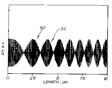
As illustrated in Figures 5A and 5B, the refractive
index profile 50 of a sampled grating for which the
sampling period has been chirped, the spatial period of the
sinusoidal "envelope" 52 due to the sampling function
decreases along the length of the grating. Importantly,
the period of the grating AZ remains constant throughout
the entire length of the grating, thereby placing no
special demands on the writing of the short period
structure. Only the relatively "long" period of the
sampling function needs to be varied.
It is noted here that for illustrative purposes the
sampling period lengths of Figures 5A and 5B have been set
to higher values as they would typically be in a real
system.
In Figure 6, the group delay dispersion 60 of an
example sampled grating written with a chirped sampling
period is shown. The sampling function is:
~cos~(Ko + OK(z))z~ + cos((Ko - OK(z))z~~ l 2 = cos~Koz~ cos~OK(z)z~ .
Furthermore, an apodisation function has been applied
in the form of a function which monotonically decreases
from a starting value at the beginning of the grating to
zero at the end of the grating. The refractive index
CA 02385078 2002-03-15
WO 01/22126 PCT/AU00/01151
- 6 -
profile 62 of the resulting grating is shown in Figures 7A
and 7B.
It will be appreciated that the group delay dispersion
shown in Figure 6 can be utilised to compensate for non-
linear group delay dispersion, for example for non-linear
group delay dispersion in a WDM channel.
In Figure 8, the group delay dispersion 80 of a WDM
channel is illustrated. The group delay dispersion is
substantially inverse to the group delay dispersion 60 of
the example grating structure (see Figure 6) and it will be
appreciated by a person skilled in the art that through
appropriate selection of the sampling function and
apodisation function, group delay dispersion in WDM
channels can be compensated using a sampled grating for
which the sampling period has been chirped.
In Figure 9, an optical device 90 comprises a
circulator 92 having a sampled grating structure 91 with a
chirped sampling period at one port 94 and a grating filter
96 optimised for "square" reflection band amplitude
response at another port 98. An incoming broad band
optical signal 100 entering the circulator at an input port
102 will initially propagate to the grating filter 96, of
which a narrow band signal (not shown) within the square
reflection band is reflected back into the circulator 92.
The narrow band signal is then reflected at the sampled
grating 91 having the chirped sampling period, whereby an
output signal 106 leaving the circulator 92 at an output
port 108 will be a narrow band optical signal with
substantially zero group delay dispersion within the
square-shaped amplitude "channel". In other words, the
group delay is substantially constant within the square-
shaped amplitude channel, as shown in Figure 10, portion
110 of graph 112.
It will be appreciated by a person skilled in the art
that numerous variations and/or modifications may be made
to the present invention as shown in the specific
CA 02385078 2002-03-15
WO 01/22126 PCT/AU00/01151
_ 7 _
embodiments without departing from the spirit or scope of
the invention as broadly described. The present
embodiments are, therefore, to be considered in all
respects to be illustrative and not restrictive.
For example, apodisation functions other than the one
described could be used during the writing of the sampled
grating with a chirped sampling period.