Note: Descriptions are shown in the official language in which they were submitted.
CA 02385430 2002-05-08
CONTROL ARRANGEME:NT AND ISOLATED POWER SUPPLIES
FOR POWER ELECTRONIC SYSTEM
BACKGROUND OF THE INVENTION
1. Field of the Invention
The present invention relates generally to the field of power electronic
systems
and more particularly to control methods and arrangements that monitor the
condition
and operating parameters of the power electronic system and power electronic
switches
and provide appropriate action to optimize operation thereof.
2. Description of Related Art
In high-voltage power electronic switches, several switch devices must be
connected in series, e.g. as a stack of series-connected power electronic
device
modules or stages as shown in U.S. Patent Nos. 6,333,853. To control and
provide
diagnostics for each individual switch device, an isolated power supply must
be
provided at the potential of each switch device. This requires that the power
supply be
adequately insulated from both ground potential and adjacent stages or
modules.
Ttiese insulation requirements require that any transformer that is used to
provide the
power supply and that is connected between ground and the full line potential
of the
power electronic switch be rather large and costly.
Additionally, prior art arrangements do not provide appropriate diagnostics or
system control with sufficient emphasis on the priority of the continuous
supply of the
connected load.
SUMMARY OF THE INVENTION
Accordingly it is a principal object of the present invention to provide a
control
method and arrangement that monitors the condition and operating parameters of
a
power electronic system having power electronic devices.
It is another object of the present invention to provide electrically isolated
power
supplies to individual control stages fior high-voltage, series-connected
switch
devices/power electronic devices.
These and other objects of the present invention are efficiently achieved by a
control method and arrangement thai: monitors the condition and operating
parameters
of a power electronic system having power electronic devices to optimize
operation of
CA 02385430 2002-05-08
the power electronic system. Further, electrically isolated power supplies to
individual
control stages for high-voltage, series-connected switch devices/power
electronic
devices.
BRIEF DESCRIPTION OF THE DRAWING
The invention, both as to its organization and method of operation, together
with
further objects and advantages thereof, will best be understood by reference
to the
specification taken in conjunction with the accompanying drawing in which:
FIG. 1 is a block diagram representation of a power electronic system
utilizing
the control arrangement of the present invention;
FIGS. 2-8 are diagrammatic representations of signals at various points in the
system of FIG. 1;
FIG. 9 is a one-line, block diagram representation of a power electronics
svvitching system utilizing the control arrangement of the present invention;
FIG. 10 is a one-line, diagrammatic representation of portions of a solid-
state
svritch of FIG. 9; and
FIGS. 11 and 12 are block and schematic diagrams of a power supply
arrangement for portions of the power electronic system of FIG. 1.
DETAILED DESCRIPTION
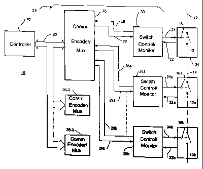
Referring now to FIG. 1, the control arrangement and method of the present
invention will be described in connection with an illustrative system 15 that
includes a
controller 18 that monitors the condition and operating parameters of various
components of the system 15 and takes appropriate action to optimize operation
thereof, e.g. the operating characteristics of an illustrative electronic
switch stage 10 are
monitored as will be explained in moi-e detail hereafter. As illustrated, the
electronic
switch stage 10 includes a main path between lines 12 and 14 that is
controlled
between on and off states, corresporiding to respective conductive and non-
conductive
states, via a control connection at 16. In a specific illustrative example,
the electronic
switch stage 10 is a thyristor, IGBT, TRIAC, pair of inverse-parallel
connected SCR's, or
other actively controlled device.
The system 15 includes an illustrative communications arrangement 22 that
cooperates with the controller 18 to provide information to the controller 18
over
communications lines at 20, which in specific embodiments is formed by one or
more
-2-
CA 02385430 2002-05-08
data buses and/or control lines. In the illustrative embodiment, the
communications
arrangement 22 includes a switch control/monitor stage 30 that is located in
the vicinity
of the system component to be moriitored, e.g. the electronic switch stage 10,
and that
transmits monitored information to a communications encoder/multiplexer stage
26,
"comm. encoder/mux" 26 hereafter, via a communications link 28, e.g. a
dielectric
niedium such as fiber optics in a specific embodiment. As illustrated, where
multiple
components are monitored by the system 15, multiple switch control/monitor
stages 30
are provided along with multiple communication links 28, e.g. 28a, 28b. The
comm.
encoder/mux stage 26 then functions to multiplex the information on the
various
communication links 28 and provides the information in a predetermined
multiplexed
format at 20 to the controller 18.
The control connection 16 of the electronic switch stage 10 is connected to a
gate drive signal at 24 provided by the switch control/monitor stage 30. In
this
ilVustrative example, the system 15 rnonitors the gate drive signal at 24
and/or the
temperature of the switch stage 10 via data at 32. This arrangement is
especially
useful where the illustrative electronic switch stage 10 or various other
component is
located remotely from the controller 18 and/or where the illustrative
electronic switch
stage 10 is located in a more severe environment that is deleterious for the
controller
18, e.g. high-noise, medium voltage, high-temperature etc. In one specific
embodiment, the temperature of the switch stage 10 is measured at the location
of the
switch control/monitor stage 30 with the switch control/monitor stage 30 being
in the
proximate vicinity of the switch stage 10, e.g. on a common mounting
arrangement or
heat sink 34 (not shown in detail).
Considering now an illustrative embodiment of the communications arrangement
2:2 of the system 15 and referring nciw additionally to FIG. 2, the
information on the
communication link 28 includes a representation of the gate drive signal 24,
such that a
pulse signal 40 is sent over the communications link 28 when the electronic
switch
stage 10 is conducting. The pulse signal 40 is sent on a repetitive basis,
e.g. each
basic clock cycle or each half-cycle of a fundamental waveform that is present
on the
lirie 12 to the electronic switch stage 10. The receipt of this signal 40 by
the comm.
encoder/mux stage 26 and the transmission of this representation to the
controller 18
over lines 20 also indicates that the communications arrangement 22 is
operational and
that the electronic switch stage 10 is not shorted.
-3-
CA 02385430 2002-05-08
In the illustrative embodiment of FIG. 1, the electronic switch stage 10 is
one
stage of an overall series-connectecl electronic switch, e.g. six stages as
depicted in
FIG. 1 by a second stage 10a and a sixth stage 10b. Also provided for each
stage is
one of the switch control/monitor stages 30, e.g. 30, 30a, 30b which transmits
a signal
on each of the communication links 28, e.g. 28, 28a and 28b, to the comm.
encoder/mux stage 26. For example, as depicted in FIG. 2, respective signals
42 and
44 are transmitted for the second and sixth electronic switch stages 10a and
10b which
ai-e generated simultaneously and repetitively. The comm. encoder/mux stage 26
then
miultiplexes the received pulse signals, e.g. 40, 42 and 44, and provides the
multiplexed
signal at lines 20 to the controller 18. Accordingly, the receipt by the
controller 18 of the
continuous train of pulses verifies that each switch stage of the stages 10,
10a, 10b
etc., denoted as lOx hereafter, is conducting. If the pulses are not
continuous, e.g. not
present in the predetermined patterri and spacing as shown in FIG. 3, i.e. one
or more
of the pulses are missing at the periodic rate, then the controller 18 is
advised/alerted
that something is wrong with either one of the electronic switch stages 10x or
the
communication arrangement 22. If the pulse train of multiplexed signals at 20
is
synchronized to the controller 18, the controller 18 can identify which of the
stages has
a malfunction, e.g. stage 3 in FIG. 3 as indicated by the missing pulse
denoted 62.
Considering now an illustrative embociiment where additional information is
transmitted over the communications arrangement 22 and referring now
additionally to
FIG. 4, it is desirable for the controller 18 to ascertain additional
information about the
various components of the system 15, e.g. the temperature of the electronic
switch via
the sensed temperature signal 32. To accomplish the communication of
additional
information, the switch control/monitor stage 30 encodes additional
information along
with the gate driver signal information, e.g. as shown in FIG. 4 by the
addition of a pulse
signal 50 that represents temperature of the electronic switch stage 10 along
with a
representation of the gate driver signal, e.g. pulse signal 52. In a specific
arrangement,
the width of the pulse 50 is proportional to the sensed temperature at 32.
Thus, the
pulse signals 50, 52 are sent over the communications link 28 on a periodic
basis, e.g.
as discussed before, for each basic operational cycle of the system 15. For
example,
pulse signals 50, 52 correspond to a switch control/monitor stage 30
associated with a
first electronic switch stage 10 and pulse signals 54, 56 correspond to the
stage 30a
associated with a second electronic switch stage 10a. It should be noted that
in FIG. 4,
while the pulses are shown sequentially for each stage, the pulses for each of
the
-4-
CA 02385430 2002-05-08
stages is sent repetitively and simultaneously, the representation in FIG. 4
being the
n-iultiplexed sequential arrangement performed by the comm. encoder/mux stage
26 in
response to the continuous information received from the various stages on the
communication links 28, 28a, 28b etc.
In a specific embodiment, the comm. encoder/mux stage 26 also incorporates an
ai-nbient temperature signal to the controller 18. For example, with
additional reference
to FIG. 5, after the comm. encoder/rnux stage 26 outputs a sequence of pulses
corresponding to each of the stages, an ambient temperature signal 60 is
encoded or
multiplexed into the pulse train in place of the first stage signal or other
position. Thus,
the controller 18 receives a pulse train of signals representing the gate
signal and the
temperature of each of the switch stages 10x followed by the ambient
temperature of
the environment of the controller 18 and the comm. encoder/mux stage 26. In
this
manner, the temperature rise of eaclh switch stage 10 above the ambient
temperature is
available. Additionally, as shown in FIG. 5, the absence of a pulse signal for
any of the
stages, e.g. at 63 for stage 3, indicates a malfunction of the communications
link or the
gate drive signals or the shorted condition of the respective switch stage 10
etc.
In accordance with additional aspects of the present invention, and referring
now
aciditionally to FIG. 6, in a preferred embodiment, the gate driver signal
pulse 40 is
transmitted over the communications link 28, on a normal basis in one specific
ernbodiment, or in another specific embodiment, upon a requested basis as
determined
by the controller 18. For example, the controller 18 issues a request signal,
as
illustrated at 64 in FIG. 6, on a communications line 29, e.g. a dielectric
medium such
as fiber optics in a specific embodiment, to instruct/condition the switch
control/monitor
stage 30 to initiate the transmission of the combined additional information
of the gate
signal and the temperature of the switch stage 10. Thus, the stage 30 sends
the
normal signals as shown in FIG. 2 uritil a request signal is received
whereupon the
signals depicted in FIG. 4 are sent, all as depicted in the sequence of FIG.
6.
In accordance with additional aspects of the present invention, the controller
18
over the communication lines at 20 is; arranged to issue predetermined ON or
OFF
signals to control the conductive state of the switch stages 10 to 10b over
the
communications link 29 of the communications arrangement 22. In response to
the ON
or OFF signals at 20, the switch control/monitor stage 30 sends a gate drive
control
siginal at 24 to turn the switch on or off in accordance with the received
signal. For
example, signals at 20, either on one line or as a coded representation, are
responded
-5-
CA 02385430 2002-05-08
tc- by the comm. encoder/mux stage 26 which issues an ON signal representation
over
the communications link 29 to the switch control/monitor stage 30. The switch
control/monitor stage 30 decodes the ON signal representation on the
communications
lirik 29 and outputs a signal at 24 to the switch stage 10. In one embodiment,
a
rriomentary ON signal at 20 causes the stage 30 to turn the switch stage 10 on
and the
switch stage 10 is turned off only upon the issuance of a momentary OFF signal
at 20.
In another embodiment, the ON sigrial is continuously output at 29 until the
switch
control/monitor stage 30 responds with one or more predetermined signals over
the
communication link 28 to acknowledge that the ON signal has been received and
acted
upon and/or that the switch stage 1 C- is conducting, e.g. as shown at 65 or
66 in FIG. 5.
In a specific embodiment, the ON/OFF signals at 20 are encoded over the
communications link 29 as a pulse tr=ain of a predetermined number of pulses,
the ON
and OFF signals being a different number of pulses. The comm. encoder/mux
stage 26
ericodes the pulse train and the switch control/monitor stage 30 counts the
pulses of
the signal and determines whether or not the received signal is an ON or OFF
signal.
In one embodiment, the request for diagnostic signal issued by the comm.
encoder/mux
stage 26 at 29 is a third signal, e.g. a different number of pulses than the
ON or OFF
signal representations In another embodiment, the request for diagnostic
signal to start
the transmission of temperature signals over the communication link 28 is the
transmission of a predetermined "ON" signal over the link 29. Considering
another
illustrative embodiment of the preserit invention and referring now
additionally to FIG. 7,
the temperature signal alone is comrnunicated via the communications
arrangement 22
of FIG. 1, e.g. signal 50 for stage 10, 54 for stage 10a, and the signal 60
for ambient
ternperature at the stage 26. In another embodiment, a distinct ready signal
is utilized
by the comm. encoder/mux stage 26 to ready the switch stages 10x for operation
in
response to an ON command being i-eceived from the controller 18 when the
switch
stages lOx are non-conducting. In such cases, the switch control/monitor
stages 30
respond to the detection of the distinct ready signal, e.g. predetermined
number of
pulses at 29, by sending a signal such as 40 in FIG. 1or 65 or 66 of FIG. 5
over the
communications link 28. When the signals are received by the comm. encoder/mux
stage 26, it can be determined that the switch stages 10x are ready for
operation and
ON signals can be issued over the communication links 29.
The system 15 in a preferred embodiment is applied to a multi-phase electrical
power distribution system operating at medium voltages. Accordingly, as shown
in FIG.
-6-
CA 02385430 2002-05-08
1, the system 15 includes additional comm. encoder/mux stages 26, e.g. 26-2
and 26-3
for respective second and third phases of an electrical power source. In one
ernbodiment, the stages 26, 26-2 and 26-3 are connected to receive signals
from the
controller 18 over a common data bus 20 while in other embodiments the
signaling
paths are independent. In such systems, when the power electronic switch of
stages
10, 10a, 10b etc. is non-conducting, it may be desirable to verify its
readiness for
operation, especially when it may be called upon for rapid, high-speed
operation in a
high-speed source-transfer application. In one embodiment, and referring now
to FIG.
8, when the comm. encoder/mux stage 26 receives a signal at 20 from the
controller 18
representing that the switch stages 10x are to be tested, the comm.
encoder/mux stage
26 issues ON commands to a first portion of the switch control/monitor stages
30, e.g.
N/2 where there are N total switch stages 10x, or (N+1)/2 where N is an odd
number,
and thereafter issue ON commands to the remaining switch control/monitor
stages 30.
Accordingly, the information represeriting operation of the various switch
stages 10x is
provided to the controller 18 as shown in FIG. 8, first for the first three
stages then for
the next three stages. This is useful because a non-conducting switch can be
tested
while the overall switch remains non-conducting. Additionally, in a preferred
enibodiment, the ambient temperature is also provided, as shown at 60 in FIG.
8. As
before, in various embodiments, this can be done with the temperature
representations
for each stage as shown in FIG. 8 or without the individual temperature
representation
signals.
Referring now to FIG. 9, a power electronic switching system functioning as a
high-speed source transfer switching system (HSSTSS) 110 is illustrative of a
specific
system application for which the control arrangement and method of the present
invention of FIGS. 1-8 is useful. The HSSTSS 110 supplies a load at 114 with
an
alternating-current waveform via either a first AC source at 116 or a second
AC source
at 118. The first and second AC sources 116 and 118 and the load at 114 as
provided
in an electrical power distribution syst:em are typically multi-phase circuits
which are
represented in FIG. 9 by a one-line diagram. The HSSTSS 110 includes a first
solid-
state switch, SSS1, 120 and a second solid-state switch, SSS2, 122, which can
also be
characterized as electronic switches or power electronic switches. The HSSTSS
110
via a system control 112 controls either SSS1 to supply the load at 114 via
the first
source 116 or controls SSS2 to supply the load at 114 via the second source
118. In a
specific embodiment, the system control 112 includes the controller 18 of FIG.
1. The
-7-
CA 02385430 2002-05-08
system control 112 provides appropriate control signals at 128, 130 to control
the
operation of each respective solid-state switch, SSS1 120 and SSS2 122. In the
specific illustrative embodiment, the system of FIG. 9 utilizes the
communications
arrangement 22 of FIG. 1. Accordirigly, the control signals at 128, 130 are
utilized by
the communications arrangements 22-1 and 22-2 to control the respective solid-
state
switches SSS1 120 and SSS2 122 over respective gate drive signal arrangements
24-1
and 24-2.
In operation, the system control 112 samples the voltage waveforms of each
source 116, 118, e.g. via respective sensing inputs at 124, 126 to detect when
transfer
between the sources is desirable, e.g. sensing outages and momentary
interruptions as
well as voltage sags and swells based on the source supplying the load being
above or
below preset levels. For example, assume that SSS1 120 is turned on by the
system
control 112 via signals at 128 so as to be conductive and supply the load at
114. If the
system control 112 via the sensing input 124 senses that the voltage of the
first source
at 116 is exhibiting undesirable characteristics, the system control 112 via
the control
signals at 128, 130 turns off SSS1 and turns on SSS2 so as to transfer the
supply of
the load at 114 from the first source at 116 to the second source at 118. As
used
herein, the term "incoming" is used to describe the source and the SSS that
will be
turned on to supply the load (e.g. the second source at 118 and SSS2 in the
illustrative
example), and the term "outgoing" is used to describe the source and the SSS
that is
being turned off (e.g. the first source at 116 and SSS1 in the illustrative
example).
Referring now to FIG. 10, each of the solid-state switches SSS1 and SSS2
includes one or more arrays of inverse parallel connected thyristors, e.g.
140a and
140b for SSS1 and 142a and 142b fi:)r SSS2. In illustrative implementations,
each array
of thyristors is rated in the range of 2-12 kv. To provide operation in medium
voltage
systems, e.g. operating in the range of 2-34.5 kv, one or more of such
thyristors SSS1
and SSS2 are connected in series for each phase of the sources, e.g. a
plurality of
such thyristors being referred to as a stack. Thus, while the term thyristor
is used for
the solid-state switches SSS1, 140 and SSS2, 142, in specific implementations
at
medium voltages, this commonly refers to a thyristor stack. For example, in a
specific
erribodiment, each of the solid-state switches SSS1 and SSS2 is implemented by
a
piurality of the switch stages 10x of FIG. 1.
Considering now operation of the control arrangement and method of the
present invention, transfer of the load at 114 from one source to the other,
e.g. the first
-8-
CA 02385430 2002-05-08
source at 116 to the second source at 118, is generally accomplished by
removing the
gating signals at 128a, 128b to shut off SSS1 and starting the gating signals
at 130a,
130b to turn on SSS2. Thus, the first source at 116 ceases to supply the load
at 114
aind the second source at 118 begins to supply the load at 114. For desirable
transfer
control, the controller 112 is provided with additional sensing inputs, e.g.
the incoming
source-voltage differential is determined by the load voltage at 114 as sensed
via a
sensing input 127 or by the differential of the source voltages sensed at 124,
126, and
the current to SSS1 and SSS2 being sensed via respective current sensing
inputs at
1;29 and 131.
In accordance with additional aspects of the present invention, the system
control 112 is provided with features to respond to an overheated condition of
the solid
state switches SSS1 and SSS2 to transfer the load at 114 to the alternate
source. For
example, if the temperature sensed via either the communications arrangement
22, or a
separate temperature sense line 150 in a specific embodiment, indicates an
overheated
condition, the system control 112 proceeds with a high-speed transfer. The
system
control 112 then denotes the alternate source as the preferred source. The now
denoted alternate source with the overheated switch is still available on a
temporary
basis for transfers when the system control 112 detects voltage disturbances
on the.
source currently feeding the load such that transfer is required. In an
illustrative
ernbodiment, the overheated condition is defined by any stage of a solid-state
switch
SSS having a sensed temperature ttiat exceeds the ambient temperature by a
predetermined differential. i.e. temperature rise. For example, with reference
to FIG. 1,
if any electronic switch stage 10 has a sensed temperature at 32 that exceeds
the
predetermined limits, an overheated condition is determined.
When an overheated condition is detected, if it is not possible to transfer to
ariother viable source, the system 110 includes additional features to
initiate and
accomplish a backup transfer to bypass and isolate the switches SSS1 and SSS2
of
the system 110. Specifically, in an illustrative embodiment, as shown in FIG.
9, to
accomplish a bypass/isolation sequence, the system controller 112 controls two
bypass
switches BP-1 and BP-2 and two isolation switches 1-1 and 1-2. The switches BP-
1, BP-
2, I-1 and 1-2 are controlled via respective control lines 160, 162, 164 and
166. In
accordance with additional features of the present invention, the
bypass/isolation
sequence is performed to assure optimum load continuity, e.g. as described by
the
following steps:
-9-
CA 02385430 2002-05-08
Disable high speed transfer control (maintain SSS1, SSS2 states);
Close bypass switch(es) (e.g. BP-1) to match the presently conducting SSS('s),
e.g. SSSI;
Confirm that the appropriate bypass switches respond;
Open all isolation switches (e.g. I-1, 1-2);
Confirm that the appropriate isolation switches respond;
Remove all gating signals (e.g. at 128, 130) from all SSS's
Enable backup transfer contrcd (e.g. in this case because an SSS is deemed
uriusable)
In situations where backup transfer control is enabled, e.g. to perform
maintenance or service, an overheated SSS, or otherwise unusable SSS (e.g. due
to
lack of control), the system control 1'12 is capable of providing source
transfer control
using the bypass switches BP-1, BP-2, with the isolation switches I-1, 1-2
remaining
open.
In accordance with additional features of the present invention, when
diagnostic
information is received by the system controller 112 indicating a potential
shorted
condition of a switch SSS, e.g. as detected by the loss of the gating signal
40 or 52 for
a particular switch stage 10x in FIGS. 1-8, the system controller 112 will
identify the
switch SSS and the location of the stage within the switch of the potential
problem.
Appropriate flags, alarms etc. are set and issued. However, the system 110
will
continue to operate normally and be fully functional since the switches SSS
are
designed with devices having suitablE: predetermined ratings sufficient to be
able to
furiction when one of the switch stages lOx is shorted. If diagnostic
information is
received that identifies a potential shorted condition of a second of the
switch stages
10x within the same phase or pole of a switch SSS, the system controller 112
initiates
the backup transfer mode as discussed hereinbefore and the high-speed transfer
function is disabled. As discussed hereinbefore in connection with diagnostics
of the
-10-
CA 02385430 2002-05-08
operating parameters of the switches such as SSS1 of the system 110 and the
switch
stages 10x of FIG. 1, the loss of the signals 40 or 52 indicates that either
the switch
stage 10x is shorted, the communications arrangement 22 is not functioning or
the gate
di-ive signals at 24 are not functioning.
Considering yet further additional features of the present invention, the
system
controller 112 also monitors the voltage across each switch SSS that is
supposed to be
in a conducting mode, i.e. the switch SSS that is supplying the load at 114.
For
example, the system controller 112 rnonitors the differential voltage between
116 and
114 for switch SSS1. If the differentiial voltage is greater than a
predetermined value,
e.g. 1500v for a 15kV system, the system controller 112 concludes that the
there is a
malfunction. This detected condition could be caused by an isolation switch
being open
(which would not be normal), a blown fuse in the circuit, or the discontinuity
of the
svvitch SSS1 (i.e. non-conducting status such as caused by an open circuit or
broken
connection). If this condition is detected and persists for a predetermined
time interval,
e.g. 2 milliseconds, the system contrDller 112 initiates a transfer to the
second source
118 by turning on the switch SSS2, and also locks out any transfer back to the
switch
SSS1. Of course, if for any reason an alternate viable source is not
available, the
system controller initiates a backup transfer as discussed hereinbefore. In
addition or
as an alternative to the diagnostic testing of non-conducting switches as
discussed
hereinbefore, if a switch SSS1 has not been turned on in a,predetermined
period of
tirrie, e.g. one day, the system controller 112 initiates a transfer to
interrogate the switch
SSS1 to verify proper operation to ensure that a viable alternate source is
available if
needed.
Considering now additional aspects of the present invention to provide
electrically isolated power supplies to individual control stages for medium
and high-
voltage, series-connected switch devices/power electronic devices and
referring now to
FIG. 11, a stack of series-connected power electronic switch devices 82a-d and
84a-d,
e.g. SCR's arranged in so-called inverse parallel connection, illustrate a
typical
arrangement to provide one phase of a power electronic switch, although the
number of
switch devices SCR's 82, 84 is variable and depends on the voltages involved
in the
application and the rating of the switch devices. Associated with the switch
devices 82,
84 are respective mounting and interconnection bus structure referred to
generally at
80, e.g. 80a-80d. To provide individual control and diagnostics for the switch
devices
82a-d, 84a-d, a respective control stage 90 is provided, e.g. similar to the
switch
-11-
CA 02385430 2002-05-08
control/monitor stage 30 of FIG. 1. Specifically, the control stage 90w
controls the
switch devices 82a, 84b over the coritrol connections generally referred to at
92. The
switch devices 82a, 84b are controlled by one control stage 90 since the
cathodes of
eaich of the switch devices 82a, 84b are connected a t the same potential. The
control
stage 90v controls only the switch device 84a since this device is at the end
of the
overall power electronic switch. Similarly, while the control stage 90y
controls the
switch devices 82c and 84d, the end control stage 90z controls only the switch
device
82d. The control stages 90 each receive control input information via a
respective
communication channel 94, e.g. from the comm. encoder/mux stage 26 of FIG. 1.
As
discussed hereinbefore, in a specific arrangement, diagnostic information
about the
switch devices 82, 84 and the control stages 90 is also provided via the
communication
channel 94 to the comm. encoder/mux stage 26.
In accordance with important aspects of the present invention, the control
stages
90 receive operating power supply at power supply inputs 96, 98. These power
supply
inputs 96, 98 for each of the stages 90 are connected at the secondary winding
of a
respective transformer. Specifically, a first isolation transformer 102
includes a primary
winding 102p that is connected to the outputs 100-1 and 100-2 of a power
supply 100
operating with respect to ground potential, e.g. a source derived from the
source that
supplies the switch devices 82, 84 such as a current or potential transformer
provided
for sensing circuit parameters. Accordingly, this isolation transformer 102 is
rated for
thE: full line-to-ground potential of the overall switch. The secondary
winding 102s is
connected at 102-1 and 102-2 to the power supply inputs 96x and 98x of the
center
control stage 90x to directly power the control stage 90x. Additionally, the
secondary
wiriding 102s also is connected in series with the primary windings 103p and
104p of
two interstage transformers 103 and '104 so as to drive these two transformers
103 and
104. The secondary windings 103s and 104s of each of the transformers 103 and
104
are connected to supply the control stages 90w and 90y respectively.
Additionally,
each of the transformers 103 and 104 also is connected to drive the primary
winding
105p and 106p of a respective interstage transformer 105 and 106. The
secondary
winidings 105s and 106s are connected to supply the control stages 90v and 90z
respectively. The interstage transformers 103, 104, 105 and 106 have a turns
ratio of
1:1 and only need to have ratings for the stage-to-stage voltage, i.e. voltage
drop
across each of the switch devices 82, 84, such that these interstage
transformers are
relatively small. In a specific example, the voltage supplied at the inputs
96, 98 is
-12-
CA 02385430 2002-05-08
approximately 24 vac rms. The turns ratio of the isolation transformer 102 is
suitable to
provide the appropriate drive to the interstage transformers and is also
dependent on
the voltage of the power supply 100, e.g. approximately 2:1 in an illustrative
example
where the power supply 100 operates with an output of 48 vac rms and the
isolation
transformer 102 outputs 24 vac rms.
Considering now an alternate embodiment of providing communications to
the control stages 90 and referring riow to FIG. 12, the control stages 90
each receive
control input information and send diagnostic information about the switch
devices 82,
84 and the control stages 90 to the comm. encoder/mux stage 26 via the power
supply
path formed by the interstage transformers 103, 104 and 105 and the isolation
transformer 102. For example, in accordance with various techniques well known
to
those skilled in the art, communication signals are injected at 31 to the
isolation
transformer 102, i.e. via capacitive or inductive coupling. One example of
this
technique is referred to as power-line carrier communication. As discussed
hereinbefore, the communications signals at 31 are provided through a coupling
stage
29 supplied by the communications link 28 at the output of the comm. encoder
stage
27'. The comm. encoder stage 27 is similar to the stage 26 of FIG. 1 except
the signals
at 28 are multiplexed and addressed to the particular control stages 90 in
accordance
with well known communication techniques.
While there have been illustrated and described various embodiments of the
present invention, it will be apparent that various changes and modifications
will occur
to those skilled in the art. Accordingly, it is intended in the appended
claims to cover all
such changes and modifications that fall within the true spirit and scope of
the present
invention.
-13-