Note: Descriptions are shown in the official language in which they were submitted.
CA 02385434 2002-05-08
CONTROL ARRANGEMENT FOR POWER ELECTRONIC SYSTEM
BACKGROUND OF THE INVENTION
1. Field of the Invention
The present invention relates generally to the field of power electronic
systems
and more particularly to control methods and arrangements that monitor the
condition
and operating parameters of the power electronic system and power electronic
switches
and provide appropriate action to optimize operation thereof.
2. Description of Related Art
Various power electronic systems are known for supplying power, regulating
power, and transferring power from one source to another in order to provide
continuous power to a load. Ascertaining the proper operation of the various
components of these systems is important in order to most appropriately decide
how to
best assure the continuous supply of power to the load. While these
arrangements
may be useful and generally satisfactory for their intended purposes, they do
not
provide appropriate diagnostics or system control with sufficient emphasis on
the
priority of the continuous supply of the connected load.
SUMMARY OF THE INVENTION
Accordingly it is a principal object of the present invention to provide a
control
method and arrangement that monitors the condition and operating parameters of
a
power electronic system having power electronic devices and responds to
various
detected abnormalities to optimize operation of the power electronic system.
It is another object of the present invention to provide a control method and
arrangement for a source transfer control system that responds to an
overheated power
electronic switch by switching to an alternate source, the source with the
overheated
power electronic switch being made available as a temporary alternate source.
It is a further object of the present invention to provide a control method
and
arrangement to detect shorted switch devices in a series-connected stack of
switch
stages.
These and other objects of the present invention are efficiently achieved by a
control method and arrangement that monitors the condition and operating
parameters
of a power electronic system having power electronic devices and responds to
various
CA 02385434 2002-05-08
detected abnormalities via appropriate action to optimize operation of the
power
electronic system. The arrangement increases reliability of operation and
optimizes
the continuous supply of power to a load For example, the arrangement responds
to an
overheated or shorted power electronic switch by switching to an alternate
power
electronic switch, the overheated power electronic switch being made available
as a
temporary alternate path. The arrangement also includes the capability for
diagnosing
the power electronic switches by detecting whether or not any switch is
shorted in the
series-connected stack of switch stages.
BRIEF DESCRIPTION OF THE DRAWING
The invention, both as to its organization and method of operation, together
with
further objects and advantages thereof, will best be understood by reference
to the
specification taken in conjunction with the accompanying drawing in which:
FIG. 1 is a block diagram representation of a power electronic system
utilizing
the control arrangement of the present invention;
FIGS. 2-8 are diagrammatic representations of signals at various points in the
system of FIG. 1;
FIG. 9 is a one-line, block diagram representation of a power electronics
switching system utilizing the control arrangement of the present invention;
and
FIG. 10 is a one-line, diagrammatic representation of portions of a solid-
state
switch of FIG. 9.
DETAILED DESCRIPTION
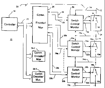
Referring now to FIG. 1, the control arrangement and method of the present
invention will be described in connection with an illustrative system 15 that
includes a
controller 18 that monitors the condition and operating parameters of various
components of the system 15 and takes appropriate action to optimize operation
thereof, e.g. the operating characteristics of an illustrative electronic
switch stage 10 are
monitored as will be explained in more detail hereafter. As illustrated, the
electronic
switch stage 10 includes a main path between lines 12 and 14 that is
controlled
between on and off states, corresponding to respective conductive and non-
conductive
states, via a control connection at 16. In a specific illustrative example,
the electronic
switch stage 10 is a thyristor, IGBT, TRIAC, pair of inverse-parallel
connected SCR's, or
other actively controlled device.
-2-
CA 02385434 2002-05-08
The system 15 includes an illustrative communications arrangement 22 that
cooperates with the controller 18 to provide information to the controller 18
over
communications lines at 20, which in specific embodiments is formed by one or
more
data buses and/or control lines. In the illustrative embodiment, the
communications
arrangement 22 includes a switch control/monitor stage 30 that is located in
the vicinity
of the system component to be monitored, e.g. the electronic switch stage 10,
and that
transmits monitored information to a communications encoder/multiplexer stage
26,
"comm. encoder/mux" 26 hereafter, via a communications link 28, e.g. a
dielectric
medium such as fiber optics in a specific embodiment. As illustrated, where
multiple
components are monitored by the system 15, multiple switch control/monitor
stages 30
are provided along with multiple communication links 28, e.g. 28a, 28b. The
comm.
encoder/mux stage 26 then functions to multiplex the information on the
various
communication links 28 and provides the information in a predetermined
multiplexed
format at 20 to the controller 18.
The control connection 16 of the electronic switch stage 10 is connected to a
gate drive signal at 24 provided by the switch control/monitor stage 30. In
this
illustrative example, the system 15 monitors the gate drive signal at 24
and/or the
temperature of the switch stage 10 via data at 32. This arrangement is
especially
useful where the illustrative electronic switch stage 10 or various other
component is
located remotely from the controller 18 and/or where the illustrative
electronic switch
stage 10 is located in a more severe environment that is deleterious for the
controller
18, e.g. high-noise, medium voltage, high-temperature etc. In one specific
embodiment, the temperature of the switch stage 10 is measured at the location
of the
switch control/monitor stage 30 with the switch control/monitor stage 30 being
in the
proximate vicinity of the switch stage 10, e.g. on a common mounting
arrangement or
heat sink 34 (not shown in detail).
Considering now an illustrative embodiment of the communications arrangement
22 of the system 15 and referring now additionally to FIG. 2, the information
on the
communication link 28 includes a representation of the gate drive signal 24,
such that a
pulse signal 40 is sent over the communications link 28 when the electronic
switch
stage 10 is conducting. The pulse signal 40 is sent on a repetitive basis,
e.g. each
basic clock cycle or each half-cycle of a fundamental waveform that is present
on the
line 12 to the electronic switch stage 10. The receipt of this signal 40 by
the comm.
encoder/mux stage 26 and the transmission of this representation to the
controller 18
-3-
CA 02385434 2002-05-08
over lines 20 also indicates that the communications arrangement 22 is
operational and
that the electronic switch stage 10 is not shorted.
In the illustrative embodiment of FIG. 1, the electronic switch stage 10 is
one
stage of an overall series-connected electronic switch, e.g. six stages as
depicted in
FIG. 1 by a second stage 10a and a sixth stage 10b. Also provided for each
stage is
one of the switch control/monitor stages 30, e.g. 30, 30a, 30b which transmits
a signal
on each of the communication links 28, e.g. 28, 28a and 28b, to the comm.
encoder/mux stage 26. For example, as depicted in FIG. 2, respective signals
42 and
44 are transmitted for the second and sixth electronic switch stages 1 Oa and
1 Ob which
are generated simultaneously and repetitively. The comm. encoder/mux stage 26
then
multiplexes the received pulse signals, e.g. 40, 42 and 44, and provides the
multiplexed
signal at lines 20 to the controller 18. Accordingly, the receipt by the
controller 18 of the
continuous train of pulses verifies that each switch stage of the stages 10,
10a, 10b
etc., denoted as 1 Ox hereafter, is conducting. If the pulses are not
continuous, e.g. not
present in the predetermined pattern and spacing as shown in FIG. 3, i.e. one
or more
of the pulses are missing at the periodic rate, then the controller 18 is
advised/alerted
that something is wrong with either one of the electronic switch stages 1 Ox
or the
communication arrangement 22. If the pulse train of multiplexed signals at 20
is
synchronized to the controller 18, the controller 18 can identify which of the
stages has
a malfunction, e.g. stage 3 in FIG. 3 as indicated by the missing pulse
denoted 62.
Considering now an illustrative embodiment where additional information is
transmitted over the communications arrangement 22 and referring now
additionally to
FIG. 4, it is desirable for the controller 18 to ascertain additional
information about the
various components of the system 15, e.g. the temperature of the electronic
switch via
the sensed temperature signal 32. To accomplish the communication of
additional
information, the switch control/monitor stage 30 encodes additional
information along
with the gate driver signal information, e.g. as shown in FIG. 4 by the
addition of a pulse
signal 50 that represents temperature of the electronic switch stage 10 along
with a
representation of the gate driver signal, e.g. pulse signal 52. In a specific
arrangement,
the width of the pulse 50 is proportional to the sensed temperature at 32.
Thus, the
pulse signals 50, 52 are sent over the communications link 28 on a periodic
basis, e.g.
as discussed before, for each basic operational cycle of the system 15. For
example,
pulse signals 50, 52 correspond to a switch control/monitor stage 30
associated with a
first electronic switch stage 10 and pulse signals 54, 56 correspond to the
stage 30a
-4-
CA 02385434 2002-05-08
associated with a second electronic switch stage 10a. It should be noted that
in FIG. 4,
while the pulses are shown sequentially for each stage, the pulses for each of
the
stages is sent repetitively and simultaneously, the representation in FIG. 4
being the
multiplexed sequential arrangement performed by the comm. encoder/mux stage 26
in
response to the continuous information received from the various stages on the
communication links 28, 28a, 28b etc.
In a specific embodiment, the comm. encoder/mux stage 26 also incorporates an
,ambient temperature signal to the controller 18. For example, with additional
reference
to FIG. 5, after the comm. encoder/mux stage 26 outputs a sequence of pulses
corresponding to each of the stages, an ambient temperature signal 60 is
encoded or
multiplexed into the pulse train in place of the first stage signal or other
position. Thus,
the controller 18 receives a pulse train of signals representing the gate
signal and the
temperature of each of the switch stages 10x followed by the ambient
temperature of
the environment of the controller 18 and the comm. encoder/mux stage 26. In
this
manner, the temperature rise of each switch stage 10 above the ambient
temperature is
available. Additionally, as shown in FIG. 5, the absence of a pulse signal for
any of the
stages, e.g. at 63 for stage 3, indicates a malfunction of the communications
link or the
gate drive signals or the shorted condition of the respective switch stage 10
etc.
In accordance with additional aspects of the present invention, and referring
now
additionally to FIG. 6, in a preferred embodiment, the gate driver signal
pulse 40 is
transmitted over the communications link 28, on a normal basis in one specific
embodiment , or in another specific embodiment, upon a requested basis as
determined by the controller 18. For example, the controller 18 issues a
request signal,
as illustrated at 64 in FIG. 6, on a communications line 29, e.g. a dielectric
medium
such as fiber optics in a specific embodiment, to instruct/condition the
switch
control/monitor stage 30 to initiate the transmission of the combined
additional
information of the gate signal and the temperature of the switch stage 10.
Thus, the
stage 30 sends the normal signals as shown in FIG. 2 until a request signal is
received
whereupon the signals depicted in FIG. 4 are sent, all as depicted in the
sequence of
FIG. 6.
In accordance with yet additional aspects of the present invention, the
controller
118 over the communication lines at 20 is arranged to issue predetermined ON
or OFF
signals to control the conductive state of the switch stages 10 to 10b over
the
communications link 29 of the communications arrangement 22. In response to
the ON
-5-
CA 02385434 2002-05-08
or OFF signals at 20, the switch control/monitor stage 30 sends a gate drive
control
signal at 24 to turn the switch on or off in accordance with the received
signal. For
example, signals at 20, either on one line or as a coded representation, are
responded
to by the comm. encoder/mux stage 26 which issues an ON signal representation
over
the communications link 29 to the switch control/monitor stage 30. The switch
control/monitor stage 30 decodes the ON signal representation on the
communications
link 29 and outputs a signal at 24 to the switch stage 10. In one embodiment,
a
momentary ON signal at 20 causes the stage 30 to turn the switch stage 10 on
and the
switch stage 10 is turned off only upon the issuance of a momentary OFF signal
at 20.
In another embodiment, the ON signal is continuously output at 29 until the
switch
control/monitor stage 30 responds with one or more predetermined signals over
the
communication link 28 to acknowledge that the ON signal has been received and
acted
upon and/or that the switch stage 10 is conducting, e.g. as shown at 65 or 66
in FIG. 5.
In a specific embodiment, the ON/OFF signals at 20 are encoded over the
communications link 29 as a pulse train of a predetermined number of pulses,
the ON
and OFF signals being a different number of pulses. The comm. encoder/mux
stage 26
encodes the pulse train and the switch control/monitor stage 30 counts the
pulses of
the signal and determines whether or not the received signal is an ON or OFF
signal.
In one embodiment, the request for diagnostic signal issued by the comm.
encoder/mux
stage 26 at 29 is a third signal, e.g. a different number of pulses than the
ON or OFF
signal representations In another embodiment, the request for diagnostic
signal to start
the transmission of temperature signals over the communication link 28 is the
transmission of a predetermined "ON" signal over the link 29. Considering
another
illustrative embodiment of the present invention and referring now
additionally to FIG. 7,
the temperature signal alone is communicated via the communications
arrangement 22
of FIG. 1, e.g. signal 50 for stage 10, 54 for stage 1Oa, and the signal 60
for ambient
temperature at the stage 26. In another embodiment, a distinct ready signal is
utilized
by the comm. encoder/mux stage 26 to ready the switch stages 1 Ox for
operation in
response to an ON command being received from the controller 18 when the
switch
stages 10x are non-conducting. In such cases, the switch control/monitor
stages 30
respond to the detection of the distinct ready signal, e.g. predetermined
number of
pulses at 29, by sending a signal such as 40 in FIG. 1 or 65 or 66 of FIG. 5
over the
communications link 28. When the signals are received by the comm. encoder/mux
-6-
CA 02385434 2002-05-08
stage 26, it can be determined that the switch stages 1 Ox are ready for
operation and
ON signals can be issued over the communication links 29.
The system 15 in a preferred embodiment is applied to a multi-phase electrical
power distribution system operating at medium voltages. Accordingly, as shown
in FIG.
1, the system 15 includes additional comm. encoder/mux stages 26, e.g. 26-2
and 26-3
for respective second and third phases of an electrical power source. In one
embodiment, the stages 26, 26-2 and 26-3 are connected to receive signals from
the
controller 18 over a common data bus 20 while in other embodiments the
signaling
paths are independent. In such systems, when the power electronic switch of
stages
10, 1Oa, 1 Ob etc. is non-conducting, it may be desirable to verify its
readiness for
operation, especially when it may be called upon for rapid, high-speed
operation in a
high-speed source-transfer application. In one embodiment, and referring now
to FIG.
8, when the comm. encoder/mux stage 26 receives a signal at 20 from the
controller 18
representing that the switch stages 1 Ox are to be tested, the comm.
encoder/mux stage
.26 issues ON commands to a first portion of the switch control/monitor stages
30, e.g.
N/2 where there are N total switch stages 10x, or (N+1)/2 where N is an odd
number,
and thereafter issue ON commands to the remaining switch control/monitor
stages 30.
Accordingly, the information representing operation of the various switch
stages 10x is
provided to the controller 18 as shown in FIG. 8, first for the first three
stages then for
the next three stages. This is useful because a non-conducting switch can be
tested
while the overall switch remains non-conducting. Additionally, in a preferred
embodiment, the ambient temperature is also provided, as shown at 60 in FIG.
8. As
before, in various embodiments, this can be done with the temperature
representations
for each stage as shown in FIG. 8 or without the individual temperature
representation
signals.
Referring now to FIG. 9, a power electronic switching system functioning as a
high-speed source transfer switching system (HSSTSS) 110 is illustrative of a
specific
system application for which the control arrangement and method of the present
invention of FIGS. 1-8 is useful. The HSSTSS 110 supplies a load at 114 with
an
alternating-current waveform via either a first AC source at 116 or a second
AC source
at 118. The first and second AC sources 116 and 118 and the load at 114 as
provided
in an electrical power distribution system are typically multi-phase circuits
which are
represented in FIG. 9 by a one-line diagram. The HSSTSS 110 includes a first
solid-
state switch, SSS1, 120 and a second solid-state switch, SSS2, 122, which can
also be
-7-
CA 02385434 2002-05-08
characterized as electronic switches or power electronic switches. The HSSTSS
110
via a system control 112 controls either SSS1 to supply the load at 114 via
the first
source 116 or controls SSS2 to supply the load at 114 via the second source
118. In a
specific embodiment, the system control 112 includes the controller 18 of FIG.
1. The
system control 112 provides appropriate control signals at 128, 130 to control
the
operation of each respective solid-state switch, SSS1 120 and SSS2 122. In the
specific illustrative embodiment, the system of FIG. 9 utilizes the
communications
arrangement 22 of FIG. 1. Accordingly, the control signals at 128, 130 are
utilized by
the communications arrangements 22-1 and 22-2 to control the respective solid-
state
switches SSS1 120 and SSS2 122 over respective gate drive signal arrangements
24-1
and 24-2.
In operation, the system control 112 samples the voltage waveforms of each
source 116, 118, e.g. via respective sensing inputs at 124, 126 to detect when
transfer
between the sources is desirable, e.g. sensing outages and momentary
interruptions as
well as voltage sags and swells based on the source supplying the load being
above or
below preset levels. For example, assume that SSS1 120 is turned on by the
system
control 112 via signals at 128 so as to be conductive and supply the load at
114. If the
system control 112 via the sensing input 124 senses that the voltage of the
first source
at 116 is exhibiting undesirable characteristics, the system control 112 via
the control
signals at 128, 130 turns off SSS1 and turns on SSS2 so as to transfer the
supply of
the load at 114 from the first source at 116 to the second source at 118. As
used
herein, the term "incoming" is used to describe the source and the SSS that
will be
turned on to supply the load (e.g. the second source at 118 and SSS2 in the
illustrative
example), and the term "outgoing" is used to describe the source and the SSS
that is
being turned off (e.g. the first source at 116 and SSS1 in the illustrative
example).
Referring now to FIG. 10, each of the solid-state switches SSS1 and SSS2
includes one or more arrays of inverse parallel connected thyristors, e.g.
140a and
140b for SSS1 and 142a and 142b for SSS2. In illustrative implementations,
each array
of thyristors is rated in the range of 2-12 kv. To provide operation in medium
voltage
systems, e.g. operating in the range of 2-34.5 kv, one or more of such
thyristors SSS1
and SSS2 are connected in series for each phase of the sources, e.g. a
plurality of
such thyristors being referred to as a stack. Thus, while the term thyristor
is used for
the solid-state switches SSS1, 140 and SSS2, 142, in specific implementations
at
medium voltages, this commonly refers to a thyristor stack. For example, in a
specific
-8-
CA 02385434 2002-05-08
embodiment, each of the solid-state switches SSS1 and SSS2 is implemented by a
plurality of the switch stages 10x of FIG. 1.
Considering now operation of the control arrangement and method of the
present invention, transfer of the load at 114 from one source to the other,
e.g. the first
source at 116 to the second source at 118, is generally accomplished by
removing the
gating signals at 128a, 128b to shut off SSS1 and starting the gating signals
at 130a,
-130b to turn on SSS2. Thus, the first source at 116 ceases to supply the load
at 114
and the second source at 118 begins to supply the load at 114. For desirable
transfer
control, the controller 112 is provided with additional sensing inputs, e.g.
the incoming
source-voltage differential is determined by the load voltage at 114 as sensed
via a
sensing input 127 or by the differential of the source voltages sensed at 124,
126, and
the current to SSS1 and SSS2 being sensed via respective current sensing
inputs at
'129 and 131.
In accordance with additional aspects of the present invention, the system
control 112 is provided with features to respond to an overheated condition of
the solid
state switches SSS1 and SSS2 to transfer the load at 114 to the alternate
source. For
example, if the temperature sensed via either the communications arrangement
22, or a
separate temperature sense line 150 in a specific embodiment, indicates an
overheated
condition, the system control 112 proceeds with a high-speed transfer. The
system
control 112 then denotes the alternate source as the preferred source. The now
denoted alternate source with the overheated switch is still available on a
temporary
basis for transfers when the system control 112 detects voltage disturbances
on the
source currently feeding the load such that transfer is required. In an
illustrative
embodiment, the overheated condition is defined by any stage of a solid-state
switch
SSS having a sensed temperature that exceeds the ambient temperature by a
predetermined differential. i.e. temperature rise. For example, with reference
to FIG. 1,
if any electronic switch stage 10 has a sensed temperature at 32 that exceeds
the
predetermined limits, an overheated condition is determined.
When an overheated condition is detected, if it is not possible to transfer to
another viable source, the system 110 includes additional features to initiate
and
accomplish a backup transfer to bypass and isolate the switches SSS1 and SSS2
of
the system 110. Specifically, in an illustrative embodiment, as shown in FIG.
9, to
accomplish a bypass/isolation sequence, the system controller 112 controls two
bypass
switches BP-1 and BP-2 and two isolation switches I-1 and 1-2. The switches BP-
1, BP-
-9-
CA 02385434 2002-05-08
2, I-1 and 1-2 are controlled via respective control lines 160, 162, 164 and
166. In
accordance with additional features of the present invention, the
bypass/isolation
sequence is performed to assure optimum load continuity, e.g. as described by
the
following steps:
Disable high speed transfer control (maintain SSS1, SSS2 states);
Close bypass switch(es) (e.g. BP-1) to match the presently conducting SSS('s),
e.g. SSS1;
Confirm that the appropriate bypass switches respond;
Open all isolation switches (e.g. I-1, 1-2);
Confirm that the appropriate isolation switches respond;
Remove all gating signals (e.g. at 128, 130) from all SSS's
Enable backup transfer control (e.g. in this case because an SSS is deemed
unusable)
In situations where backup transfer control is enabled, e.g. to perform
maintenance or service, an overheated SSS, or otherwise unusable SSS (e.g. due
to
lack of control), the system control 112 is capable of providing source
transfer control
using the bypass switches BP-1, BP-2, with the isolation switches I-1, 1-2
remaining
open.
In accordance with additional features of the present invention, when
diagnostic
information is received by the system controller 112 indicating a potential
shorted
condition of a switch SSS, e.g. as detected by the loss of the gating signal
40 or 52 for
a particular switch stage 10x in FIGS. 1-8, the system controller 112 will
identify the
switch SSS and the location of the stage within the switch of the potential
problem.
Appropriate flags, alarms etc. are set and issued. However, the system 110
will
continue to operate normally and be fully functional since the switches SSS
are
designed with devices having suitable predetermined ratings sufficient to be
able to
function when one of the switch stages 10x is shorted. If diagnostic
information is
-10-
CA 02385434 2002-05-08
received that identifies a potential shorted condition of a second of the
switch stages
10x within the same phase or pole of a switch SSS, the system controller 112
initiates
the backup transfer mode as discussed hereinbefore and the high-speed transfer
function is disabled. As discussed hereinbefore in connection with diagnostics
of the
operating parameters of the switches such as SSS1 of the system 110 and the
switch
stages 10x of FIG. 1, the loss of the signals 40 or 52 indicates that either
the switch
stage 10x is shorted, the communications arrangement 22 is not functioning or
the gate
drive signals at 24 are not functioning.
Considering yet further additional features of the present invention, the
system
controller 112 also monitors the voltage across each switch SSS that is
supposed to be
in a conducting mode, i.e. the switch SSS that is supplying the load at 114.
For
example, the system controller 112 monitors the differential voltage between
116 and
114 for switch SSS1. If the differential voltage is greater than a
predetermined value,
e.g. 1500v for a 15kV system, the system controller 112 concludes that the
there is a
malfunction. This detected condition could be caused by an isolation switch
being open
(which would not be normal), a blown fuse in the circuit, or the discontinuity
of the
:switch SSS1 (i.e. non-conducting status such as caused by an open circuit or
broken
connection). If this condition is detected and persists for a predetermined
time interval,
e.g. 2 milliseconds, the system controller 112 initiates a transfer to the
second source
118 by turning on the switch SSS2, and also locks out any transfer back to the
switch
SSS1. Of course, if for any reason an alternate viable source is not
available, the
system controller initiates a backup transfer as discussed hereinbefore. In
addition or
as an alternative to the diagnostic testing of non-conducting switches as
discussed
hereinbefore, if a switch SSS1 has not been turned on in a predetermined
period of
time, e.g. one day, the system controller 112 initiates a transfer to
interrogate the switch
SSS1 to verify proper operation to ensure that a viable alternate source is
available if
needed.
In accordance with other aspects of a specific embodiment of the present
invention to detect a shorted switch device in the stack of series-connected
switch
stages, a representation of the voltage across each of the switch stages 10 is
also
monitored and communicated between the switch control/monitor stage 30 and the
comm. encoder/mux stage 26 via the communication link 28. For example, the
voltage
between the lines 12, 14 in FIG. 1 across the switch stage 10 has been found
useful to
determine if the switch stage 10 is shorted. When the switch stage 10 is
conducting,
-11-
CA 02385434 2002-05-08
the voltage differential across 12, 14 is quite low, typically less than
several volts.
When the switch stage 10 is non-conducting and not shorted, as the voltage at
12 rises,
the voltage differential at 12, 14 also rises. However, if the switch stage 10
is shorted,
e.g. a faulty device, the voltage differential at 12, 14 will not rise with
the increasing
'voltage at 12. Instead, it will not increase above several volts.
Accordingly, as soon as
the voltage differential at 12, 14 rises above several volts, it can be
determined that the
:switch stage 10 is not shorted. To avoid any ambiguity, the switch stage 10
can be
considered normal and not shorted as soon as the voltage differential at 12,
14 exceeds
a predetermined threshold voltage, e.g. 20 volts.
Specifically, as shown in FIG. 1, the voltage across the switch stage 10 at
74,
74a, corresponding to the voltage differential between the lines 12, 14, is
provided to
the switch control/monitor stage 30. Similarly, the voltage across the switch
stage 10a
at 74a, 74b is provided to the switch control/monitor stage 30a and so forth
for all the
switch stages 1 On in the overall stack of the particular system 15. Each of
the switch
control/monitor stages 30n compares the voltage across the respective switch
stage
'1 On and compares this voltage to a threshold. A representation of the result
of this
comparison is then sent to the comm. encoder/mux stage 26 over the respective
communication link 28n. For example, in a specific embodiment, a pulse is sent
either
additionally to or in place of the temperature pulse 50 when the voltage
across the
switch stage 10 exceeds the threshold voltage, signifying that the switch
stage 10 is not
shorted. In a specific embodiment, the controller 18 issues a request signal
when it is
desired to check the shorted/normal state of the switch stages 10.
In embodiments where the switch stage 10 is maintained on until it is desired
to
turn the switch stage 10 off, the controller 18 tests the switch stages 10 for
a shorted
condition by first turning the switch stage off before a current zero of the
AC waveform
at 12, the voltage across the switch stage 10 is then monitored, and when the
signal is
received corresponding to a non-shorted switch stage 10, the switch stage 10
is turned
back on as described hereinbefore. If the non-shorted status is not received
after
sufficient time for the AC waveform to rise in voltage, the controller 18 then
concludes
that the switch stage 10 is shorted.
In accordance with a specific embodiment of the present invention, the
communication links 28 and 29 are implemented as a 2-way serial bus with all
communications initiated by the controller 18 via the comm. encoder/mux stage
26.
Thus, the comm. encoder/mux stage 26 polls the switch control/monitor stages
30 to
-12-
CA 02385434 2002-05-08
obtain the desired status information. In one specific arrangement, commands
are sent
by the comm. encoder/mux stage 26 as 8-bit data bytes. Similarly, in response
to the
commands, the switch control/monitor stage 30 transmits corresponding status
linformation as 8-bit data bytes. According to one specific protocol, four
commands are
issued by the comm. encoder/mux stage 26, ON, OFF, Temperature request and
TEST. As discussed hereinbefore, the switch control/monitor stage 30 responds
to the
ON, OFF commands by controlling the gate drive signal 24 to the respective
switch
stage 10. Additionally, in this mode, the switch control/monitor stage 30 also
sends
gate drive signal status information representing the gate drive signal at 24.
When
temperature is desired, the Temperature request command is sent and the switch
control/monitor stage 30 responds with a data byte representing the
temperature
information at 32. When a TEST command is received by the switch
control/monitor
stage 30, the switch stage 10 is turned off and voltage across the switch
stage 10 is
detected. Thereafter, the switch shorted/not shorted data byte is sent, in a
specific
embodiment, in response to a specific command corresponding to the reading of
test
data. In a specific arrangement, the data byte that is sent includes
information to
indicate that the data is in response to a test.
It should be realized that with this arrangement, the commands send and the
status information received can be accomplished with fewer than 8-bit data
bytes and
the status information for both switch shorted/not shorted and gate drive
signal can be
sent to the comm. encoder/mux stage 26 simultaneously. However, during normal
operations, the voltage across the switch stage 10 would indicate a shorted
status
whenever the switch stage 10 is in the ON mode, and would indicated a not
shorted
status whenever the switch stage 10 is in the OFF mode. Further, the use of
the
additional data bits in each byte permits combinations of bit patterns to
avoid incorrectly
interpreted status and ambiguous situations as might occur due to noise
affecting the
data, shifted data bytes being received, etc. For example, eight bits of data
for four
commands permits the selection of very distinct command bytes while also
providing
flexibility for additional commands. Concerning the status information sent
via the
communications link 28 in a specific arrangement, the eight bits in each data
byte
permit the higher order bits to be used to confirm the ON/OFF states 30 and
10,
whether the data being sent is status information, TEST command response mode,
and
the actual data representations such as gate drive signal status and/or switch
shorted/not shorted status. In one specific arrangement, one data bit is used
to
-13-
CA 02385434 2011-09-16
represent switch shorted/not shorted status, another bit is used to represent
gate drive
signal status, and a third bit is used to represent normal status or response
to TEST
command. In this arrangement, when temperature data is requested, a
representation
of the temperature is sent using those three data bits.
While there have been illustrated and described various embodiments of the
present invention, it will be apparent that various changes and modifications
will occur
to those skilled in the art. Accordingly, it is intended in the appended
claims to cover all
such changes and modifications that fall within the scope of the present
invention.
-14-