Note: Descriptions are shown in the official language in which they were submitted.
CA 02385562 2002-03-22
WO 01/22446 PCT/USOO/25045
SPLIT INDUCTOR WITH FRACTIONAL TURN OF EACH WINDING
AND PCB INCLUDING SAME
TECHNICAL FIELD
The invention relates generally to logic integrated circuits and more
particularly, to a simplified split winding inductor configuration, easily
adapted
to a synchronous rectifier circuit. More particularly, the present invention
provides an output inductor for a power module that integrates the output
inductor winding into the printed circuit board assembly to decrease the cost
and complexity of the design and improve noise performance.
BACKGROUND OF THE INVENTION
The growth of the distributed power market has lead to increased
research in the area of power modules. As a result, the power density of
power modules has increased four times in the past few years and the
efficiency of power modules has significantly increased due to the
5 improvement of current semiconductor devices and the utilization of
synchronous rectification for power module applications. As logic integrated
circuits have migrated to lower working voltages in the surge for higher
operating frequencies and as overall system sizes have continued to
decrease, power supply designs with smaller and higher efficiency power
10 modules are in demand.
In an effort to improve the efficiencies and increase power densities,
synchronous rectification has become necessary for these types of
applications. Synchronous rectification has gained great popularity in the
last
ten years as low voltage semiconductor devices have advanced to make this
a viable technology. The power electronics design engineer, however, is still
challenged to design power modules with high power density, high efficiency,
low output voltage and high output current.
-1-
WO 01/22446 CA 02385562 2002-03-22 pCT/US00/25045
Power modules having synchronous rectification have generally
comprised a single winding output inductor connected to the output load of
the synchronous rectifier circuit. This has generally been the most popular
approach because of its simplicity and reduced part count. A power module
configuration known as a "quarter brick" can be used in applications where
board space is limited. One version of a quarter brick power module
measures 2.28" long by 1.45" wide by 0.5" in height.
The quarter brick power module, as well as other similar power module
configurations, typically places the input pins and output pins on opposite
ends of the assembly. Essentially, the packaging and layout constraints
require the output inductor to be terminated at opposite ends with respect to
both the input and output sides of the inductor. This configuration results in
a
winding configuration with an extra half turn which, in turn, effects the
resultant magnetic flux patterns of the inductor core. In particular, the
inductance of the fractional turn created by the termination of the output
inductor increases with current so that the inductor is easily saturated.
5 SUMMARY OF THE INVENTION
The present invention achieves technical advantages as a split
inductor that can be easily adapted to a synchronous rectifier circuit as an
output inductor. The present invention, which comprises a new split inductor
design, can be integrated within a quarter brick power module to combine the
10 inductor windings and magnetics onto a scale platform. An optimum layout
and package configuration is attained without compromising the design of the
output inductor.
As such, according to one embodiment, disclosed is a split inductor
15 comprising an inductor core having a first, second, and third legs
extending
from a base member. The first and second legs are predisposed and spaced
about a surface of the base member to form a first channel area. The second
leg also forms, along with the third leg, a second channel area separated
-2-
CA 02385562 2007-09-24
from the first channel area by the second leg. The inductor also comprises
an inductor winding an'anged about the inductor core to provide relatively
equal magnetic flux through the first, second, and third legs when current
flows through the inductor winding.
In one embodiment of the present invention, the split inductor is
integrated within a printed circuit board (PCB) assembly which comprises a
plurality of PCB layers. Each of the PCB layers includes a conductive core
sub-layer predisposed between two base material sub-layers with each
conductive.core sub-layer formed into desired circuit pathways. The PCB
assembly also compnses a plurality of insulation layers predisposed between
the PCB layers and first, second, and third openings extending through the
PCB layers. The openings are arranged to accept an inductor core,
according to the teachings of the present invention, with a corresponding leg
of the inductor core capable of being inserted through a corresponding
opening of the PCB assembly.
In yet another embodiment, the present invention is utilized in a
synchronous rectifier circuit with the split inductor configuration forming
the
output inductor on the secondary side of a synchronous rectifier circuit_
According to an aspect of the present invention there is provided a printed
circuit board (PCB) assembly with an onboard inductor comprising:
a plurality of PCB layers, each of said layers including a conductive core sub-
layer predisposed between two base material sub-layers, each conductive core
sub-layer formed into circuit pathways, said circuit pathways adapted to
connect
circuit components to said PCB assembly;
a plurality of insulation layers predisposed between each PCB layer;
an inductor core having a base with first, second and third legs extending
therefrom;
first, second and third openings extending through said plurality of PCB
layers,
said openings adapted to accept said inductor core; and
3
CA 02385562 2007-09-24
split inductor windings integrated into said plurality of PCB layers and
arranged
about said inductor core in order to balance the magnetic flux in each of said
first, second and third legs;
wherein said split inductor windings adapted to provide an equal number of
signal paths through a first area defined by said first and second openings
and
through a second area defined by said second and third openings.
A technical advantage of the present invention is the easy adaptation
of the inductor configuration of the present invention into power module
assembly such as the quarter brick power module_
Yet another technical advantage of the present invention is that the
new inductor configuration can be used to filter out the common mode noise
and reduce the output noise of the filter circuit.
3a
CA 02385562 2002-03-22
WO 01/22446 PCT/US00/25045
Still another technical advantage of the present invention is the use of
the split inductor configuration of the present invention in other power
supply
circuit topologies such as full bridge and push-pull.
BRIEF DESCRIPTION OF THE DRAWINGS
The above features and advantages of the present invention will be
more clearly understood from consideration of the following descriptions in
connection with accompanying drawings in which:
Figure 1 is an illustration of the prior art single inductor configuration in
a synchronous rectifier circuit;
Figures 2A-C illustrate equivalent configurations for an output inductor
having a load Co;
Figure 3 shows the split inductor of the present invention;
Figure 4A is a top view of the present invention with an unequal
number of winding turns;
Figure 4B illustrates the magnetic properties of the present invention
with an unequal number of winding turns;
Figure 5A is a top view of the present invention with an equal number
of winding turns;
Figure 5B illustrates the magnetic properties of the present invention
with an equal number of winding turns;
Figure 6 are simple diagrams of the voltage inputs and outputs for a
printed circuit board;
-4-
WO 01/22446 CA 02385562 2002-03-22 pCT/US00/25045
Figure 7 is a simple block diagram of a printed circuit board with
synchronous rectification;
Figure 8A illustrates the layers of the printed circuit board in which the
present invention is integrated;
Figure 8B is a top view of the printed circuit board;
Figure 9 is a circuit schematic of the present invention as
implemented as a synchronous rectifier circuit; and
Figure 10A and 10B illustrates the differential noise of the prior art
circuit and the circuit of the present invention.
Corresponding numerals and symbols in the different figures refer to
corresponding parts unless otherwise indicated.
DETAILED DESCRIPTION OF PREFERRED EMBODIMENT
The following is a description of the present invention. A prior art half-
bridge DC-to-DC converter circuit will be discussed first, followed by a
description of several preferred embodiments of the present invention, and a
discussion of the advantages.
Figure 1 is an illustration of the use of a single inductor Lo in a
synchronous rectifier circuit 10 for a half bridge DC- to-DC converter. The
synchronous rectifier circuit 10 comprises a primary transformer T1 having a
primary and a secondary winding 11 and 12, respectively. The synchronous
rectifier circuit 10 also comprises an external drive circuit 18, which is
used to
drive the synchronous rectifiers Q1 and Q2.
-5-
WO 01/22446 CA 02385562 2002-03-22 pCT/US00/25045
In particular, the first and second synchronous rectifiers Q1 and Q2 are
operably coupled to the primary transformer T1 and the external drive circuit
18. The timing signals which turn on and off the synchronous rectifiers Q1
and Q2 are derived from the external drive circuit 18. This timing information
is then transferred from the primary side to the secondary side 16 of the
rectifier circuit 10 utilizing primary transformer T1.
Traditionally, a single output inductor Lo is used as shown in Figure 1.
According to the prior art, the use of a single inductor Lo is preferred
because
of its simplicity and reduced part count. However, in some applications the
output inductor Lo is split into two identical windings connected at each side
of the output capacitor to increase common mode noise rejection. Obviously,
a two winding structure results in increased cost and complexity. Another
approach is to wind two windings over the same inductor core, but this
configuration increases the complexity of the manufacturing process. What is
needed is a inductor configuration which increases common mode noise
rejection but does not increase the complexity of the manufacturing process.
The present invention provides such a configuration for the output inductor in
a power module assembly useful in synchronous rectifiers such as that shown
in Figure 1.
Figures 2A-C illustrate equivalent configurations for an output inductor
of a synchronous rectifier circuit. Figure 2A shows the traditional single
inductor configuration as discussed above. The single inductor Lo may be
split into two identical windings L1 and L2, as shown in Figure 2B, and placed
in series with an output capacitor Co. This configuration, however, does not
provide the needed filtering of noise in the circuit. To increase common mode
noise rejection, the two identical windings L1 and L2, shown in Figure 2B,
may be re-configured by placing the windings L1 and L2 at each side of the
output capacitor as shown in Figure 2C.
-6-
WO 01/22446 CA 02385562 2002-03-22 pCT/US00/25045
The present invention is a split inductor configuration having the two
windings connected at each end of the output capacitor. However, the
present invention provides the added advantage of decreased cost and
decreased complexity of the manufacturing process compared to prior art
split inductor configurations of Figures 2A and 2B. To better understand the
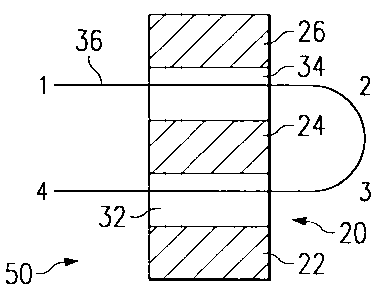
present invention, reference is made to Figure 3, which illustrates an
inductor
core 20 having first, second, and third legs 22, 24, and 26, respectively,
integrally extending from a base member 28. The first leg 22 and second leg
24 are predisposed, spaced and extend substantially perpendicular from a
first surface 30 of the base member 28 to form a first channel area 32.
Likewise, the second leg 24 and the third leg 26 are predisposed, spaced and
extend substantially perpendicular from a second surface 33 to form a second
channel area 34 separated from the first channel area 32 by the second leg
24.
As shown in figure 4A, which is a top view of a three-legged inductor
core 20 suitable for use in the inductor configuration 50 of the present
invention, an inductor winding 36 can be wound about the inductor core 20,
creating signal paths in the channel areas 32 and 34. The winding 36 may be
formed of any conducting material such as copper, for example. The winding
36 as arranged, however, results in one whole turn about the first leg 22,
second let 24, and third leg 26, respectively, and an additional fractional
turn
38 between the second leg 24 and third leg 26. This fractional turn 38 results
in one signal path through the first channel area 32 and two signal paths
through the second channel area 34. The effective inductance created by the
fractional turn 38 will vary with current and can easily saturate the output
inductor Lo, which is undesirable.
The saturation phenomenon is illustrated in Figure 4B which shows the
magnetic circuit of an inductor Lo with a fractional turn 38. P1, P2, P3 is
the
permeance of the first, second, and third legs 22, 24, and 26, respectively.
-7-
WO 01/22446 CA 02385562 2002-03-22 PCT/USOO/25045
FIux1, Flux2, and Flux3 represent the magnetic flux that goes through each
leg 22, 24, and 26. N*I and 1*1 are the MMFs in each leg. As the current
increases, more flux is pushed away from the third leg 26 into the second leg
24. Essentially, the effective inductance reduces as the load current
increases. Eventually the inductor core 20 will be saturated because too
much of the flux is pushed into the second leg 24.
The present invention provides an inductor configuration 50 wherein
the inductor winding 36 is arranged about the inductor core 20 to balance the
magnetic flux in each leg 22, 24, and 26. In order to provide relatively equal
magnetic flux through the first, second, and third legs 22, 24, and 26,
respectively, when current flows through the inductor winding 36, the inductor
winding 36 is arranged to provide an equal number of signal paths through
the first channel area 32 defined by the first leg 22 and second leg 24 and
the
second channel area 34 defined by the second leg 24 and third leg 26. This
configuration, denoted generally as 50, is shown in Figures 5A.
Figure 5B shows the equivalent magnetic circuit for the inductor
configuration, according to the invention. The MMFs and permeance in the
first leg 24 and third leg 26 is exactly the same so that the magnetic flux is
balanced in the first let 24 and third leg 26. The fact that equal number of
signal path are created in the channel areas 32 and 34 means that the
inductor core 20 will not saturate.
Accordingly, the inductor configuration 50 may be integrated within a
printed circuit board (PCB) assembly and used as an output inductor Lo for a
synchronous rectifier circuit suitable for use in power regulation
applications.
The inductor configuration 50 is shown with the output inductor of a quarter
brick power module as an example, but the present invention provides a
general solution in optimizing the PCB package and layout without
compromising the design of input and/or output inductors.
-8-
WO 01/22446 CA 02385562 2002-03-22 PCT/USOO/25045
Figure 6 shows a typical mechanical representation of a standard
quarter brick power module 40. The packaging and layout constraints require
the output inductor to be terminated at opposite sides of the structure
resulting in a winding with a half turn. As shown, the input pins Vin+ and Vin-
and output pins Vout+ and Vout- are located at opposite ends of the module.
The normal part location for a power brick module 40 is shown in the figure 7.
The module 40 can be divided into the sections of a primary switch 42,
transformer 44, rectifiers 46, output inductor 48 and output capacitors 49.
The ideal situation is that the current goes into the inductor section 48 from
rectifier section 46 of the inductor (terminal 1 close to the rectifier
section),
and comes out at the output capacitor 49 (terminal 2 close to the output
capacitor section).
Figure 8A illustrates the layers of the printed circuit board (PCB) 51 in
which inductor configuration 50 of the present invention can be integrated.
The PCB 51 comprises a plurality of PCB layers 53. Each of the PCB layers
53 includes a conductive core sub-layer 52 predisposed between two base
material sub-layers 54. The conductive core sub-layer 52 may comprise any
conducting material such as aluminum or copper, for example, or other
similar conductor. Each conductive core sub-layer 52 is formed into the
desired circuit pathways which are utilized to connect the circuit components
(i.e. inductor, capacitors, transformer, etc.) to the assembly 51.
The PCB 51 also comprises a plurality of insulation layers 56
predisposed between the PCB layers 53 within first, second, and third
openings 58, 60, and 62, respectively (shown in Figure 8B), extending
through the plurality of PCB layers 53 and arranged to support the insertion
of
the three-legged inductor core 20. In particular, each leg 22, 24 and 26 of
the
inductor core 20 would be inserted into a corresponding opening 58, 60 and
62. A portion of each conductive core sub-layer 52 is further formed into a
-9-
WO 01/22446 CA 02385562 2002-03-22 PCT/US00/25045
split inductor winding 36 which provides an equal number of signal paths
through the first and second channel areas 32 and 34.
The process and fabrication techniques of forming such an inductor
winding 36 within the core sub-layers 52 is well known in the art. The
inductor winding 36 can be split into two winding portions (not shown)
containing a half-turn to optimize the package and layout requirements, but
with an effective winding containing no half or fractional turns. Therefore,
the
PCB 51 is optimized without compromising the design and performance of
the inductor.
An advantage of the PCB 51 is that the power module can be
integrated with the magnetics to further simplify the manufacturing process
since the inductor windings 36 are buried inside the PCB 51 and no
termination is required.
A circuit schematic illustrating the split inductor configuration 50 in a
synchronous rectifier circuit is shown and denoted generally as 100 in Figure
9. The split inductor configuration 50 not only makes the circuit layout much
better, but also filters out the common mode noise and reduces the output
noise. The common mode current is shown in Figures 10A-B. In the
conventional approach, the common mode current that is generated by
switching will produce differential mode noise on the output (Figure 10A)
because of the different impedance in each current path. In the new
approach, the impedance in each current path is similar or can be matched
so that the differential noise will be reduced or no differential noise will
be
generated by the common mode current as shown in Figure 10B.
Furthermore, this concept can be extended to input inductor.
The novel method and system of the present invention provides the
advantage of being cost effective to manufacture using standard fabrication
-10-
WO 01/22446 CA 02385562 2002-03-22 pCT/US00/25045
processes and techniques. Another advantage is the reduction in common
mode noise due to the split inductor winding configuration 50. Yet another
advantage of the present invention is the prevention of saturation of the
inductor core 20.
While the invention has been described with reference to illustrative
embodiments, this description is not intended to be construed in a limiting
sense. Various modifications in combinations of the illustrative embodiments,
as well as other embodiments of the invention, will be apparent to persons
skilled in the art upon reference to the description.
-11-