Note: Descriptions are shown in the official language in which they were submitted.
CA 02387744 2005-05-24
SCANMNG BEAM IMAGE DISPLAY
Tecdnical Field
The present invention relates to low light viewing systems and, more
particularly, to low light viewing systems that produce simulated images for a
user.
Background of the Invention .
Low sight vision devices are widely used in a variety of applications, such
as night vision goggles ("NVGs"). NVGs allow military, police, or other
persons
to view objects in nighttime or low light environments.
A typical night vision goggle employs an image intensifier tube (IIT) that
produces a visible image in response to light from the environment. ~ To
produce
the visible image, the image intensifier tube converts visible or non-visible
radiation from the environment to visible light at a wavelength readily
perceivable
by a user.
One prior art NVG 30, shown in Figure l, includes an input lens 32 that
couples light from an external environment 34 to an IIT 36. The IIT 36 is a
commercially available device, such as the G2 or G3 series of IITs available
from
Edmonds Scientific. As shown in Figure 2, the IIT 36 includes a photocathode
38
that outputs electrons responsive to light at an input wavelength ~.~. The
electrons
CA 02387744 2002-04-12
WO 01/33866 PCT/US99/25565
enter a microchannel plate 40 that accelerates and/or multiplies the electrons
to
produce higher energy electrons at its output. Upon exiting the microchannel
plate
40, the higher energy electrons strike a screen 42 coated with a
cathodoluminescent layer 44, such as a green phosphor. The cathodoluminescent
layer 44 responds to the electrons by emitting visible light in regions where
the
electrons strike the screen 42. The light from the cathodoluminescent layer 44
thus forms the output of the IIT 36.
Returning to Figure I, the visible light from the cathodoluminescent layer
44 travels to eye coupling optics 46 that include an input lens 48, a beam
splitter
50, and respective eyepieces 52. The lens 48 couples the visible light to the
beam
splitter 50 that, in turn, directs portions of the visible light to each of
the eyepieces
52. Each of the eyepieces 52 turns and shapes the light for viewing by a
respective one of the user's eyes 54.
As is known, common photocathodes are often quite sensitive in the IR or
near-IR ranges. This high sensitivity allows the photocathode to produce
electrons
at very low light levels, thereby enabling the IIT 36 to produce output light
in very
low light conditions. For example, some NVGs can produce visible images of an
environment with light sources as dim or dimmer than starlight.
Often, users must train to properly. and effectively operate in low vision
environments using NVGs for vision. For example, the lenses 48, IIT 36 and
eyepieces 52 may induce significant distortion in the viewed image.
Additionally,
the screen 42 typically outputs monochrome light with limited resolution and
limited contrast. Moreover, NVGs often have a limited depth of field and a
narrow field of view, giving the user a perception of "tunnel vision." The
overall
optical effects of distortion, monochromaticity, limited contrast, limited
depth of
field and limited field of view often require users to practice operating with
NVGs
before attempting critical activities.
In addition to optical effects, users often take time to acclimate to the
physical presence of NVGs. For example, the NVG forms a mass that is displaced
2
CA 02387744 2002-04-12
WO 01/33866 PCT/US99/25565
from the center of mass of the user's head. The added mass induces forces on
the
user that may affect the user's physical movements and balance. Because the
combined optical and physical effects can degrade a user's performance
significantly, some form of NVG training is often required before the user
engages
in difficult or dangerous activities.
One approach to training, described in U.S. Patent No. 5,420,414, replaces
an IIT with a fiber rod that transmits light from an external environment to
,the
user. The fiber rod is intended to limit the user's depth perception while
allowing
the user to view an external environment through separate eyepieces of a
modified
NVG. The fiber rod system requires the IIT to be removed and does not provide
light at the output wavelength of the cathodoluminescent layer. Additionally,
the
fiber rod system does not appear to provide a way to provide electronically
generated images.
An alternative approach to the fiber rod system is to project an
electronically generated IR or near-IR image onto a large screen that
substantially
encircles the user. The user then views the screen through the NVG. This
system
has several drawbacks, including limiting the user's movement and orientation
to
locations where the screen is visible through the NVG.
Moreover, typical large screen systems utilize projected light to produce the
screen image. One of the simplest and most effective approaches to projecting
light onto a large surrounding screen is to locate the projecting source near
the
center of curvature of the screen. Unfortunately, for such location, the user
may
interrupt the projected light as the user moves about the artificial
environment. To
avoid such interruption, the environment may use more than one source or
position the light source in a location that is undesirable from an image
generation
point-of view.
3
CA 02387744 2005-05-24
Summary of the Invention
The present invention provides a display device that produces a visible image
in
response to an input image signal having a plurality of components,
comprising: a
screen, including a base plate and a wavelength converting coating responsive
to output
light of a first visible wavelength range in response to light of a first
input wavelength,
and responsive to output light of a second visible wavelength range in
response to light
of a second input wavelength; a first light emitter operative to emit
modulated light of
the first input wavelength in response to a first component of the image
signal; a second
light emitter operative to emit modulated light of the second input wavelength
in
response to a first component of the image signal; and a scanner assembly
having an
input aligned optically to receive light from the first and second light
emitters and an
output aligned optically to direct the light received at the input to the
screen, the scanner
assembly being responsive to a driving signal to scan the received light onto
the
wavelength converting coating in a periodic pattern including at least one
dimension, the
scanner assembly being further responsive to the drive signal to scan the
received light
bidirectionally in the at least one dimension.
The present invention also provides a head mounted display, comprising: an
image signal source that produces an image signal corresponding to a desired
image; a
screen having a wavelength converting coating, the coating being responsive to
non-
visible radiation to emit visible light; a light source responsive to the
image signal to
emit non-visible radiation modulated according to the image signal; and a
scanner
positioned to receive the modulated light and operative to scan the received
light onto the
screen in a periodic pattern having at least one dimension and to scan the
received light
resonantly in the at least one dimension.
According to one embodiment of the invention, a display apparatus includes a
night vision goggle (NVG) and an infrared source. In one embodiment, the
infrared
source is a scanned light beam display that includes a scanning system and an
infrared
light emitter. The infrared source receives an image signal from control
electronics that
indicates an image to be viewed. The control electronics activate the light
emitter and the
light emitter emits modulated light having an intensity corresponding to the
desired
4
CA 02387744 2005-05-24
image. Simultaneously, a scanning mirror within the scanning system scans the
modulated light through a substantially raster pattern onto an image
intensifier tube of
the night vision goggles.
In response to the incident infrared light (IIT), the IIT outputs visible
light for
viewing by a user. To prevent environmental light from affecting the IIT, the
input to the
IIT is occluded, in one embodiment.
In one embodiment that includes a scanner, the scanner includes two uniaxial
scanners, while in another embodiment, the scanner is a biaxial scanner. In
one
embodiment, the scanner is a mechanically resonant scanner. The scanner may be
a
discrete scanner, acousto-optic scanner, microelectromechanical (MEMs) scanner
or
another type of scanner.
In an alternative embodiment, the scanner is replaced by a liquid crystal
display
with an infrared back light. The LCD is addressed in conventional fashion
according to
image data. When a pixel is activated, the pixel transmits the infrared light
to the IIT. In
response, the IIT outputs visible light to the user.
In another alternative embodiment, the scanner is replaced by an emitter panel
of
a field emission display. In this embodiment, the IIT photocathode may also be
removed.
The emitter panel then emits electrons directly to the microchannel
accelerator of the
NVG. The accelerated electrons activate the cathodoluminescent material of the
NVG to
produce output light for viewing.
In still another embodiment, a non-visible radiation source, such as an
ultraviolet
or infrared light source illuminates a phosphor. In response, the phosphor
emits light at
visible wavelengths. In one embodiment, where the non-visible radiation source
is
infrared, the wavelength is selected in a region that is determined to be safe
for human
viewing.
In another embodiment of the invention, a display uses a plurality of non-
visible
radiation sources, such as laser diodes, to drive wavelength selective
phosphor
compounds on a screen. Each of the phosphor compounds is responsive to a
selected one
of the light sources to emit visible light at a respective visible wavelength.
An electronic
controller modulates each of the non-visible radiation sources according to
image
information in an image signal, such as a conventional video signal. A scanner
then
CA 02387744 2005-05-24
scans the modulated light from all of the light sources in a substantially
raster pattern
onto the phosphor compounds. In response the phosphor compounds emit light at
their
respective visible wavelengths with intensities corresponding to the modulated
intensity
of the corresponding non-visible radiation. Each location on the screen thus
emits light
with a color and intensity dictated by the image signal, thereby producing a
respective
pixel of an image.
In a further aspect, the present invention provides a method of providing a
visible
image to a user, comprising the steps of-. producing light of a non-visible
wavelength;
producing light of a first visible wavelength; modulating the light of the non-
visible
wavelength with a first portion of image information; modulating the light of
the first
visible wavelength with a second portion of image information; scanning the
light of the
non-visible wavelength in a first periodic pattern; scanning the light of the
first visible
wavelength in a second periodic pattern; converting the scanned light of the
first non-
visible wavelength into light of a second visible wavelength; and directing
the scanned
first visible wavelength and the converted second visible wavelengths to the
user.
In a still further aspect, the present invention provides a method of
producing an
image for viewing by a user, comprising the steps o~ producing a first
electrical image
signal corresponding to a first portion of the image to be viewed; producing a
second
electrical image signal corresponding to a second portion of the image to be
viewed;
applying the first image signal to a first image source; applying the second
image signal
to a second image source; emitting infrared light of a non-visible wavelength
range in
response to the applied first image signal; emitting visible light of a first
visible
wavelength range different from the non-visible wavelength range in response
to the
applied second image signal; directing the emitted infrared light of the non-
visible
wavelength to a screen that includes wavelength converting material; directing
the
emitted visible light of the first visible wavelength to the screen; emitting
visible light of
a second visible wavelength with the wavelength converting material in
response to the
directed emitted light of the non-visible wavelength; and emitting visible
light of the first
visible wavelength with the screen in response to the directed emitted light
of the first
visible wavelength.
5a
CA 02387744 2005-05-24
Brief Description of the »gures
Figure 1 is a diagrammatic representation of a prior art low light viewer,
including an image intensifier tube (IIT) and associated optics.
Figure 2 is a detail block diagram of the IIT of Figure 1.
Figure 3 is a diagram of a combined image perceived by a user resulting from
the combination of light from an image source and light from a background.
Figure 4 is a diagrammatic representation of a night vision simulator
including
an infrared beam scanned onto a night vision goggle input.
Figure 5 is a side elevational view of a head-mounted night vision simulator
including a tethered IR source
Sb
CA 02387744 2002-04-12
WO 01/33866 PCT/US99/25565
Figure 6 is a schematic of an IR scanning system suitable for use as the
image source in the display of Figure 2.
Figure 7 is a diagrammatic view of an embodiment of a simulator including
a LCD panel with an infrared back light.
Figure 8 is a diagrammatic view of an embodiment of a simulator including
an FED emitter.
Figure 9 is a top plan view of a simulation environment including a
plurality of users and a central control system including a computer
controller and
rf links.
Figure 10 is a diagrammatic view of an embodiment of a display including
a scanned light beam activating a wavelength converting phosphor and a
reflected
visible beam.
Figure 11 is a diagrammatic representation of an embodiment of a head
mounted display including a scanned non-visible radiation beam activating a
wavelength converting phosphor to produce a visible image.
Figure 12 is a diagrammatic view of a color display system using non-
visible radiation sources at a plurality of wavelengths to selectively
activate
wavelength selective phosphors.
Figure 13 is a top plan view of a bi-axial MEMS scanner for use in the
display of Figure 4.
Detailed Description of the Invention
A variety of techniques are available for providing visual displays of
graphical or video images to a user. Recently, very small displays have been
developed for partial or augmented view applications. In such applications,
the
display is positioned to produce an image 60 in a region 62 of a user's field
of
view 64, as shown in Figure 3. The user can thus see both a displayed image 66
and background information 68.
6
CA 02387744 2005-05-24
One example of a small display is a scanned beam display such as that
described in U. S. Patent No: 5,467,104 of Furness et al., entitled VIRTUAL
RETINAL DISPLAY. In scanned
displays, a scanner, such as a scanning mirror or acousto-optic scanner, scans
a
modulated light beam onto a viewer's retina. The scanned light enters the eye
through the viewer's pupil and is imaged onto the retina by the cornea. The
user
perceives an image corresponding to the modulated light image onto the retina.
Other examples of small displays include miniature liquid crystal displays
(LCDs),
field emission displays (FEDs), plasma displays and miniature cathode ray tube-
based displays (CRTs). Each of these other types of displays is well known in
the
art.
As will be described herein, these miniature displays can be adapted to
activate light emitting materials to produce visible images at selected
wavelengths
different from the wavelengths of miniature display. For example, such
miniature
displays can activate the cathodoluminescent material of NVGs to produce a
perceived image that simulates the image perceived when the NVGs are used to
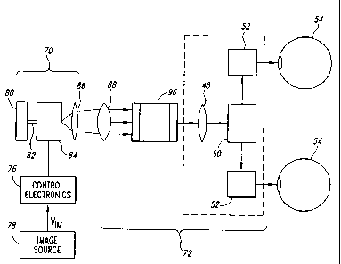
view a low light image environment. A first embodiment of such a system, shown
in Figure 4, includes an IR scanned light beam display 70 positioned to scan a
beam for input to an NVG 72. Responsive to light from the IR display 70, the
hIVG 72 outputs visible light for viewing by the viewer's eyes 54. The IR
display
70 includes four principal portions, each of which will be described in
greater
detail below. First, control electronics 76 provide electrical signals that
control
operation of the display 70 in response to an image signal V,M from an image
source 78, such as a computer, television receiver, videocassette player, or
similar
device. While the block diagram of Figure 4 shows the image source ?8
connected directly to the control electronics 76, one skilled in the art will
recognize other approaches to coupling the image signal V,M to the control
electronics 76. For example, where the user is intended to move freely, a rf
transmitter and receiver can communicate the image signal V,M as will be
7
CA 02387744 2005-05-24
described below with reference to Figure 9. Alternatively, where the control
electronics 76 are configured for low power consumption, such as in a man
wearable computer, the control electronics 76 may be carried by the user and
powered by a battery.
The second portion of the display 70 includes a light source 80 that outputs
a modulated light beam 82 having a modulation corresponding to information in
the image signal V,M. The tight source 80 may include a directly modulated
light
emitter such as a laser diode or light emitting diode (LED) or may be include
a
continuous light emitter indirectly modulated by an external modulator, such
as an
acousto-optic modulator. While the light source 80 preferably emits IR or near-
IR
light, other wavelengths may be used for certain applications. For example, in
some cases, the NVG 72 may use phosphors having sensitivity at other
wavelengths (e.g., visible or ultraviolet). In such cases, the wavelength of
the
source 80 may be selected to correspond to the phosphor.
The third portion of the display 70 is a scanner assembly 84 that scans the
modulated beam 82 of the light source 80 through a two-dimensional scanning
pattern, such as a raster pattern. One example of such a scanner assembly is a
mechanically resonant scanner, such as that described U.S. Patent No.
5,557,444
to Melville et al., entitled MINIATURE OPTICAL SCANNER FOR A TWO-
AXIS SCANNING SYSTEM,
However, other scanning assemblies, such as microelectromechanical (MEMs)
scanners and acousto-optic scanners may be within the scope of the invention.
A
MEMs scanner is preferred in some applications due to its low weight and small
size. Such scanners may be uniaxial or biaxial. An example of one such MEMs
scanner is described in U. S. Patent No. 5,629,790 to Neukermans, et al
entitled
MIClZOMACHINED TORSIONAL SCANNER,
Because the light source 80 and scanner assembly 84 can operate with
relatively low power, a portable battery pack can supply the necessary
electrical
8
CA 02387744 2005-05-24
porwer for the tight source 80, the scanner assembly 84 and, in some
applications,
the control electronics 76.
Imaging optics 86 form the fourth portion of the display 70. While the
imaging optics 86 are represented in Figure 4 as a single lens, one skilled in
the art
will recognize that the imaging optics 86 may be more complicated, for example
when the beam 82 is to be focused or shaped. For example, the imaging optics
86
may include more than one lens or diffractive optical elements. In other
cases, the
imaging optics may be eliminated completely or may utilize an input lens 88 of
the
NVG 72. Also, where alternative structures, such as an LCD panel or field
emission display structure (as described below with reference to Figures 7 and
8),
replace the image source 78 and scanner assembly 84, the imaging optics 86 may
be modified according to known principles.
The imaging optics 86 output the scanned beam 82 onto the input lens 88 or
directly onto an IIT 96 of the NVG 72. The NVG 72 responds to the scanned
beam 82 and produces visible light for viewing by the user's eye 54, as
described
above.
Although the elements here are presented diagrammatically, one skilled in
the art will recognize that the components are typically sized and configured
for
mounting directly to the NVG 72, as shown in Figure 5. In this embodiment, a
first portion 104 of the ~displ~ay 70 is mounted to a lens frame 106 and a
second
portion 108 is carried separately, for example in a hip belt. The portions
104, 108
are linked by a fiber optic and electronic tether 110 that carries optical and
electronic signals from the second portion 108 to the first portion 104. An
example of a fiber-coupled scanning display is found in U.S. Patent No.
5,596,339
of Furness et. al., entitled VIRTUAL RETINAL DISPLAY WITH FIBER OPTIC
POINT SOURCE. ' One skilled in the art
will recognize that, in applications where the control electronics ?6 (Figure
3) are
small, the light source may be incorporated in the first portion 104 and the
tether
110 can be eliminated.
9
CA 02387744 2002-04-12
WO 01/33866 PCT/US99/25565
When the first portion 104 is mounted to the lens frame 106, the lens frame
106 couples infrared light from the first portion to the IIT 112. The IIT 112
converts the infrared light to visible light that is presented to a user by
the
eyepieces 114.
Figure 6 shows one embodiment of a mechanically resonant scanner 200
suitable for use as the scanner assembly 84. The resonant scanner 200 includes
as
the principal horizontal scanning element, a horizontal scanner 201 that
includes a
moving mirror 202 mounted to a spring plate 204. The dimensions of the mirror
202 and spring plate 204 and the material properties of the spring plate 204
are
selected so that the mirror 202 and spring plate 204 have a natural
oscillatory
frequency on the order of 1-100 kHz. A ferromagnetic material mounted with the
mirror 202 is driven by a pair of electromagnetic coils 206, 208 to provide
motive
force to mirror 202, thereby initiating and sustaining oscillation. Drive
electronics
218 provide electrical signal to activate the coils 206, 208.
Vertical scanning is provided by a vertical scanner 220 structured very
similarly to the horizontal scanner 201. Like the horizontal scanner 201, the
vertical scanner 220 includes a minor 222 driven by a pair of coils 224, 226
in
response to electrical signals from the drive electronics 218. However,
because
the rate of oscillation is much lower for vertical scanning, the vertical
scanner 220
is typically not resonant. The minor 222 receives light from the horizontal
scanner 201 and produces vertical deflection at about 30-100 Hz.
Advantageously,
the lower frequency allows the mirror 222 to be significantly larger than the
minor
202, thereby reducing constraints on the positioning of the vertical scanner
220.
The details of virtual retinal displays and mechanical resonant scanning are
described in greater detail in U.S. Patent No. 5,557,444 of Melville, et al.,
entitled
MIMATURE OPTICAL SCANNER FOR A TWO AXIS SCANNING SYSTEM
which is incorporated herein by reference.
Alternatively, the vertical minor may be mounted to a pivoting shaft and
driven by an inductive coil. Such scanning assemblies are commonly used in bar
CA 02387744 2002-04-12
WO 01/33866 PCT/L1S99/25565
code scanners. As will be discussed below, the vertical and horizontal scanner
can
be combined into a single biaxial scanner in some applications.
In operation, the light source 80, driven by the image source 78 (Figure 4)
outputs a beam of light that is modulated according to the image signal. At
the
same time, the drive electronics 218 activate the coils 206, 208, 224, 226 to
oscillate the mirrors 202, 222. The modulated beam of light strikes the
oscillating
horizontal mirror 202, and is deflected horizontally by an angle corresponding
to
the instantaneous angle of the minor 202. The deflected light then strikes the
vertical minor 222 and is deflected at a vertical angle corresponding to the
instantaneous angle of the vertical minor 222. The modulation of the optical
beam is synchronized with the horizontal and vertical scans so that at each
position of the mirrors, the beam color and intensity correspond to a desired
image. The beam therefore "draws" the virtual image directly upon the IIT 112
(Figure 4). One skilled in the art will recognize that several components of
the
scanner 200 have been omitted for clarity of presentation. For example, the
vertical and horizontal scanners 201, 220 are typically mounted in fixed
relative
positions to a frame. Additionally, the scanner 200 typically includes one or
more
turning mirrors that direct the beam such that the beam strikes each of the
mirrors
202, 222 at the appropriate angle. For instance, the turning minor may direct
the
beam so that the beam strikes one or both of the mirrors 202, 222 a plurality
of
times to increase the effective angular range of optical scanning.
One skilled in the art will recognize that a variety of other image sources,
such as LCD panels and field emission displays, may be adapted for use in
place
of the scanner assembly 84 and light source 80. For example, as shown in
Figure
7, an alternative embodiment of an NVG simulator 600 is formed from a LCD
panel 602, an IR back light 604, and the NVG 72. The IR back light 604 is
formed from an array of IR sources 606, such as LEDs or laser diodes, a
backreflector 608 and a diffuser 610. One skilled in the art will recognize a
CA 02387744 2002-04-12
WO 01/33866 PCT/US99/25565
number of other structures that can provide infrared or other light for
spatial
modulation by the LCD panel.
The LCD panel 602 is structured similarly to conventional polarization-
based LCD panels, except that the characteristics of the liquid crystals and
polarizers are adjusted for response at IR wavelengths. The LCD panel 602 is
addressed in a conventional manner to activate each location in a two-
dimensional
array. At locations where the image is intended to include IR light, the LCD
panel
selectively passes the IR light from the back light 604 to the NVG 72. The NVG
72 responds as described above by emitting visible light for viewing by the
user's
eye 54.
As shown in Figure 8, another embodiment according to the invention
utilizes a field emission display structure to provide an input to the NVG 72.
In
this embodiment, an emitter panel 802 receives control signals from FED drive
electronics 804 and emits electrons in response. The emitter panel 802 may be
any known emitter panel, such as those used in commercially available field
emission displays. In the typical emitter panel configuration shown in Figure
8,
the emitter panel 802 is formed from an array of emitter sets 806 aligned to
an
extraction grid 808. The emitter sets 806 typically are a group of one or more
commonly connected emissive discontinuities or "tips" that emit electrons when
subjected to high electric fields. The extraction grid 808 is a conductive
grid of
one or more conductors. When the drive electronics 804 induce a voltage
difference between an emitter set 806 and a surrounding region of the
extraction
grid 808, the emitter set 806 emits electrons. By selectively controlling the
voltage between each emitter set 806 and the surrounding region of the grid
808,
the drive electronics 804 can control the location and rate of electrons being
emitted.
A high voltage anode 810 carried by a transparent plate 812 attracts the
emitted electrons. As the electrons travel to the plate 812 they strike a
cathodoluminescent coating 814 that covers the anode 810. In response, the
12
CA 02387744 2002-04-12
WO 01/33866 PCT/US99/25565
cathodoluminescent coating 814 emits infrared light in the impacted region
with
an intensity that corresponds to the rate at which electrons strike the
region. The
infrared light passes through the plate 812 and enters the NVG 72. Because the
drive electronics 804 establish the rate and location of the emitted electrons
according to the image signal, the infrared light also corresponds to the
image
signal. As before, the NVG 72 emits visible light responsive to the infrared
light
for viewing by the user's eye 54.
As shown in Figure 9, human participants 900 may use the display 70 of
Figure 5 in a simulation environment 902 that permits substantially unbounded
movement. In this embodiment, the participants 900 carry the display 70 with
the
second portion 108 secured around the waist and the first portion 104 mounted
to a
head-borne NVG 72. The first portion 104 additionally includes a position
monitor 906 and a gaze tracker 908 that identify the participant's positions
in the
environment and the orientation of the user's gaze.
One skilled in the art will recognize a number of realizable position
trackers, such as acoustic sensors and optical sensors. Moreover, although the
position monitor 906 is shown as being carried by the participant 900, the
position
monitor 906 may alternatively be fixedly positioned in or around the
environment
or may include a mobile portion and a fixed portion. Similarly, a variety of
gaze
tracking structures may be utilized. In the embodiment of Figure 9, the gaze
tracker utilizes a plurality of fiducial reflectors 910 positioned throughout
the
environment 902 or on the participants 900. To detect position, the gaze
tracker
908 emits one or more IR beams outwardly into the environment 902. The IR
beams may be generated by the image source 78, or from separate IR sources
mounted to the first portion 104. The emitted IR beams strike the fiducial 910
and
are reflected. Because each of the fiducials 910 has a distinct, identifiable
pattern
of spatial reflectivity, the reflected light is modulated in a pattern
corresponding to
the particular fiducial 910. A detector mounted to the first portion 104
receives
the reflected light and produces an electrical signal indicative of the
reflective
13
CA 02387744 2002-04-12
WO 01/33866 PCT/US99/25565
pattern of the fiducial 910. The tether 110 carries the electrical signal to
the
second portion 108.
The second portion 108 includes an rf transceiver 904 with a mobile
antenna 905 that transmits data corresponding to the detected reflected light
and
status information to an electronic controller 911. The electronic controller
911 is
a microprocessor-based system that determines the desired image under control
of
a software program. The controller 911 receives information about the
participants' locations, status, and gaze directions from the transceivers 904
through a base antenna 907. In response, the controller 911 identifies
appropriate
image data and transmits the image data to the transceiver 904. The second
portion 108 then provides signals to the first portion 104 through the tether,
causing the scanner assembly 84 and image source 78 to provide IR input to the
NVG 72. The participants 900 thus perceive images through the NVG 72 that
correspond to the participants' position and gaze direction.
To allow external monitoring of activity in the environment, a display 912
coupled to the electronic controller 911 presents images of the environment,
as
viewed by the participants 900. A scenario input device 914, such as a CD-ROM,
magnetic disk, video tape player or similar device, and a data input device
916,
such as a keyboard or voice recognition. module, allow the action within the
environment 902 to be controlled and modified as desired.
Although the embodiments herein are described as using scanned infrared
light, the invention is not necessarily so limited. For example, in some cases
it
may be desirable to scan ultraviolet or visible light onto a photonically
activated
screen. Ultraviolet light scanning may be particularly useful for scanning
conventional visible phosphors, such as those found in common fluorescent
lamps
or for scanning known up-converting phosphors.
An example of such a structure is shown in Figure 10 where a scanned
beam display 1000 is formed from a UV light source 1002 aligned to a scanner
14
CA 02387744 2002-04-12
WO 01/33866 PCT/US99/25565
assembly 1004. The W source 1002 may be a discrete laser, laser diode or LED
that emits W light.
Control electronics 1006 drive the scanner assembly 1004 through a
substantially raster pattern. Additionally, the control electronics 1006
activate the
UV source 1002 responsive to an image signal from an image input device 1008,
such as a computer, rf receiver, FLIR sensor, videocassette recorder, or other
conventional device.
The scanner assembly 1004 is positioned to scan the L1V light from the LJV
source 1002 onto a screen 1010 formed from a glass or plexiglas plate 1012
coated
by a phosphor layer 1014. Responsive to the incident UV light, the phosphor
layer
1014 emits light at a wavelength visible to the human eye. The intensity of
the
visible light will correspond to the intensity of the incident LTV light,
which will in
turn, correspond to the image signal. The viewer thus perceives a visible
image
corresponding to the image signal. One skilled in the art will recognize that
the
screen 1010 effectively acts as an exit pupil expander that eases capture of
the
image by the user's eye, because the phosphor layer 1014 emits light over a
large
range of angles, thereby increasing the effective numerical aperture.
In addition to the scanned LJV source, the embodiment of Figure 10 also
includes a visible light source 1020, such as a red laser diode, and a second
scanner assembly 1022. The control electronics 1006 control the second scanner
assembly 1022 and the visible light source 1020 in response to a second image
signal from a second image input device 1024.
In response to the control electronics, the second scanner assembly 1022
scans the visible light onto the screen 1010. However, the phosphor is
selected so
that it does not emit light of a different wavelength in response to the
visible light.
Instead, the phosphor layer 1014 and the plate 1012 are structured to diffuse
the
visible light. The phosphor layer 1014 and plate 1012 thus operate in much the
same way as a commercially available diffuser, allowing the viewer to see the
red
image corresponding to the second image signal.
CA 02387744 2002-04-12
WO 01/33866 PCT/US99/25565
In operation, the UV and visible light sources 1002, 1020 can be activated
independently to produce two separate images that may be superimposed. For
example, in an aircraft the UV source 1002 can present various data or text
from a
sensor, such as an altimeter, while the visible source 1020 can be activated
to
display FLIR warnings.
Although the display of Figure 10 is presented as including two separate
scanner assemblies 1004, 1022, one skilled in the art will recognize that by
aligning both sources to the same scanner assembly, a single scanner assembly
can
scan both the LTV light and the visible light. One skilled in the art will
also
recognize that the invention is not limited to UV and visible light. For
example,
the light sources 1002, 1020 may be two infrared sources if an infrared
phosphor
or other IR sensitive component is used. Alternatively, the light sources
1002,
1020 may include an infrared and a visible source or an infrared source and a
UV
source.
Scanning light of a first wavelength onto a wavelength converting medium,
such as a phosphor, is not limited to night vision applications. For example,
as
shown in Figure 11, a scanned light beam head mounted display (HMD) 1100
includes a phosphor plate 1102 activated by a scanned light beam 1104 to
produce
a viewing image for a user. The HMD 1100 may be used as a general purpose
display, rather than as a night vision aid.
In this embodiment, the HMD 1100 includes a frame 1106 that is
configured similarly to conventional glasses so that a user may wear the HMD
1100 comfortably. The frame 1106 supports the phosphor plate 1102 and an
image source 1108 in relative alignment so that the light beam strikes the
phosphor plate 1102. The image source 1108 includes a directly modulated laser
diode 1112 and a small scanner 1110, such as a MEMs scanner, that operate
under
control of an electronic control module 1116. The laser diode 1112 preferably
emits non-visible radiation such as an infrared or ultraviolet light. However,
other
wavelengths, such as red or near-LJV may be used in some applications.
16
CA 02387744 2002-04-12
WO 01/33866 PCT/US99/25565
The scanner 1110 is a biaxial scanner that receives the light from the diode
1112 and redirects the light through a substantially raster pattern onto the
phosphor plate 1102. Responsive to the scanned beam 1104, the phosphor on the
phosphor plate 1102 emits light at visible wavelengths. The visible light
travels to
the user's eye 1114 and the user sees an image corresponding to the modulation
of
the scanned beam 1104.
The image may be color or monochrome, depending upon patterning of the
phosphor plate. For a color display, the phosphor plate 1102 may include
interstitially located lines, each containing a respective phosphor formulated
to
emit light at a red, green or blue wavelength, as shown in Figure 12. The
control
module 1116 controls the relative intensity of the scanned light beam for each
location to produce the appropriate levels of red, green and blue for the
respective
pixel.
To maintain synchronization of the light beam modulation with the lateral
position, the HMD 1100 uses an active feedback control with one or more sensor
high-speed photodiodes 1118 mounted adjacent to the scanner 1110. Small
reflectors 1120 mounted to the phosphor plate 1102 reflect an end portion of
the
scanned beam 1104 back to the photodiodes 1118 at the end of each horizontal
scan. Responsive to the reflected light, the.photodiodes 1118 provide an
electrical
error signal to the control module 1116 indicative of the phase relationship
between the beam position and the beam modulation. In response, the control
module 1116 adjusts the timing of the image data to insure that the diode 1112
is
modulated appropriately for each scanning location.
An alternative approach to producing multicolor images with a phosphor is
presented in Figure 12. The display 1150 of Figure 12 includes a multi-
wavelength source 1152 that provides light input to a scanner 1154. The
scanner
1154, in tum, scans the light onto a screen 1156 coated with a wavelength-
selective phosphor layer 1158.
17
CA 02387744 2002-04-12
WO 01/33866 PCT/US99/25565
The mufti-wavelength source 1152 is formed from four IR laser diodes
1160 that emit light at slightly different wavelengths. For example, in one
application, the laser diodes 1160 emit light at wavelengths ranging from 900-
1600 nm. Each of the laser diodes 1160 is driven independently by a driver
circuit
1164 in response to selected components of an input image signal V~, from a
signal source 1166 such as a television receiver, computer, videocassette
receiver,
aircraft control system, or other type of image source. The driver circuit I
164
extracts selected components, such as RGB components, of the image signal V~,
and provides corresponding electrical signals to the respective laser diodes
1160.
In response to its respective electrical signal, each laser diode 1160 emits
infrared
light at a corresponding intensity level.
A beam combiner 1162 combines the light from the laser diodes 1160 to
produce a single beam that includes intensity-modulated light at four
different
wavelengths ~,,-~.4. The scanner 1154 raster scans the combined beam onto the
screen 1156.
The combined beam strikes the phosphor layer 1158 causing light to be
emitted at each location. The phosphor layer 1158 includes a plurality of
wavelength selective phosphor combinations, where each phosphor combination is
responsive to a respective one of the wavelengths ~,,-~., to emit light at a
respective
visible wavelength. Such phosphors have been demonstrated by SRI and are
available from SRI and Kodak. For example, a first of the phosphor
combinations
emits green light in response to light at the first IR wavelength ~,,. The
intensity of
the green light corresponds to the intensity of the light at the first IR
wavelength
7~,, which corresponds, in turn to a green component of the image signal V~,.
Because the IR light at the various wavelengths is scanned simultaneously and
because the visible colors depend upon the intensity of respective wavelength
components rather than the position of the beam, the alignment issues
described
with respect to the embodiment of Figure 11 are reduced significantly.
18
CA 02387744 2005-05-24
While this embodiment has been described as including four independent
laser diodes 1160, the invention is not so limited. For example, other
infrared
sources, such as LEDs may be adequate for some applications. Similarly, the
number of laser diodes 1160 may be fewer or greater than four. In a typical
RGB
system, the number of laser diodes 1160 would typically be three; however,
other
numbers may be appropriate depending upon the spectral or other responses of
the
phosphor combinations, and upon the desired information content of the
displayed
image. Moreover, although the beam combiner 1162 is presented as a 4-to-1-
fiber
combiner, other beam combiners, such as free space optical elements,
integrated
optical components, or polymeric waveguides may be used. In some applications
light modulators, such as interferometric modulators, may be incorporated into
the
beam combiner 1162 so that the laser diodes may be driven at constant
intensities.
Additionally, although the exemplary embodiment includes a single scanner 1154
that scans light of all three wavelengths, the invention is not so limited. In
some
applications, more than one scanner 1154 may be used.
To reduce the size and weight of the first portion 104, it is desirable to
reduce the size and weight of the scanning assembly 58. One approach to
reducing the size and weight is to replace the mechanical resonant scanners
200,
' 220 with a microelectromechanical (MEMS) scanner, such as that described in
U.S. Patent No. 5,629,790 entitled MICROMACHINED TORSIONAL
SCANNER to Neukermans et al and U.S. Patent No. 5,648,618 entitled
MICROMACHINED HINGE HAVING AN INTEGRAL TORSION SENSOR to
Neukermans et. al, As
described therein and shown in Figure 13, a bi-axial scanner 1200 is formed in
a
silicon substrate 1202. The bi-axial scanner 1200 includes a mirror 1204
supported by opposed flexures 1206 that link the mirror 1204 to a pivotable
- support 1208. The flexures 1206 are dimensioned to twist torsionally thereby
allowing the mirror 1204 to pivot about an axis defined by the flexures 1206,
19
CA 02387744 2002-04-12
WO 01/33866 PCT/US99/25565
relative to the support 1208. In one embodiment, pivoting of the minor 1204
defines horizontal scans of the scanner 1200.
A second pair of opposed flexures 1212 couple the support 1208 to the
substrate 1202. The flexures 1210 are dimensioned to flex torsionally, thereby
allowing the support 1208 to pivot relative to the substrate 1202. Preferably,
the
mass and dimensions of the mirror 1204, support 1208, and flexures 1210 are
selected such that the mirror resonates, at 10-40 kHz horizontally with a high
Q
and such that the support 1208 pivots at higher than 60 Hz.
In a preferred embodiment, the mirror 1204 is pivoted by applying an
electric field between a plate 1214 on the minor 1204 and a conductor on a
base
(not shown). This approach is termed capacitive drive, because of the plate
1214
acts as one plate of a capacitor and the conductor in the base acts as a
second plate.
As the voltage between plates increases, the electric field exerts a force on
the
mirror 1204 causing the mirror 1204 to pivot about the flexures 1206. By
periodically varying the voltage applied to the plates, the mirror 1204 can be
made
to scan periodically. Preferably, the voltage is varied at the mechanically
resonant
frequency of the mirror 1204 so that the mirror 1204 will oscillate with
little
power consumption.
The support 1208 is pivoted magnetically depending upon the requirements
of a particular application. Fixed magnets 1205 are positioned around the
support
1208 and conductive traces 1207 on the support 1208 carry current. Varying the
current varies the magnetic force on support and produces movement.
Preferably,
the support 1208 and flexures 1212 are dimensioned so that the support 1208
can
respond at frequencies well above a desired refresh rate, such as 60Hz. One
skilled in the art will recognize that capacitive or electromagnetic drive can
be
applied to pivot either or both of the mirror 1204 and support 1208 and that
other
drive mechanisms, such as piezoelectric drive may be adapted to pivot the
minor
1204 or support 1208.
CA 02387744 2002-04-12
WO 01/33866 PCT/US99/25565
Although the invention has been described herein by way of exemplary
embodiments, variations in the structures and methods described herein may be
made without departing from the spirit and scope of the invention. For
example,
the positioning of the various components may be varied. In one example of
repositioning, the LTV source 1002 and visible sources 1020 may be positioned
on
opposite sides of the screen 1010. Moreover, although the horizontal scanner
200
is described herein as preferably being mechanically resonant at the scanning
frequency, in some applications the scanner 200 may be non-resonant. For
example, where the scanner 200 is used for "stroke" or "calligraphic"
scanning, a
non-resonant scanner would be preferred. Further, although the input signal is
described as coming from an electronic controller or predetermined image
input,
one skilled in the art will recognize that a portable video camera (alone or
combined with the electronic controller) may provide the image signal. This
configuration would be particularly useful in simulation environments
involving a
large number of participants, since each participant's video camera could
provide
an image input locally, thereby reducing the complexity of the control system.
Accordingly, the invention is not limited except as by the appended claims.
21