Note: Descriptions are shown in the official language in which they were submitted.
20LC2007 CA 02387916 2008-01-24
-1-
A METHOD AND SYSTEM FOR DETECTING INCIPIENT FAILURES IN A
POWER INVERTER
BACKGROUND OF THE INVENTION
This invention relates generally to a method and system for detecting
malfunctions in AC motor power systems and, more particularly, to a method and
system for detection of incipient failures in an inverter power circuit.
It is common in AC electric motor drive systems to employ power inverter
systems to furnish electric power from a DC source to an AC motor. These
inverter
systems are of various types, but are often comprised of gate turn-off
thyristors (GTO)
in a bridge arrangement. The GTOs in the bridge are selectively gated to
control the
electrical power supplied to the motor by converting DC power from the DC
source
into AC power which drives the motor. Typically, two GTOs are connected in a
series
arrangement in what is commonly referred to as a "leg" between relatively
positive
and relatively negative busses of the DC source. A common converter of this
type is a
three-phase converter having three legs connected in mutual parallel between
the
positive and negative DC source busses. The GTOs of each of the legs are
rendered
conductive in a predetermined order or sequence in order to control the
electrical power
delivered from the DC busses to the AC motor.
The above described motor systems require regular maintenance to avoid or
detect a variety of common failure modes. For example, if both GTOs of a leg
were to
become conductive simultaneously, there would exist a-short between the DC
source
busses which, if allowed to continue, could result in great damage to the
motor, power
source, and/or to the GTOs. In addition, failure of various components and
segments
of the system such as the feedback circuits, drive circuits, and the motor
load itself
can occur. Generally, expensive and time consuming manual off-line testing has
been
necessary to detect many errors at an early enough stage to ensure proper
operation.
U.S. Patent No. 5,363,039 assigned in common to the same assignee of the
present
invention discloses self-test techniques for AC motor systems that enhance low-
cost
maintenance of such systems and that allow for detecting hard failures of the
system,
such as short circuits, prior to initiating operation of the inverter. In
order to further
enhance cost-effective maintenance of such systems, it would be desirable to
provide
CA 02387916 2002-04-18
WO 01/31770 PCT/USOO/29125
-2-
techniques that allow for early detection of incipient failures in the system.
It would
be further desirable to monitor predetermined electrical parameters of the
system so as
to be able to, for example, detect trends that may be indicative of such
incipient
failures. It would also be desirable to be able to compensate for deviations
from the
predicted values of the monitored parameters due to various external
parameters, such
as ambient temperature, tractive load, traction motor RPM, etc. If
uncompensated,
such deviations could lead to mistakenly logging faults for the system and in
turn this
could lead to costly delays and added costs due to unnecessary maintenance.
SUMMARY OF THE INVENTION
Generally speaking, the present invention fulfills the foregoing needs by
providing a method for determining degradation of a power inverter having at
least a
first leg connected between first and second voltage buses, each leg having
respective
first and second controllable switches coupled in series to one another. The
method
allows for applying predetermined respective voltages at the first and second
buses.
The method further allows for selectively actuating the first and second
switches
between respective conductive or non-conductive states. A monitoring step
allows for
monitoring one or more electrical parameters generated in the inverter in
response to
the applied voltages as the first and second switches are respectively
actuated. The
parameters are based on a first set of operational and environmental
conditions and
constitute a first set of parameter values. Respective nominal values,
constituting a
second set of parameter values, are provided for the one or more electrical
parameters
based on a second set of operational and environmental conditions. An
adjusting step
allows for adjusting one of the first and second sets of parameter values
relative to the
other to account for differences between the first and second set of
conditions. A
comparing step allows to compare the respective adjusted values against the
other set
of parameter values to determine the performance of the inverter.
The present invention further fulfills the foregoing needs by providing a
system for determining degradation of a power inverter having at least a first
leg
connected between first and second voltage buses, each leg having respective
first and
second controllable switches coupled in series to one another. The system
includes a
CA 02387916 2002-04-18
WO 01/31770 PCT/US00/29125
-3-
module configured to apply respective voltages at the first and second buses.
The
system further includes a switch-actuation module configured to selectively
actuate
the first and second switches between respective conductive or non-conductive
states.
A monitoring is configured to monitor one or more electrical parameters
generated in
the inverter in response to the applied voltages as the first and second
switches are
respectively actuated. The parameters are based on a first set of
environmental and
operational conditions, and constitute a first set of parameter values. Memory
is
configured to store respective nominal values, constituting a second set of
parameter
values, of the monitored electrical parameters based on a second set of
environmental
and operational parameters. An adjuster module is configured to adjust one of
the
first and second sets of parameter values relative to the other to account for
differences between the first and second set of conditions. A comparator is
configured
to compare the respective adjusted values against that other set of parameter
values to
determine the performance of the inverter.
BRIEF DESCRIPTION OF THE DRAWINGS
The features and advantages of the present invention will become apparent
from the following detailed description of the invention when read with the
accompanying drawings in which:
FIG. 1 is a generalized block diagram illustrating an exemplary AC motor
drive system that can benefit from the method of the present invention for
predicting
malfunctions;
FIG. 2 is block diagram illustrating further details of the power inverter
circuit
shown in FIG. 1;
FIG. 3 is a detailed block diagram of the control logic shown in FIG. 1;
FIG. 4 is a flowchart illustrating various exemplary tests conducted on the
power inverter;
FIGS. 5A and 5B are diagrammatic illustrations of the inverter circuit
operation and time dependant plots of voltage and current during one exemplary
test
wherein one GTO is turned on;
CA 02387916 2002-04-18
WO 01/31770 PCTIUSOO/29125
-4-
FIG. 6 is a diagrammatic illustration of the inverter circuit operation during
another exemplary test wherein two GTOs are turned on; and
FIG. 7 is a diagrammatic illustration of the inverter circuit operation during
yet another exemplary test wherein three GTOs are turned on.
DETAILED DESCRIPTION OF THE INVENTION
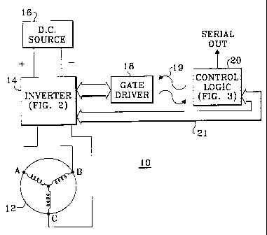
FIG. 1 is a block diagram of an exemplary embodiment of a three-phase,
voltage source inverter driven motor system 10 with which the present
invention may
be used. System 10 is illustrated as including a three-phase AC motor 12
driven by a
three-phase voltage source inverter 14 supplied by a DC power source 16. It
will be
recognized that the invention is applicable to a wide range of power converter-
load
configurations, for example, single phase converter and single phase motor;
multiple
motors in parallel driven by a single converter; transformer loads; and other
inductive
or resistive loads. Coupled to the inverter 14 is a gate driver module 18
which is
controlled by a control logic circuit 20. In operation, the inverter 14
converts the DC
power from DC source 16 into a three-phase excitation voltage for application
to
respective phase windings A, B and C of motor 12 in response to gate drive
signals
from gate driver module 18. The gate driver module 18 controls the switching
of the
inverter switching devices (i.e., GTOs) in the inverter 14 and is in turn
controlled by
the control logic circuit 20 via an optical control link 19 or other suitable
signal link.
In addition, feedback status signals from the GTO devices of the inverter 14
are
coupled back to the gate driver module 18 and to the control logic circuit 20
via the
optical link 19. Additional signals from current and voltage sensors of the
inverter 14
are coupled to the control logic circuit 20 via a bus 21, as shown. The
control logic
circuit 20 uses the feedback values from the optical link 19 and the sensed
current and
voltage values via the bus 21 to perform the predictive method of this
invention. In a
typical application, such as a commuter rail car, the inverter 14 may be
configured to
drive two motors in parallel and a single control circuit may control a total
of four
motors.
Referring now to FIG. 2, there is shown a detailed schematic diagram of a
three-phase inverter 14 including gate driver circuits 30a, 30b and 30c that
can benefit
JU1 1.3 U1 11:JOe! Dcu~SC u~ uw~ate uuwuua.. ..,, ~õ ,
. ~.. ~_ . _
z9
20-LC-2007
-5-
from the teachings of the present invention. As suggested above, inverter 14
comprises a first leg 25 (phase A) with an upper GTO 32 and a lower GTO 34
arranged in series with the anode of upper GTO 32 coupled to the positive DC
source
bus 33 and the cathode of the lower GTO 34 coupled to the negative DC source
bus
35. '1'he GTOs 32, 34 may typically be mounted on a heat sink with a
temperature
sensing thermal resistor (not shown) mounted thereon to detect overheating.
As will be understood by those skilled in the art, for each respective switch,
e.g., GTOs 32 and 34, there is a respective anti-parallel-diode 36 and 38
connected
from anode to cathode to provide a return path for inductive load currents. An
upper
inductor (LI) 40 (e.g., 5 micro H) and lower inductor (L2) 42 are coupled in
series
with the GTOs 32, 34. Also in series with the inductors L1, L2 are an upper
current
measurement circuit 44 (CM) (e.g., a Model LT1000-FI/SP45 Manufactured by LEM
of Switzerland) and a lower current measurement circuit 46 which are connected
at a
Phase A node 48, as shown. The node 48 is coupled to one phase (phase A) of
the
three-phase motor (or motors) 12 and, as shown, to a conventional high
impedance
voltage measurement circuit 50. The current measurement circuits 44, 46 thus
Maw generate current measurement signals lAP and IAN to be coupled to the
control logic
circuit 20 via bus 21 or to any suitable current monitor device. The current
measurement circuits may altemately be implenieuted with a single current
measurement circuit 45 coupled in series between the node 48 and the motor
phase A.
The voltage measurement circuit 50 (VM) generates a voltage measurement signal
VMA which is coupled to the control logic circuit 20 or to any suitable
voltage
monitor device.
A snubber circuit is also coupled to the phase A leg 25 and comprises a
capacitor 52 and diode 54 coupled across the GTO 32 and a capacitor 60 (e.g.,
3
micro F) and diode 58 coupled across the GTO 34, as shown. A resistor 56
(e.g., 0.25
ohms) provides a discharge path for snubber capacitors 52, 60.
Conventional high impedance voltage measurement circuits 62, 64 are coupled
respectively to the positive DC voltage source bus 33 and negative DC voltage
source
bus 35 to provide a positive voltage source measurement signal VDCP and a
negative
voltage source measuremeut signal VDCN.
~u~-~SI "'1'=
CA 02387916 2002-04-18
JUL 1.] U1 11 : Jt18 DQusstl Dr'[]Wr11CC DuWUua~o -ru.
~~~ ~~
~~1
~
20-LC-2007
-6-
The gate driver circuit 18a comprises an upper gate driver 70 and a lower gate
driver 72, each of which is coupled to the gate and cathode of the respective
GTO 32,
34, as shown. The gate drivers 70, 72 provide drive signals to the gates of
the GTOs
32, 34 to tum them on and off at the proper time. The gate drivers 70, 72 also
detect
whetlier the GTO actually did turn on or off in response to the signal (i.e.,
gate status
feedback). In addition, each gate driver 70, 72 is coupled to the control
logic circuit
20 via conventional optical couplers to pemiit input of gate command signals
t~ - (PMAIS, PMA2S) from the control logic circuit 20 on respective input
channels 76,
and to send gate status feedback signals (PMA1R, PMA2R), indicating whether
the
GTO is turned on or off, back to the control logic circuit 20 on respective
transmit
channels 78, 80.
The inverter power circuit 14 of FIG. 2 further comprises two additional legs
27, 29 (i.e., phase B, phase C), which are substantially identical to phase A
leg 25,
and, for the sake of simplicity and brevity of description, their operational
and circuit
details will not be repeated. The phase B leg 27 is connected to the AC motor
phase B
and the phase C leg 29 is connected to the AC motor phase C while the input
and
~# output optical lines and measurement signals are coupled to the control
logic circuit
as described with regard to the phase A leg 25.
FIG. 3 is a block diagram illustrating fiulher details of a control logic
circuit
20 20 of FIG. 1, and is made up of three main blocks: an input module 98, a
processor
-nwdule 100.and_an output module 102. The input module may include a
conventional
summing circuit 104 for phase A, a conventional summing circuit 106 for phase
B,
and an optional conventional summing circuit 108 for Phase C, each of which
combines the respective upper and lower current measurement values to obtain a
motor phase current value for the corresponding phase (i.e., IMTRA, IMTRB,
IMTRC). Since IMTRC can be derived as the sum of the currents of phases A and
B,
summing circuit 108 is optional. In addition, if the optional single current
measurement circuit 45 in the inverter 14 of FIG. 2 is used for each phase, no
summing circuits are needed. In each case, the motor phase current value may
be
coupled from the input module 98 to suitable analog to digital (A/D)
converters 110,
112 and optionally, to an A/D converter 114 in the output niodule 102. The A/D
AMMMW
CA 02387916 2002-04-18
CA 02387916 2002-04-18
WO 01/31770 PCTIUSOO/29125
-7-
converters 110, 112, 114 convert the motor phase current values to digital
form and
couple them through a standard cell 116 to a processor 120 via a bus 122, as
shown.
Alternatively, the digitized signals can be coupled directly to the processor
120 from
the A/D converters.
The input module also couples the voltage measurement values VMA, VMB,
VMC from the inverter 14 to respective summing circuits 124, 126, 128, along
with
the negative DC source voltage measurement signal VDCM, as shown.
These summing circuits thus provide voltage measurement values (VMA,
VMB, VMC) referenced to negative DC source bus 35 which are coupled to a
converter circuit 130. The converter circuit 130 converts the signals from
three-phase
signals (VA, VB, Vc) to two-phase signals (VD, VQ, VMS) which are coupled to
an A/D
converter 132 (e.g., a high speed, 12 bit A/D converter) of the processor
module 100,
as shown. Alternatively, the respective values of VA, VB, Vc values be coupled
directly to the A/D converter 132. The A/D converter 132 converts the input
values of
VA, VB, and Vc to digital form and couples the digitized values to a processor
120 via
a bus 134. The positive DC voltage bus measurement value VDCP from the
inverter
14 is also coupled to the input module 98 and is coupled to a summing circuit
136
along with the negative DC voltage bus value VDCN. The summing circuit 136
generates a voltage difference signal VL, representing the actual voltage
source line
voltage, which is also coupled to the A/D converter 132. The A/D converter 132
digitizes the value of VL and couples the digitized value to the processor
120, as
shown.
The processor 120 of the processor module 100 may be a single
microprocessor or it may be a dual processor architecture, such as
illustrated,
comprising an X processor 140 and a Y processor 142 both coupled to a dual
port
random access memory (RAM) 144. The processor 120 outputs signals via the bus
122 to the standard cell 116 of the output module 102 and communicates with
external devices such as an external processor or a display (e.g. for health
status
messages, reports on the values of the various voltages and/or currents, etc.)
via a
serial link 141. In addition, inputs from a port 146 are coupled to the
processor 120
from the output card 102. The processor 120 is controlled by a program stored
in each
CA 02387916 2002-04-18
WO 01/31770 PCT/US00/29125
-8-
PROM 145, 147 to process the input values from both the output module 102 and
the
input module 98 and generate output control signals coupled on the bus 122 to
the
standard cell 116 to control operation of the inverter-controlled motor system
10
during execution of the diagnostic techniques of the present invention.
The output module 102 may include a conventional optical receiver circuit
150 which receives the optical GTO status feedback signals (PMA1R, etc.) from
the
inverter driver module 18, and couples them in electrical form to a logic
buffer circuit
160 via a bus 152. These signals are also coupled to the processor 120 via the
port
146, as shown. In addition, gate firing pulses from the standard cell 116 are
coupled to
the logic buffer circuit 160 via a bus 154. The logic circuit 160 couples gate
pulses
(i.e., gate "on" or "off' command signals) to an optical driver 162 which
generates
optical gate command signals (PMA1S, etc.) which are coupled via the optical
channel to the inverter 14. In addition, the gate command signals from the
logic buffer
circuit 160 are coupled via a bus 164 to the processor 120 via the port 146,
as shown.
In normal operation, the control logic circuit 20 generates gate command
signals which are coupled to the gate driver module 18. The microprocessor 120
of
the module 100 controls generation of gate firing pulses by providing gate
firing
control signals to the standard cell 116 via the bus 122. The standard cell
116
generates gate firing control pulses in response to the gate firing control
signals from
the microprocessor 120. These gate firing control pulses are coupled to the
logic
buffer 160 via the bus 164 which couples gate command signals to the optical
driver
162 for transmission to the gate driver module 18. The GTOs of the inverter 14
are
then turned on and off by the gate driver module 18 at the appropriate times
under the
control of the gate command signals using technique well-understood in the
art.
Additionally, gate status feedback signals received from the optical receiver
150 are
coupled to the logic buffer 160 which utilizes them to determine if the GTOs
actually
switched, as commanded, in order to prevent unwanted conditions, such as
having
both upper and lower GTOs turned on at the same time.
FIG. 4 illustrates an exemplary flow chart 200 of various conditions during
which the voltage and current parameters may be monitored in order to detect
incipient failures in system 10 (FIG. 1). Upon start of diagnostics operations
at step
CA 02387916 2002-04-18
WO 01/31770 PCT/US00/29125
-9-
202, step 204 allows for ensuring that each GTO is in a respective
nonconductive
state. Step 206 allows for monitoring the respective values of the feedback
signals
when voltage buses 33 and 35 (FIG. 2) are set to substantially zero volts. As
suggested at step 208, each GTO may be turned on one at a time in order to
monitor
the respective gate status feedback signal (PMAIR, PMAZR, etc.) of each
respective
GTO.
Step 210 allows for monitoring the respective voltage and current parameters
when voltage buses 33 and 35 are set to a predetermined intermediate voltage
level
(e.g., 100 V) relative to the standard voltage normally supplied through
respective
buses 33 and 35. As suggested at 212, each voltage at junctions 48a, 48b and
48c
(FIG. 2) may be monitored as each respective GTO is turned on one at a time.
As
suggested at 214, respective currents flowing through at least two of the
motor phases
may be monitored either using the single current meter 45, or the combined
measurements from current meter 44 and 46 (FIG. 2) when two GTOs are
simultaneously turned on. It is noted that no two GTOs in a respective leg are
simultaneously turned on, since as explained above, this would electrically
short the
two respective voltage source buses to one another and could result in
substantial
damage to the power inverter system. As suggested at 216, an overcurrent
protection
test may be performed while three GTOs are simultaneously turned on subject to
the
same precaution above of not simultaneously turning on two GTOs in the same
leg.
Prior to return step 222, step 218 allows for monitoring the respective
voltage and
current parameters when voltage buses 33 and 35 are set to a relatively high
voltage
level (e.g., 400V). As suggested at 220, the monitoring of electrical
parameters at the
high voltage level may be performed while activating each GTO to a respective
conductive state one at a time, or the monitoring may be performed as
described in the
context of step 210 that allows for activation of more than one GTO at a time
provided no two GTOs are part of a common circuit leg.
FIGS. 5a and 5b illustrate operation of the inverter when one GTO is turned
on at a time and, in particular, FIG 5a illustrates inverter operation
including
associated voltage and current time plots when upper GTO 32 is activated in a
respective conductive state. Conversely, FIG 5b illustrates inverter operation
Jul 13 01 11:38a Beusse HroWnlee Houidoin 47(10 .5
S1
~JUg
~~A~J
~L
~A
20-LC-2007
-10-
including associated voltage and current time plots when lower GTO 34 is
activated
in a respective conductive state.
In each case, the respective electrical parameters that are monitored, e.g.,
voltage parameters VA, VB and VC; and peak current parameter Ipk may be
compcnsated or adjustcd for deviations from a nominal value due to
predetermined
external variables, such as ambient air temperature, baromctric pressure,
traction
motor states temperature, traction motor rotor temperature, motor RPM,
inverter air
flow, inverter age, expected variation from locomotive-to-locomotive, etc. It
will be
understood that the adjustment action may be executed either on the monitored
signals
constituting a first set of parameter values or nominal values constituting a
second set
of parametcr values since either of such sets of parameter values could be
adjusted
relative to the other to account for differences in operational and/or
environmental
conditions. The adjustment may be accomplished through the use of respective
transfer functions that may be experimentally or empirically derived. It will
be
appreciated that once an initial transfer function has been defined, suitable
adaptive
learning algorithms may be employed to fine tune the adjusting factors used in
the
transfcr function. By way of example and not of limitation, the transfer
function may
be of the form listed below:
Vcomp = Vraw *Kl * K2 . . . *Kn
wherein KI, K2 through Kn represent respective correcting factors, for each
extemal
variable, assuming a nuncber of n-external -variables, Vraw represents the raw
measurements or the uncompensated values of the monitored electrical
parameters
and Vcomp represents the compensated values of the electrical parameters. It
will be
appreciated that in the general case, Vcv = V19W f(Ki, K2 .,. Kõ) and
therefore the
transfer function need not be limited to the product of the correction
factors.
Once the monitored electrical parameters have been compensated, respective
tolerance bands may be defined so that any compensated values that fall within
a
predetermined tolerance band may be indicative of incipient failures in the
power
inverter system.
By way of example, a tolerance band could be defined based on the following
relationships for the monitored peak current lpk so that if Ipk > (I nominal +
a)/a,,
AVE!~ ~HM=
CA 02387916 2002-04-18
Jul 13 01 1 1: 38a Beusse liroiun 1 ee nowoo i n =ru ,
t~'tYtSQIJ / 2 91215
EFA~S 13 J U L 2001
20-LC-2007
-11-
or if lpk < (I nominal - a )/aõ then the occurrence of Ipk values that exceed
either of
the above inequalities would be indicative of an incipient failure. In the
above
equation a t may represent a first range limit and aõ may represent a
normalizing
factor. Similarly, a sccond range limit (e.g., a=) may be chosen beyond the
first range
limit so that values of Ipk outside that second range would be indicative of
unacceptable power inverter performance. In the foregoing example, Ipk values
within the first range limit would be indicative of satisfactory inverter
performance.
lpk values within the second and first range limits would be indicative of
incipient
failures and values exceeding the second range limit would be indicative of
unacceptable system performance. Thus, by suitably choosing the range limits
for
the compensated parameters, one may be able to detect failures at an early
stage, as
opposed to having to wait until a hard failure occurs. It will be appreciated
lhat hard
failures could result in a mission failure, such as train stoppage, whereas
detection of
an incipient failure would likely be pro-actively corrected without having to
suffer the
costly consequences associated with mission failures.
Fig. 6 illustrates operatian of the inverter when two GTOs, e.g., GTOs 32a and
32b (are simultaneously turned on in a respective conductive state. In this
case, it will
be appreciated from basic circuit theory that under normal operating
conditions IA
IB and thus if the magnitude of the respective phase currents are not
approximately
equal to one another and their difference exceeds a predetermined current
limit, (e.g.,
~ 15 amps) then 'the trser may declare an incipient failure. The ability to
detect
iiicipicnt failures becomes particularly powerful when used, not solely based
on
snapshots of the monitored paranieters, but used with a timeline of the values
of the
monitored parameters. The timeline would allow for detecting trends in the
monitored
parameters that may be associated with respective incipient failures. In
operation, the
techniques of the present invention allow for predicting incipient failures by
monitoring any trends in the monitored current parameters. It will be
appreciated that
the data monitored on-board each locomotive, that may be part of a large fleet
of
locomotives, may be transmittcd to a remote diagnostic service center where
dedicated analysis tools may be employed for aualyzing the monitored
parameters for
detection of incipient failures, as well as recommendations to timely correct
such
ai-~~ CA 02387916 2002-04-18
Jul 1i Ui 11 :jtla neusse tfrouWnlee nomooin
".'fiX 0 T/29125". .
ffAM 13 JUL 2001
2o-LC-2oo~
-12-
incipient failures. Further, the monitored data need not be limited to
electrical
parameters since fault log data may also be monitored so as to enhance the
predictive
accuracy of the detection techniques of the present invention.
Fig. 7 illustrates operation of the inverter when three GTO, e.g., GTOs 32a,
34b and 34c, are simultaneously turned on in a respective conductive state. In
this
case it will be appreciated that IA + IB + IC = 0 and thus if there is a
predeterTnined
non-zero current residual after summing the respective phase currents, then
depcnding
on the magnitude of such residual, the detection techniques of the present
invention
would allow for declaring either the presence of an incipient failure or the
presence of
unacceptable power converter performance. Conversely, if the value of the
monitored
electrical parameters are within an acceptable range, then one may conclude
that the
power inverter performance is acceptable.
It will be appreciated by those skilled in the art that during implementation
of
the algorithms for detecting incipient failures in the power inverter, the
motors are
stopped and the GTOs-are selectively turned on and off under control of the
processor
120 using the foregoing techniques. As suggested above, the processor may
include a
compensation module that allows for compensation of deviations in the
monitored
voltages and currents due to predetermined external parameters. The processor
then
analyzes the voltages and currents measured during the tcst scquence and
generates
appropriate alert or warning messages if an incipient failure or abnormality
is
detected.--As suggested above, the analysis of the monitored parameters need
not be
performed on-board the locomotive since the raw or compensated data could be
transmitted to a remote diagnostic service center using a suitable wireless
data
transceiver for analysis at the service center. It will be further appreciated
that such
service center may be configured to handle respective data downloads for
analysis
from a fleet of locomotives.
While the preferred embodiments of the present invention have been shown
and described herein, it will be obvious that such embodiments are provided by
way
of exarrmpte only. Numerous variations, changes and substitutions will occur
to those
of skill in the art without departing from the invention herein. Accordingly,
it is
AMMMSHEE1'
CA 02387916 2002-04-18
CA 02387916 2002-04-18
WO 01/31770 PCT/USOO/29125
-13-
intended that the invention be limited only by the spirit and scope of the
appended
claims.