Note: Descriptions are shown in the official language in which they were submitted.
CA 02388201 2002-04-19
WO 01/29759 PCT/GB00/04030
1
POSITION SENSOR
The present invention relates to a position sensor and to
parts therefor. The invention has particular although
not exclusive relevance to x-y digitising tablets which
operate with a cordless stylus. The invention is
particularly useful for embedding behind the display of
a hand-held electronic device such as a personal digital
assistant (PDA), mobile telephone, web browser or
products embodying combinations of these.
US Patent No. 4,878,533 discloses an x-y digitising
tablet which uses a resonant stylus. The digitising
tablet comprises a large number of overlapping, but
separate, loop coils which are arrayed in the x-y
direction. These loop coils are connected through a
switching circuit and a multiplexing circuit to an
excitation circuit and a receiving circuit. This system
is arranged so that the multiplexing circuit connects
each of the loop coils in sequence to the switching
circuit which firstly connects the connected loop coil to
the excitation circuit and then to the receiving circuit.
When a loop coil is connected to the excitation circuit,
a current is applied to the loop coil which energises the
resonant stylus. When the loop coil is connected to the
receiving circuit, the receiving circuit detects the
electromotive force (EMF) induced in the connected loop
coil by the resonant stylus. This system identifies the
current position of the stylus by detecting the loop coil
which provides the greatest output signal level.
A problem with the digitising tablet described in US
Patent No. 4,878,533 is that it consumes a large amount
of power in order to energise and detect the signals in
each of the loop coils, which makes it unsuitable for
CA 02388201 2002-04-19
WO 01/29759 PCT/GB00/04030
2
hand-held battery-powered devices such as PDAs and mobile
telephones.
An aim of the present invention is to provide components
for use in an alternative form of position sensor in
which a magnetic field is generated and coupled to a
resonant stylus.
According to one aspect of the invention, there is
provided a position detector in which a series of
excitation pulses is applied across an excitation winding
with the duration of the excitation pulses being less
than a decay time of a current loop incorporating the
excitation winding. The long decay time enables current
to flow in the excitation winding for a significant
amount of time after each excitation pulse which means
that shorter excitation pulses can be used thereby
drawing less power from the power supply.
According to another aspect of the invention, there is
provided a position detector in which' a number of
excitation sequences are applied across an excitation
winding, each excitation sequence comprising a series of
excitation pulses whose durations have been arranged to
reduce any slowly-varying components in the excitation
sequence. By reducing the slowly-varying components, the
power drawn from the power supply is reduced.
Various features and aspects of the present invention
will become apparent from the following description of
exemplary embodiments which are described with reference
to the accompanying drawings in which:
Figure 1 is a schematic view of a hand-held personal
digital assistant (PDA) which includes an x-y digitising
CA 02388201 2002-04-19
WO 01/29759 PCT/GB00/04030
3
system located behind the PDA's liquid crystal display
which can sense the (x, y) position of a resonant stylus;
Figure 2 schematically illustrates a cross-sectional view
of the personal digital assistant shown in Figure 1,
illustrating the positional relationship between a sensor
printed circuit board of the digitising system and the
liquid crystal display;
Figure 3 is a schematic functional block diagram
illustrating the excitation and processing electronics of
the x-y digitising system and illustrating the magnetic
coupling between an excitation winding of the digitising
system and the resonant stylus and the magnetic coupling
between the resonant stylus and four sensor windings
which form part of the digitising system;
Figure 4a schematically illustrates an approximation of
the way in which the peak amplitude of the signals
induced in x-sensor windings of the digitising system
vary with the x-coordinate of the position of the stylus
relative to the liquid crystal display;
Figure 4b schematically illustrates an approximation of
the way in which the peak amplitude of the signals
induced in y-sensor windings of the digitising system
vary with the y-coordinate of the position of the stylus
relative to the liquid crystal display;
Figure 5a illustrates the form of the excitation winding
of the digitising system which forms part of the personal
digital assistant shown in Figure 1;
Figure 5b illustrates the form of a sin x sensor winding
of the digitising system which forms part of the personal
CA 02388201 2002-04-19
WO 01/29759 PCT/GB00/04030
4
digital assistant shown in Figure 1;
Figure 5c illustrates the form of a cos x sensor winding
of the digitising system which forms part of the personal
digital assistant shown in Figure 1;
Figure 5d illustrates the form of a sin y sensor winding
of the digitising system which forms part of the personal
digital assistant shown in Figure 1;
Figure 5e illustrates the form of a cos y sensor winding
of the digitising system which forms part of the personal
digital assistant shown in Figure 1;
Figure 5f shows a top layer of a printed circuit board
which carries the windings shown in Figures 5a to 5e;
Figure 5g shows a bottom layer of the printed circuit
board which carries the windings shown in Figures 5a to
5e;
Figure 6 is a cross-sectional view of the resonant stylus
shown in Figure 1;
Figure 7 is a schematic block diagram showing the form of
a digital processing and signal generation unit which
forms part of the excitation and processing circuitry
shown in Figure 3;
Figure 8 is a circuit diagram illustrating in more detail
the form of an excitation driver which forms part of the
excitation and processing circuitry shown in Figure 3;
Figure 9a is a timing diagram illustrating the form of an
excitation voltage applied to the excitation winding by
CA 02388201 2002-04-19
WO 01/29759 PCT/GB00/04030
the excitation and processing electronics shown in Figure
3 for a first example;
Figure 9b is a timing diagram illustrating the form of
5 the excitation current flowing through the excitation
winding as a result of the applied excitation voltage
shown in Figure 9a;
Figure 9c is a timing diagram illustrating the form of
the current drawn from the power supply in order to
generate the excitation voltage shown in Figure 9a;
Figure 9d is a timing diagram illustrating the form of an
electromotive force induced in a sensor winding by the
resonant stylus when the excitation voltage shown in
Figure 9a is applied to the excitation winding;
Figure 10a is a timing diagram illustrating the form of
an excitation voltage applied to the excitation winding
by the excitation and processing electronics shown in
Figure 3 for a third example;
Figure lOb is a timing diagram illustrating the form of
the excitation current flowing through the excitation
winding as a result of the applied excitation winding
shown in Figure 10a;
Figure lOc is a timing diagram illustrating the form of
the current drawn from the power supply in order to
generate the excitation voltage shown in Figure 10a;
Figure lOd is a timing diagram illustrating the form of
an electromotive force induced in a sensor winding by the
resonant stylus when the excitation voltage shown in
Figure 10a is applied to the excitation winding;
CA 02388201 2002-04-19
WO 01/29759 PCT/GB00/04030
6
Figure lla is a timing diagram illustrating the form of
the end of the excitation sequence applied to the
excitation winding by the excitation and processing
electronics shown in Figure 3 for a fourth example;
Figure llb is a timing diagram illustrating the form of
the excitation current flowing through the excitation
winding as a result of the applied excitation voltage
shown in Figure 11a;
Figure llc is a timing diagram illustrating the form of
the current drawn from the power supply in order to
generate the excitation voltage shown in Figure 11a;
Figure lld is a timing diagram illustrating the form of
an electromotive force induced in a sensor winding by the
resonant stylus when the excitation voltage shown in
Figure lla is applied to the excitation winding;
Figure 12a is a timing diagram illustrating the end of an
excitation voltage sequence applied by the excitation and
processing electronics shown in Figure 3 for a fifth
example;
Figure 12b is a timing diagram illustrating the form of
the excitation current flowing through the excitation
winding as a result of the applied excitation voltage
shown in Figure 12a;
Figure 12c is a timing diagram illustrating the form of
the current drawn from the power supply in order to
generate the excitation voltage shown in Figure 12a;
Figure 12d is a timing diagram illustrating the form of
an electromotive force induced in a sensor winding by the
CA 02388201 2002-04-19
WO 01/29759 PCT/GB00/04030
7
resonant stylus when the excitation voltage shown in
Figure 12a is applied to the excitation winding;
Figure 13a is a timing diagram illustrating the form of
an excitation voltage sequence applied by the excitation
winding of excitation and processing electronics shown in
Figure 3 for a sixth example;
Figure 13b is a timing diagram illustrating the form of
the excitation current flowing the excitation winding as
a result of the applied excitation voltage shown in
Figure 13a;
Figure l3c.is a timing diagram illustrating the form of
the current drawn from the power supply in order to
generate the excitation voltage shown in Figure 13a;
Figure 13d is a timing diagram illustrating the form of
an electromotive force induced in a sensor winding by the
resonant stylus when the excitation voltage shown in
Figure 13a is applied to the excitation winding;
Figure 14a is a timing diagram illustrating the form of
an excitation voltage sequence applied by the excitation
winding of the excitation and processing electronics
shown in Figure 3 in a seventh example;
Figure 14b is a timing diagram illustrating the form of
the excitation current flowing through the excitation
winding as a result of the applied excitation voltage
shown in Figure 14a;
Figure 14c is a timing diagram illustrating the form of
the current drawn from the power supply in order to
generate the excitation voltage shown in Figure 14a;
CA 02388201 2002-04-19
WO 01/29759 PCT/GB00/04030
8
Figure 14d is a timing diagram illustrating the form of
an electromotive force induced in a sensor winding by the
resonant stylus when the excitation voltage shown in
Figure 14a is applied to the excitation winding;
Figure 15a is a timing diagram illustrating the form of
an excitation voltage applied by the excitation winding
of the excitation and processing electronic shown in
Figure 3 in an eighth example;
Figure 15b is a timing diagram illustrating the form of
the excitation current flowing through the excitation
winding as a result of the applied excitation voltage
shown in Figure 15a;
Figure 15c is a timing diagram illustrating the form of
the current drawn from the power supply in order to
generate the excitation voltage shown in Figure 15a;
Figure 15d is a timing diagram illustrating the form of
an electromotive force induced in a sensor winding by the
resonant stylus when the excitation voltage shown in
Figure 15a is applied to the excitation winding;
Figure 16 is a circuit diagram illustrating an
alternative form of the excitation driver of the
excitation and processing circuitry shown in Figure 3;
Figure 17a is a timing diagram illustrating the form of
an excitation voltage sequence applied by the excitation
winding of the excitation and processing electronics
shown in Figure 3 in a ninth example;
Figure 17b is a timing diagram illustrating the form of
the excitation current flowing through the excitation
CA 02388201 2002-04-19
WO 01/29759 PCT/GB00/04030
9
winding as a result of the applied excitation voltage
shown in Figure 17a;
Figure 17c is a timing diagram illustrating the form of
the current drawn from the power supply in order to
generate the excitation voltage shown in Figure 17a;
Figure 17d is a timing diagram illustrating the form of
an electromotive force induced in a sensor winding by the
resonant stylus when the excitation voltage shown in
Figure 17a is applied to the excitation winding;
Figure 18a is timing diagram illustrating the form of an
excitation voltage sequence applied by the excitation
winding of the excitation and processing electronics
shown in Figure 3 in a tenth example;
Figure 18b is a timing diagram illustrating the form of
the excitation current flowing through the excitation
winding as a result of the applied excitation voltage
shown in Figure 18a;
Figure 18c is a timing diagram illustrating the form of
the current drawn from the power supply in order to
generate the excitation voltage shown in Figure 18a;
Figure 18d is a timing diagram illustrating the form of
an electromotive force induced in a sensor winding by the
resonant stylus when the excitation voltage shown in
Figure 18a is applied to the excitation winding;
Figure 19a is a timing diagram illustrating the form of
an excitation voltage sequence applied by the excitation
winding of the excitation and processing electronics
shown in Figure 3 in an eleventh example;
CA 02388201 2002-04-19
WO 01/29759 PCT/GB00/04030
Figure 19b is timing diagram illustrating the form of the
excitation current flowing through the excitation winding
as a result of the applied excitation voltage shown in
Figure 19a;
5
Figure 19c is a timing diagram illustrating the form of
the current drawn from the power supply in order to
generate the excitation voltage shown in Figure 19a;
10 Figure 19d is a timing diagram illustrating the form of
an electromotive force induced in ~a sensor winding by the
resonant stylus when the excitation voltage shown in
Figure 19a is applied to the excitation winding; and
Figure 20 is a perspective view showing a mobile
telephone having a liquid crystal display and a
digitising system under the display which is operable to
sense the position of a resonant stylus relative to the
display.
Overview of Digitising System
Figure 1 shows a hand-held personal digital assistant
(PDA) 1 which employs an x-y digitising system (not
shown) which is located beneath a liquid crystal display
3 of the PDA 1. The x-y digitising system is operable to
detect the presence and x-y position of a resonant stylus
5 relative to the LCD 3. The position signals output
from the digitising system are used by the PDA 1 to
control information that is displayed on the LCD 3 and to
control the operating function of the PDA 1. As shown,
the PDA 1 also includes a number of push buttons beneath
the LCD 3 including an on-off button 7 and a number of
control buttons 9-1 to 9-4 which are used to control
different functions of the PDA 1.
CA 02388201 2002-04-19
WO 01/29759 PCT/GB00/04030
11
Figure 2 shows a crass-sectional view on A-A of the PDA
1 shown in Figure 1. As shown, the PDA 1 includes a
liquid crystal display 3 which, in this embodiment, is
between 1.5mm and 3mm thick. Beneath the LCD 3, there is
an electroluminescent backlight 11 for providing a
backlight for the LCD 3. In this embodiment, this
backlight layer 11 has a thickness of approximately
150~m. Beneath these layers, there is a 0.2mm thick
sensor printed circuit board (PCB) 13 which. forms part of
the above-mentioned x-y digitising system. This sensor
PCB 13 carries the excitation winding and the sensor
windings used for sending signals to and receiving
signals from the resonant stylus 5. Beneath the sensor
PCB 13 there is a printed circuit board 15 which carries
the electronics for controlling the functions of the PDA
and the digitiser electronics for processing the signals
received from and controlling the signals sent to the
windings on the sensor PCB 13.
As shown in Figure 2, in this embodiment, a .grounded
electrostatic screen 17 is provided between the sensor
printed circuit board 13 and the electroluminescent
backlight 11 in order to reduce noise from the liquid
crystal display 3 and the backlight 11 from interfering
with the x-y digitising system. In this embodiment, this
electrostatic screen is formed from a continuous layer of
carbon ink which is approximately l0~cm thick and has a
relatively high surface resistivity (e.g. > 1 ohm per
square) so that it does not interfere with the magnetic
sensing function. Further, as shown in Figure 2, beneath
the sensor PCB 13 is a 50/.cm layer of pressure sensitive
adhesive 19 for bonding the sensor PCB 13 onto a magnetic
screen 21, which in this embodiment is a 25um layer of
spin melt ribbon (for example Vitrovac 6025 manufactured
by Vacuumschmelze, Hanau, Germany). As those skilled in
CA 02388201 2002-04-19
WO 01/29759 PCT/GB00/04030
12
the art will appreciate, the magnetic screen 21 is
provided in order to reduce any disturbance which may be
caused to the x-y digitising system by, for example, the
electronics behind the sensor PCB 13. It also enhances
the sensitivity of the x-y digitising system since it
provides a permeable path for magnetic flux to pass
behind the sensor windings on the sensor PCB 13. As
shown in Figure 2, encasing these layers and providing
mechanical support is an outer casing 23 which is made,
in this embodiment, from plastic.
Figure 3 schematically illustrates a functional block
diagram of the digitising system which forms part of the
PDA shown in Figure 1. Figure 3 also illustrates the way
in which the excitation winding and the sensor windings
interact with the resonant stylus 5. In particular,
Figure 3 schematically shows an excitation winding 29,
two x-sensor windings 31 and 33 for sensing x position
and two y-sensor windings 35 and 37 for sensing y
position. Each of these windings is formed by printed
conductors on the sensor PCB 13. As will be explained in
more detail below, the sensor windings 31, 33, 35 and 37
are periodic and are in spatial phase quadrature relative
to each other. Therefore, in the following description
x-sensor winding 31 will be referred to as the sin x
sensor winding, x-sensor winding 33 will be referred to
as the cos x sensor winding, y-sensor winding 35 will be
referred to as the sin y sensor winding and y-sensor
winding 37 will be referred to as the cos y sensor
winding. As illustrated by the arrows 39, these windings
are operable, in use, to couple magnetically with a
resonant circuit 41 (comprising a capacitor 43 and an
inductor coil 45) in the resonant stylus 5.
The excitation winding and the sensor windings are
CA 02388201 2002-04-19
WO 01/29759 PCT/GB00/04030
13
connected to digitiser electronics 49 (indicated by the
dashed block in Figure 3) which generates an excitation
signal which passes through the excitation winding 29 and
determines an x-y position of the resonant stylus 5 from
signals received from the sensor windings. The digitiser
electronics 49 includes a digital processing and signal
generation unit 59 which, in operation, generates control
signals TXA and TXB for controlling an excitation driver
51 which applies an excitation voltage across the ends of
the excitation winding 29. In this embodiment, the
excitation voltage applied across the ends of the
excitation winding 29 comprises a sequence of positive
and negative pulses having a fundamental frequency
component (Fo) of approximately 100kHz, which is matched
to the resonant frequency of the resonant circuit 41.
Various alternative excitation sequences will be
described in more detail hereinafter.
The excitation current flowing in the excitation winding
29 generates a corresponding electromagnetic field which
magnetically couples, as indicated by the arrow 39-1,
with the resonant circuit 41 and causes it to resonate.
In this embodiment, the excitation winding 29 is arranged
to keep the magnetic coupling between it and the
resonator as constant as possible with the x-y position
of the stylus relative to the LCD 3. When the resonator
41 is resonating, it generates its own electromagnetic
field which magnetically couples, as represented by the
arrows 39-2, 39-3, 39-4 and 39-5, with the sensor
windings 31, 33, 35 and 37 respectively. As will be
explained in more detail below, the sensor windings 31,
33, 35 and 37 are designed so that the coupling between
them and the resonant stylus varies with the x or y
position of the stylus and so that there is minimum
direct coupling between them and the excitation winding
CA 02388201 2002-04-19
WO 01/29759 PCT/GB00/04030
14
29. Therefore, the signal received in the sensor
windings should only vary with the magnetic coupling
between the resonator 41 and the respective sensor
winding. Consequently, by suitable processing of the
signals received in the sensor windings, the x-y position
of the resonator 41, and hence of the resonant stylus 5,
can be determined relative to the sensor windings.
In this embodiment, in order to reduce the effect of any
breakthrough from the excitation winding 29 to the sensor
windings on the x-y position measurement, the excitation
current is not continuously applied to the excitation
winding 29 but instead bursts of the excitation current
are applied, and the signals induced in the sensor
windings are only detected between the bursts of the
excitation current. This mode of operation is referred
to as pulse echo and works because the resonator 41
continues to resonate after the burst of excitation
current has ended.
As mentioned above, the sensor windings are periodic and
are in spatial phase quadrature. Therefore, the four
signals induced in the four sensor windings from the
resonant circuit 41 can be approximated by:
E31 = Ae -riz si ~ x cos[2~F t + o ] ( 1 )
x
E33 = Ae -l~T cos 2~x cos[2~tF t + ra] ( 2 )
L
E35 = Ae -r~~ si ~ y cos[2~F t + a~] ( 3 )
Y
E3~ = Ae -'~'cos ~y cos[2~F t+o] ( 4 )
Y
CA 02388201 2002-04-19
WO 01/29759 PCT/GB00/04030
where A is a coupling coefficient which depends upon,
among other things, the distance of the stylus from the
windings and the number of turns in the sensor windings;
x is the x-position of the resonant stylus relative to
5 the sensor windings; y is the y-position of the resonant
stylus relative to the sensor windings; Lx is a spatial
wavelength of the sensor windings in the x-direction and
is typically slightly greater than the width of the board
in the x-direction (and in this embodiment is 70mm); Ly
10 is a spatial wavelength of the sensor windings in the y-
direction and is typically slighter greater than the
width of the board in the y-direction (and in this
embodiment is 50mm) ; e-t~' is the exponential decay of the
resonator signal after the burst of excitation signal has
15 ended, with i being a resonator constant which is equal
to the quality factor of the resonant circuit 41 divided
by the product of pi (n) and the resonant frequency of
the resonant circuit 41; and m is an electrical phase
shift caused by a difference between the fundamental
frequency of the excitation current and the resonant
frequency of the resonator 41. In this embodiment, the
resonant stylus 5 is designed so that its resonant
frequency changes with the pressure applied to the tip of
the stylus. This change in frequency causes a change in
the phase shift a and therefore by measuring the phase
shift m it can be determined whether or not the tip of
the resonant stylus 5 is pressed into contact with the
LCD 3.
As can be seen from equations (1) to (4), the peak
amplitude of the signals induced in the sensor windings
vary as the sin or cos of either the x or y position.
This is illustrated in Figures 4a and 4b. In particular,
Figure 4a illustrates the way in which the peak amplitude
of the signal induced in sensor winding 31 and the way in
CA 02388201 2002-04-19
WO 01/29759 PCT/GB00/04030
16
which the signal induced in sensor winding 33 varies with
the x-position of the resonant stylus relative to the
sensor windings and Figure 4b shows the way in which the
peak amplitude of the signals induced in sensor winding
35 and sensor winding 37 vary with the y-position of the
resonant stylus relative to the sensor windings. As
shown in Figure 4, the pitch (Lx) of the windings in the
x-direction is greater than the pitch (LY) of the
windings in the y-direction. This is because, in this
embodiment, the measurement area is rectangular.
Therefore, as those skilled in the art will appreciate,
both the x-y position information of the resonant stylus
5 and the phase shift v~ can be determined from the
signals induced in the sensor windings by suitable
demodulation and processing. As shown in Figure 3, this
demodulation is achieved by connecting each of the four
sensor windings to a respective two of the eight mixers
69-1 to 69-8, where for each sensor winding the induced
signal is multiplied by a square wave at the same
frequency as and in phase with the excitation current in
one of the respective mixers and is multiplied by a
square wave signal at the same frequency as and 90° out
of phase with the excitation current in the other of the
respective mixers. This generates an in phase (I)
component and a quadrature phase ( Q ) component of each of
the demodulated signals. In this embodiment, the in
phase components of the demodulated signals from all the
sensor windings are used to determine the position
information and the in phase and quadrature phase
components of the demodulated signal from one of the
sensor windings are used to determine the electrical
phase shift (i.e. o). As shown in Figure 3, the output
from each mixer 69-1 to 69-8 is input to a respective
integrator 71-1 to 71-8 which, after being reset,
CA 02388201 2002-04-19
WO 01/29759 PCT/GB00/04030
17
integrates the output from the mixer over a time period
which is a multiple of 1/Fo (in order to reduce the
effect of error signals from the mixer at the fundamental
frequency, for example clock feed-through). The
following equations approximate the outputs from the
integrators 71-1 to 71-4:
sin x 1 = A1 sin ~ x cosra ( 5 )
x
sin x_Q = A1 sin 2~x sinm ( 6 )
L
x
cos x I = A1 cos ~ x cosm ( 7 )
x
cos_x_Q = A1 cos ~ x sino ( 8 )
x
where A, is a constant which varies with, among other
things, the constant A, the resonator constant i and the
integration period. Similar signals are obtained from
integrators 71-5 to 71-8, except these vary with the y-
position rather than with the x-position.
As shown in Figure 3, the outputs from the integrators 71
are input to an analogue-to-digital converter 73 where
they are converted into digital signals which are input
to the digital processing and signal generation unit 59
via the A to D interface unit 75. The digital processing
and signal generation unit 59 then performs an arc
tangent function ( atan 2 ) on the ratio of the sin x-I
signal and the cos x-I signal to determine the x-position
of the resonant stylus and similarly performs an arc
tangent function on the ratio of the sin y-I signal and
the cos y-I to determine the y-position of the resonant
CA 02388201 2002-04-19
WO 01/29759 PCT/GB00/04030
18
stylus 5. The digital processing and signal generation
unit 59 also calculates an arc tangent function on the
ratio of the quadrature phase component to the in phase
component of the signals from one of the sensor windings,
in order to determine the phase angle e~.
As shown in Figure 3, both the in phase (I) and
quadrature phase (Q) components of the signal induced in
each of the sensor windings are measured. This is
because, at certain x and y positions, the ratio of the
in phase and quadrature phase components from the sensor
windings will not be reliable. This occurs when the sin
or cos position components are approximately zero.
Therefore, in this embodiment, the digital processing and
signal generation unit 59 determines the phase angle m
using a weighted combination of the in phase and
quadrature phase signals from both the sin and cos
windings, where the weighting used varies in dependence
upon the determined x and y position of the stylus.
After the digital processing and signal generation unit
59 has determined the current x-y position of the
resonant stylus and determined whether or not the stylus
has been brought into contact with the LCD 3, it outputs
this information to the PDA electronics through the
interface unit 77. This information is then used by the
PDA electronics to control information displayed on the
LCD 3 and the PDA's mode of function. In this
embodiment, the excitation and position determining
circuitry 49 performs the above calculations five hundred
times per second.
A brief description has been given above of the way in
which the digitiser system of the present embodiment
determines the x-y position of the resonant stylus
CA 02388201 2002-04-19
WO 01/29759 PCT/GB00/04030
19
relative to the sensor windings. The particular form of
excitation and sensor windings used and the particular
resonant stylus, digital processing and excitation
signals used in this embodiment will now be described in
more detail.
Digitiser Windings
Figure 5a illustrates the form of the excitation winding
29 used in this embodiment. The winding 29 is formed by
five turns of rectangular conductor on each side of the
sensor PCB 13 which are connected in series at through
holes or vias, some of which are labelled 97. In Figure
5a, the conductors on the top layer of the sensor PCB 13
are shown as solid lines whilst those on the bottom layer
of the sensor PCB are shown as broken lines. Figure 5a
also shows the two connection pads 101 and 103 used to
connect the ends of the excitation winding 29 to the
excitation driver 51. In this embodiment, the excitation
winding 29 is wound around the outside of the sensor
windings (not shown).
Figure 5b shows the printed conductors which form the sin
x sensor winding 31. Again, the printed conductors on
the top layer of the sensor PCB 13 are shown as solid
lines whilst those on the bottom layer are shown as
dashed lines. As shown, the conductor tracks which
extend substantially in the y-direction are provided on
the top layer of the sensor PCB 13 and those which extend
substantially in the x-direction are provided on the
bottom layer of the sensor PCB 13 and the ends of the
conductor tracks on the top layer are connected to the
ends of the conductor tracks on the bottom layer at the
via holes, some of which are labelled 97. Figure 5b also
shows the two connection pads 105 and 107 which are
provided for connecting the sin x sensor winding 31 to
CA 02388201 2002-04-19
WO 01/29759 PCT/GB00/04030
the digitiser electronics.
As shown, the conductor tracks of the sin x sensor
winding 31 are connected to form two sets of loops 32-1
5 and 32-2 which are arranged in succession along the x-
direction. As those skilled in the art will appreciate,
if a point magnetic field source (or something similar
such as the resonant stylus) is moved across the sensor
winding 31, then the magnetic coupling between the point
10 source and the sensor winding 31 will vary approximately
sinusoidally with the x-position of the point source.
There will be little or no variation with the y-position.
Figure 5c shows the printed conductors which form the cos
15 x sensor winding 33. Again, the printed conductors on
the top layer of the sensor PCB 13 are shown as solid
lines whilst those on the bottom layer are shown as
dashed lines. Figure 5c also shows the two connection
pads 109 and 111 which are provided for connecting the
20 cos x sensor winding 33 to the digitiser electronics. As
shown, the conductor tracks of the cos x sensor winding
33 are connected to form three sets of loops 34-la, 34-2
and 34-lb which are arranged in succession along the x-
direction.
As with the sin x sensor winding, when the resonant
stylus 5 is moved across the sensor winding 33, the
magnetic coupling between the resonant stylus 5 and the
cos x sensor winding 33 varies approximately sinusoidally
with the x-position of the stylus 5. However, since the
sets of loops of the cos x sensor winding 33 are shifted
in the x-direction by a quarter of the winding pitch
(LX), the sinusoidal variation will be in phase
quadrature to the variation of the sin x sensor winding
31. As a result, the signal induced in the sensor
CA 02388201 2002-04-19
WO 01/29759 PCT/GB00/04030
21
winding 33 by the resonant stylus 5 has a peak amplitude
which approximately varies as the cosine of the x-
position of the stylus 5.
Figures 5d and 5e show the printed conductors which form
the sin y sensor winding 35 and the cos y sensor winding
37. As shown in these figures, these sensor windings are
similar to the sin x and cos x sensor windings except
they are rotated through 90°. As shown in Figures Sd and
5e, the sin y sensor winding 35 shares the connection pad
107 with the sin x sensor winding ~ 31 and the cos y sensor
winding 37 shares the connection pad 111 with the cos.x
sensor winding 33. Figure 5f shows the top layer of
printed conductors and Figure 5g shows the bottom layer
of printed conductors of the sensor PCB 13 which together
form the excitation winding 29 and the sensor windings
31, 33, 35 and 37.
Stylus
Figure 6 shows the resonant stylus 5 used in this
embodiment in cross-section. As shown, the stylus
comprises a hollow front body portion 152 and a hollow
rear body portion 154 which house: the resonant circuit
comprising the inductor coil 45 and the capacitor 43 ( not
shown); a 2mm diameter ferrite rod 153; a first movement-
limiting member 155; a second movement-limiting member
157; a nib 159; and a spring 163.
A more detailed description and explanation of the layout
of the excitation and sensor windings and of the stylus
used in this embodiment can be found in International
Patent Application No. PCT/GB99/03989, the whole contents
of which are hereby incorporated by reference.
CA 02388201 2002-04-19
WO 01/29759 PCT/GB00/04030
22
Digital Processing and Signal Generation Unit
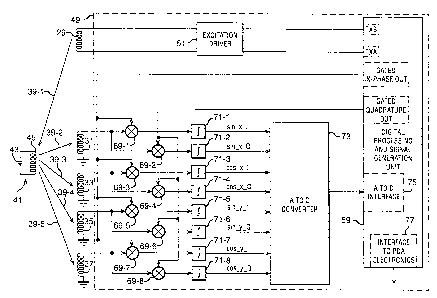
As shown schematically in Figure 7, the digital
processing and signal generating unit 59 includes an
interface unit 77 via which a processor 171 in the
digital processing and signal generation unit 59
communicates with a processor (not shown) which controls
the PDA electronics, allowing system set-up information
to be transmitted from the PDA processor to the processor
171 and the x-y position of the resonant stylus 5 on the
LCD 3 to be transmitted from the processor 171 to the PDA
processor. The processor 171 is also connected to a read
only memory (ROM) 173, which stores control procedures
(such as initialisation routines) and a random access
memory (RAM) 175 which provides working space for the
digital signal processing.
The processor 171 sends control parameters to a digital
waveform generator 179 which, in accordance with the
control parameters, generates the control signals TXA and
TXB for the excitation driver 51 and the in-phase and
quadrature-phase mixing signals for the mixers 69-1 to
69-8. In this embodiment, the digital waveform generator
179 is software-based with the timings at which TXA, TXB,
in-phase out and quadrature out are switched between a +1
state, a -1 state and a 0 state being determined using
the control parameters sent by the processor 171. An
analog to digital interface 181 receives the digital
signals from the analog to digital converter 73 and
transfers them to the processor 171 where they are
processed to obtain the x-position and the y-position of
the stylus and the phase information (m) for the stylus
as described above.
Excitation Driver
Figure 8 shows a circuit diagram of the excitation driver
CA 02388201 2002-04-19
WO 01/29759 PCT/GB00/04030
23
51 employed in this embodiment. As shown, the excitation
driver 51 comprises two amplification circuits 191-1 and
191-2 which are connected in parallel between the supply
voltage V~~ and ground. A supply resistance Re"P and a
supply capacitance Cg"p are included to minimise the
ripple current introduced into the supply rails by the
operation of the excitation circuit. The amplification
circuit 191-1 comprises a p-channel MOSFET switch P1 and
a n-channel MOSFET switch N1 with the drain of P1
connected to the drain of N1 and the gates of P1 and N1
connected to each other. The amplification circuit 191-1
has an input terminal 193-1, located at the common gate
of P1 and N1, to which the drive signal TXA is applied
and an output terminal 195-1, located at the connection
between the drain of P1 and the drain of N1, which is
connected to the connection pad 101 of the excitation
winding 29. Amplification circuit 191-2 is formed in an
identical manner to amplification circuit 191-2 using a
p-channel MOSFET switch PZ and a n-channel MOSFET switch
NZ and the drive signal TXB is applied to the input
terminal 193-2 of the amplification circuit 191-2, and
the output terminal 195-2 of the amplification circuit
191-2 is connected to the connection pad 103 of the
excitation winding 29. In this embodiment low resistance
MOSFET switches are used.
The excitation voltage applied across the excitation
winding 29 is the voltage between the output terminals
195-1 and 195-2 of the amplification circuits 191-1 and
191-2 respectively and will therefore vary according to
the drive signals TXA and TXB as indicated in table 1.
CA 02388201 2002-04-19
WO 01/29759 PCT/GB00/04030
24
TXA TXB EXCITATION VOLTAGE (V)
0 0 0
0 1 +Vcc
1 0 -Vcc
1 1 0
Table 1: Variation of excitation voltage with TXA and
TXB.
Excitation Signals
The performance of the x-y digitising system illustrated
in Figure 3 will now be discussed for a number of
exemplary excitation signals. The performance is
assessed by considering computer simulations of the
performance in which the effect of RS"P and CS"P has been
assumed to be negligible. Although this assumption is
not necessarily true in practice, the conclusions derived
from these computer simulations are still valid and have
been verified experimentally. For all the examples, the
resonant circuit 41 has a resonant frequency of 100kHz
and a quality factor of 40 and the excitation sequence is
repeated at a frequency of 500Hz. However, a number of
parameters are varied in the examples, in particular the
inductance LeX and the AC resistance at 100kHz ReX of the
excitation winding 29, the resistance R" of the n-channel
MOSFET switches and the resistance -RP of the p-channel
MOSFET switches.
Example 1
In example 1, Lex is 25uH, ReX is 10 ohms, Rn is 1 ohm and
Rp is 3 ohms. Figure 9a shows the excitation voltage
which is applied across the excitation winding 29 in this
example for a single excitation sequence. As shown, the
CA 02388201 2002-04-19
WO 01/29759 PCT/GB00/04030
excitation sequence comprises a series of alternating
positive and negative pulses which, unlike a conventional
excitation sequence which is a square wave, have periods
between the pulses during which the excitation voltage is
5 returned to zero. The fundamental frequency of the
excitation sequence is 100 kHz, corresponding to a
fundamental excitation period of lONs, with the duration
of each pulse, apart from the first and last positive
pulses, set to 0.75~s and with each of the pulses being
10 separated by a period of 4.25us. Therefore, for the
middle pulses, the ratio of the time in the fundamental
excitation period during which either a positive or
negative pulse is applied to the excitation winding to
the duration of the fundamental period, which will
15 hereinafter be referred to as the middle-pulse-ratio, is
0.15. In this embodiment the supply applies an EMF of
3.3V across the ends of the excitation winding 29, which
is a typical value for a battery-powered device.
20 Figure 9b shows a timing diagram for the form of the
excitation current, that is the current flowing through
the excitation winding 29, as a result of the excitation
voltage shown in Figure 9a being applied across the
excitation winding. As shown, the excitation current
25 reaches a peak value when the excitation pulses are
applied and then decays exponentially when the excitation
voltage is set equal to zero. This exponential decay is
caused because even with no EMF applied across the
excitation winding 29, current can continue to flow due
to a back EMF of the excitation winding 29 caused by the
winding's inductance LeX. In practice, the excitation
current may initially decay more rapidly than shown in
Figure 9b due to AC losses for the excitation coil which
may arise, for example, if the excitation coil couples
with any metal forming part of the PDA 1. However, this
CA 02388201 2002-04-19
WO 01/29759 PCT/GB00/04030
26
does not effect the conclusions drawn from this and the
following examples.
In this example, the EMF across the excitation winding 29
is turned to zero by switching on both the n-channel
MOSFET switches N1 and NZ, rather than the p-channel
MOSFET switches P1 and PZ, by setting TXA and TXB equal
to 1. Therefore, when the EMF across the excitation
winding 29 is set to zero the excitation current decays
whilst circulating through N1, NZ and the excitation
winding 29. The decay time constant, which corresponds
to the time required for the amplitude of the excitation
current to reduce to 37% of its maximum value, is given
by:
L
decay time constant =
R~ + 2Rn
Inserting the values used in this example into equation
9 gives a value for the decay time constant of 2Ns.
Although the same decay time constant could be achieved
using p-channel MOSFET switches having an on-resistance
of 1 ohm and setting the excitation voltage to zero by
switching these p-channel MOSFET switches on (by setting
TXA and TXB to zero), it costs approximately three times
more to manufacture a p-channel MOSFET with the same
resistance as a n-channel MOSFET because p-channel
devices require approximately three times the area of
silicon compared with n-channel devices. A useful
measure of driver cost is therefore:
1 3
relative driver size = - + - ( 10 )
- R" Rn
CA 02388201 2002-04-19
WO 01/29759 PCT/GB00/04030
27
Inserting the values of Rn and RP for example 1 into
equation 10 gives a relative driver-size of 2.
Figure 9c shows the current drawn from the power supply
during the excitation sequence. As shown, current is
only drawn from the power supply when the excitation
pulses are applied. Further, except for the first
excitation pulse, when an excitation pulse is applied
current initially flows in the reverse direction,
returning power to the supply. This is because the
decaying excitation current from the previous excitation
pulse has not reduced to zero and therefore some of the
remaining energy contained in the electromagnetic field
generated by the excitation winding 29 is returned to the
power supply.
Figure 9d illustrates the EMF induced into one of the
sensor windings. As shown in Figure 9d, EMF is induced
into the sensor winding via two separate mechanisms,
namely:
(1) coupling from the resonant stylus 5 which results
in a build-up during the excitation sequence and
decay thereafter; and
(2) direct coupling from the excitation winding during
excitation.
The second mechanism is not present after the last pulse
of the excitation sequence and therefore, in the pulse-
echo system, is not present when the EMFs induced in the
sensor windings are measured in order to determine the
position of the resonant stylus 5.
A measure of the sensed power can be determined by
CA 02388201 2002-04-19
WO 01/29759 PCT/GB00/04030
28
calculating the power that would be dissipated through a
load of 10 ohms connected across a sensor winding during
the period between excitation sequences multiplied by the
excitation-echo sequence repetition rate, which for this
example gives a sensed power of 9.435pW. The supply
power, which corresponds to the energy drawn from the
power supply during an excitation sequence multiplied by
the excitation-echo sequence repetition rate, is
calculated to be 0.713mW. Therefore, a measure of the
power-efficiency of this example, determined by dividing
the sensed power by the supply power, is 1.32.
This power efficiency represents an order of magnitude
improvement over the power-efficiency obtainable in
conventional x-y positioning devices utilising the
coupling of electromagnetic energy such as that described
in US Patent No. 4,878,553 discussed above.
Further, if the excitation sequence illustrated in Figure
9a was applied to the x-y positioning device described in
US Patent No. 4,878,553 then the power efficiency would
actually reduce. This is because the load of the supply
voltage is substantially resistive, due to the presence
of the switching and multiplexing circuitry, and
therefore the decay time constant will be short and the
excitation current will substantially follow the waveform
of the applied excitation voltage. This leads to a
reduction in the amplitude of the component of the
excitation current at the fundamental frequency Fo. This
results in a poor coupling of energy from the excitation
current to the resonant stylus.
In this example, by reducing the resistive component of
the load, the decay time constant is increased compared
to the x-y positioning device described in US Patent No.
CA 02388201 2002-04-19
WO 01/29759 PCT/GB00/04030
29
4,878,553 which has the effect of increasing the
amplitude of the component of the excitation current at
the fundamental frequency, resulting in an improved
coupling between the excitation winding and the resonant
circuit in the resonant stylus.
As will be described in more detail hereinafter, the
duration of the last pulse of the excitation sequence is
shorter than the middle pulses so that the excitation
current flowing through the excitation winding 29 is
driven to zero, thereby reducing any slowly-varying
component from the signal induced in the sensor windings
after the last excitation pulse. As will also be
described hereinafter, the duration of the first pulse of
the excitation sequence is reduced in comparison with the
middle pulses in order to reduce any slowly-varying
component in the excitation current flowing while the
excitation pulses are applied which may also persist
after the excitation sequence during the period when the
induced signals in the sensor windings are measured.
Example 2
In the first example the resistance of the n-channel
MOSFET switches is less than the resistance of the p
channel MOSFET switches, which is preferential because it
provides a low cost way of increasing the decay time
constant of the excitation circuit. A second example
will now be described to illustrate that this feature is
not essential to obtain a significant advantage over
conventional position sensing systems using inductive
coupling.
The parameters for the second example are identical to
those of the first example except that Rn and RP are both
set to 2 ohms. Referring to equation (10), this gives a
CA 02388201 2002-04-19
WO 01/29759 PCT/GB00/04030
relative driver size of 2 which is identical to that of
the first example and therefore the cost of implementing
the first and second examples is not significantly
different. In the second example, a supply power of
5 0.724mW gives a sensed power of 8.328~rW and therefore the
power efficiency is 1.15. Although the power efficiency
in the second embodiment is over 10~ reduced from that of
the first embodiment due to increased power dissipation
in N1 and N2, this power efficiency still represents a
10 significant improvement over conventional systems.
Example 3
In the first example the power supply applies an EMF of
3.3 volts across the excitation winding 29 when the
15 excitation pulses are applied. A third example will now
be described with reference to Figures 10a to lOd in
which the supply voltage applies an EMF of 2.1 volts
across the excitation winding 29, the remaining
parameters of the excitation driver and the excitation
20 winding 29 being identical to those of the first example.
As shown in Figure 10a, the duration of the excitation
pulses, apart from the first and last excitation pulses,
for this example is increased to 1.25ps which gives a
25 middle pulse ratio of 0.25. This increase in the
middle-pulse ratio is introduced in order to ensure that
the magnitude of the sensed power for a given stylus
position is similar to that in example 1 and therefore
the resolution is not substantially affected. As shown
30 in Figure 10b, the excitation current follows
substantially the same shape as shown in Figure 9b for
the first example. Figure lOc shows the current drawn
from the power supply for this example and, as shown, is
similar to that shown in Figure 9c . Figure lOd shows the
EMF induced in the sensor winding and shows that the
CA 02388201 2002-04-19
WO 01/29759 PCT/GB00/04030
31
amplitude of the direct coupling between the excitation
winding and the sensor winding has been reduced with the
reduction in supply voltage.
For the third example, a sensed power of 9.8uW is
calculated for a supply power of 0.727mW which gives a
power efficiency of 1.35, comparable to that of the
first example.
From the third example it can be seen that the resolution
of the digitiser system can be maintained approximately
constant for different supply voltage levels without
significantly changing the power efficiency by varying
the duration of the excitation pulses, in particular by
making the pulse width inversely proportional to the
supply voltage.
Example 4
In the first to third examples, the last excitation pulse
was shortened so that the excitation current is driven to
zero when the last excitation pulse ends. A fourth
example will now be described with reference to Figures
lla to lld in which the system parameters are identical
to those of the third example, except that the shortened
final pulse has been removed.
Figure lla shows the excitation voltage sequence applied
across the excitation winding 29 for the last four
excitation pulses and Figure llb shows the corresponding
excitation current. As shown in Figure 11b, when the
last excitation pulse ends the excitation current
gradually decays from the peak level to zero. This
decaying current induces a voltage in sensor windings
which causes an offset to be introduced into the
detection process which may result in position error.
CA 02388201 2002-04-19
WO 01/29759 PCT/GB00/04030
32
As shown in Figure 11c, at the end of the excitation
sequence no current flows from the excitation winding 29
to the power supply. Figure lld shows the EMF induced in
the sensor winding and the sensed power is calculated to
be 9.708pW for a supply power of 0.728mW giving a power
efficiency of 1.33%. The power efficiency is therefore
not significantly affected by having all the excitation
pulses of the same duration, but the accuracy of the
detected position may be affected by the induced offset
voltage caused by the decaying excitation current after
the last excitation pulse.
Example 5
A fifth example will now be described' with reference to
Figures 12a to 12d to illustrate more clearly the effect
of reducing the duration of the last excitation pulse.
The parameters and excitation sequence of this fifth
example are identical to those of the first example
except that ReX (the resistance of the excitation winding
29) has been set to 2 ohms and therefore the time decay
constant, calculated from equation 9, is increased to
6.25~s.
Figure 12a illustrates the last five excitation pulses of
the excitation sequence for this example and shows that
the duration of the final excitation pulse is less than
half that of the previous excitation pulses. Figure 12b
illustrates the excitation current which, because of the
long time delay constant, decays to only approximately
half its peak amplitude between excitation pulses. As
shown, the excitation current is driven rapidly to
substantially zero by the last pulse of the excitation
sequence. Figure 12c illustrates the supply current and
shows that during the last excitation pulse, the energy
stored in the excitation winding 29 is returned to the
CA 02388201 2002-04-19
WO 01/29759 PCT/GB00/04030
33
power supply as the excitation current is driven to zero.
Figure 12d shows the EMF induced in the sensor winding
for this example. A sensed power of 14.321NW is
calculated for a supply power of 0.347mW giving a power
efficiency of 4.13%. This power efficiency is
significantly larger than that of the first to fourth
examples because the increase in the time decay constant
(caused by the reduction in the resistance of the
excitation winding 29 ) causes a greater proportion of the
excitation current to be at the~fundamental frequency.
In practice, this reduction of the resistance of the
excitation winding 29 can be achieved by increasing the
thickness and/or width of the conductors printed on the
sensor PCB 13. However, as the gap between the printed
conductors cannot be reduced below a set figure,
increasing the width of the printed conductors also
requires an increased size of the sensor PCB 13, which
for many applications is not desirable.
Example 6
Figures 13a to 13d illustrate a sixth example in which
the load of the excitation circuit is made almost
entirely inductive. For this example, the inductance of
the excitation winding 29 is set to 50pH and the
resistance of the excitation winding 29, the n-channel
MOSFET switches and the p-channel MOSFET switches are all
set to 0.1 ohms. The remaining parameters are identical
to those of the first embodiment.
Figure 13a illustrates the last five excitation pulses of
the excitation sequence for this example. As shown, the
length of each of the excitation pulses apart from the
last is 2.5ps, which is also the duration of the zero
applied EMF period between the excitation pulses. The
CA 02388201 2002-04-19
WO 01/29759 PCT/GB00/04030
34
middle-pulse ratio is therefore 0.5. As shown in Figure
13b, because the load is almost entirely inductive, the
rate of change of the excitation current is proportional
to the excitation voltage. As shown in Figure 13c,
approximately the same amount of current is returned to
the power supply as is drawn from the power supply since
there are very little resistive losses in the excitation
circuit. The duration of the last excitation pulse is
approximately half the duration of the previous
excitation pulses which results in the excitation current
being zero at the end of the last pulse. Figure 13d
shows the induced EMF in the sensor winding.
Although it would be impracticable to build an excitation
circuit or an excitation winding for a real device having
the system parameters used in this example, it does
illustrate clearly the dynamics of the excitation current
in the excitation winding 29 and how a final pulse can be
added to the excitation sequence whose duration is set to
drive the excitation current to zero.
Example 7
As described previously, it is preferred that the
duration of the first excitation pulse of the excitation
sequence is also reduced compared to the middle pulses.
Figures 14a to 14d illustrate a seventh example in which
the duration of the first excitation pulse is set equal
to the duration of the subsequent excitation pulses. For
this example Ra, Rp and ReX are 0.1 ohms, LeX is 50pH and
the supply voltage is 3.3V. The load is therefore
predominantly inductive.
Figure 14a illustrates the excitation voltage for an
excitation sequence. The middle pulse-ratio for this
excitation sequence is 0.3. Figure 14b illustrates the
CA 02388201 2002-04-19
WO 01/29759 PCT/GB00/04030
excitation current which, as shown, exhibits a slowly-
varying component which causes the peak amplitude of the
positive pulses to decay gradually throughout the
excitation sequence while the peak amplitude of the
5 negative pulses increases gradually. It can also be seen
from Figure 14b that the slowly-varying component
persists after the final pulse of the excitation
sequence. The slowly-varying component in the excitation
current is disadvantageous because it drains a
10 significant current from the power supply and therefore
increases the supply power, leading to a decrease in the
power efficiency. Figure 14c illustrates the current
drawn from the power supply and, as shown, the net flow
of current to the power supply on application of a
15 negative pulse gradually lessens during the excitation
sequence while the net flow of current to the power
supply on application of a positive pulse gradually
increases. Figure 14d shows the induced EMF in the
sensor winding.
From the seventh example it can be seen that if all the
excitation pulses in the excitation sequence have the
same duration then a slowly-varying component is added to
the excitation current which causes additional power to
be drawn from the power supply.
Example 8
An eighth example will now be described with reference to
Figures 15a to 15d in which the parameters and the
excitation waveform (shown in Figure 15a) are identical
to those of the seventh example, except that the
duration of the start pulse is set equal to half the
duration of the subsequent excitation pulses. As
illustrated in Figure 15b, the excitation current in this
example has a negligible slowly-varying component.
CA 02388201 2002-04-19
WO 01/29759 PCT/GB00/04030
36
Figure 15c illustrates the current drawn from and
returned to the power supply and, as shown, apart from
the first excitation pulse and the last excitation pulse,
the net current drawn from the power supply is
substantially zero due to the inductive nature of the
load. Figure 15d shows the induced EMF in the sensor
winding.
As described previously, the excitation current can be
returned more rapidly to zero at the end of the
excitation sequence by setting the duration of the last
excitation pulse to be less than that of the previous
excitation pulses. An alternative technique for
returning the excitation current to zero more quickly is
to reduce the time decay constant of the excitation
circuit after the last excitation pulse has been applied.
An excitation driver which implements this alternative
technique will now be described with reference to Figure
16 in which components which are identical to the
excitation driver illustrated in Figure 8 have been
labelled with the same reference signs and will not be
described again.
As shown in Figure 16, the amplification circuit 191-2
has been altered by separating the gates of the switches
Pz and NZ and including an additional n-channel MOSFET
switch N3, whose drain is connected to the output
terminal 195-2 and whose source is connected to
electrical ground. The gates of Pz and NZ are connected
to input terminals 196a and 196b respectively which are
in turn connected to outputs TXC and TXD from a digital
signal generation and processing unit (not shown), while
the gate of N3 is connected to an input terminal 197
which is in turn connected to an output TXE from the
digital signal generation and processing unit (not
CA 02388201 2002-04-19
WO 01/29759 PCT/GB00/04030
37
shown). N3 has a significantly larger on-resistance than
N1 and Nz . During the excitation sequence TXC and TXD
are operated to turn Pz and NZ on and off as described in
the previous examples while N3 is set in the off state,
by setting TXE low, and therefore no current circulates
through it. However, after the final excitation pulse of
the excitation sequence Pz and NZ are both turned off and
the signal TXE is set high which switches on N3 so that
the excitation current circulates through the excitation
winding 29, N1 and N3. As a result, since N3 has a higher
on-resistance than N2, the time constant of the
excitation will be shorter and hence the excitation
current will decay to zero more quickly than if the
current circulates through N2. Once the excitation
current has decayed to a negligible amount NZ is turned
back on and N3 is turned off.
Example 9
In the previous examples the excitation sequence has
consisted of alternating single positive excitation
pulses and single negative excitation pulses. Figures
17a to 17d illustrate an alternative example in which
rather than alternating single pulses, alternating double
pulses are used. In this example the parameters and the
middle-pulse ratio are identical to those of the first
example.
Figure 17a illustrates the excitation voltage applied
across the excitation winding 29 and, as shown, the sign
of the excitation pulses changes every other pulse. The
excitation current, as shown in Figure 17b, is noticeably
more sinusoidal indicating an increase in the proportion
of the excitation current at the fundamental frequency
Fo. Figure 17c shows the current drawn from the power
supply and Figure 17d shows the induced EMF in the sensor
CA 02388201 2002-04-19
WO 01/29759 PCT/GB00/04030
38
winding. For this example, a sensed power of 29.894uW
was calculated for a supply power of 2.029mW, giving a
power efficiency of 1.47%. This is appreciably higher
than that of the first example. This is because of the
increase in the proportion of the excitation current at
the fundamental frequency Fo.
Example 10
The excitation drivers previously described provide both
positive and negative excitation pulses across the
excitation winding 29. However, this is not essential
and excitation pulses which are all of the same sign can
also be used. Figures 18a to 18d illustrate a tenth
example in which a single-ended excitation driver is
used. For this example Rn is 0.333 ohms, Rp is 3 ohms,
ReX is 10 ohms, Lex is 25uH and the supply voltage is
3.3V. Figure 18a illustrates the excitation sequence
applied across the excitation winding 29 in this example.
As shown, the excitation sequence comprises a series of
positive peaks separated by periods in which no EMF is
applied and the middle-pulse ratio is 0.15. Figure 18b
illustrates the resulting excitation current. As shown,
the excitation current decays from its peak value to
almost zero between each excitation pulse. Figures 18c
and 18d show respectively the current drawn from the
power supply and the EMF induced in the sensor winding in
this example. For this example, a sensed power of
3.369pW was calculated for a supply power of 0.545mW,
giving a power efficiency of 0.618%. Although this power
efficiency is less than that for the double-ended
excitation circuit (due to the large slowly-varying
component in the excitation current drawing surplus
current from the power supply) this still represents a
significant improvement over conventional excitation
driving circuitry.
CA 02388201 2002-04-19
WO 01/29759 PCT/GB00/04030
39
A single-ended excitation driver can be made by modifying
the excitation driver shown in Figure 8 by removing the
amplification circuit 191-2 and connecting the connection
pad 103 of the excitation winding 29 to the zero volt
supply rail. The skilled person will appreciate that
this results in a simplification of the excitation driver
and the digital waveform generator 179 because the
control signal TXB does not need to be generated.
Example 11
As described above, in the tenth example the excitation
current decays almost to zero between excitation pulses.
This is advantageous because otherwise the amplitude of
the excitation current will gradually increase giving
rise to a slowly-varying component in the excitation
current which draws additional current from the power
supply compared to the tenth example. An eleventh
example will now be described with reference to figures
19a to 19d in which the parameters are the same as in the
tenth example except that the resistance of the
excitation winding 29 is been reduced to 2 ohms which
increases the time decay constant. The excitation
sequence, as shown in Figure 19a, is substantially
identical to that in the tenth example but the excitation
current, as shown in Figure 19b, differs markedly because
the excitation current does not have time to return to
zero between pulses. Figure 19c illustrates the current
drawn from the power supply and, as shown, the current
drawn from the power supply gradually increases. Figure
19d shows the EMF induced in the sensor winding. With
this arrangement, a sensed power of 4.72uW was calculated
for a supply power of 1.254mW giving a power efficiency
of 0.376%. Thus, the power efficiency has been reduced
due to the reduction of the proportion of the excitation
CA 02388201 2002-04-19
WO 01/29759 PCT/GB00/04030
current at the fundamental frequency Fo.
The following conclusions can be derived from the above
examples:
5
1) An improved power efficiency can be achieved by
using excitation pulses which are separated by
periods in which no power is added to the
excitation circuit.
2) This improved power efficiency is most evident when
the resistive losses in the excitation driver are
low enough that the time decay constant for the
excitation current is significantly increased
because a greater portion of the excitation current
is at the resonant frequency of the resonant
circuit 41 in the stylus 5. The present inventors
have found that, in practice, the benefits of
increasing the time decay constant become
appreciable when the time decay constant is longer
than the duration of the pulses of excitation
voltage.
3) It is advantageous to reduce the excitation current
rapidly at the end of the excitation sequence to
reduce excitation breakthrough from the excitation
winding to the sensor windings.
4) The excitation current can be rapidly reduced at
the end of an excitation sequence by reducing the
duration of the last excitation pulse in comparison
with previous excitation pulses.
5) The excitation current can also be rapidly reduced
at the end of an excitation sequence by including
CA 02388201 2002-04-19
WO 01/29759 PCT/GB00/04030
41
in the excitation circuitry means for switching the
time decay constant to a low value at the end of
the excitation sequence.
6) It is advantageous for the first excitation pulse
to be of shorter duration than subsequent
excitation pulses because a slowly-varying
component of the excitation current during and
after the excitation sequence is reduced, thereby
reducing the current drawn from the power supply
and position errors.
7) When using low resistance MOSFET switches, if the
excitation current flows through n-channel switches
for the majority of the time then it is preferred
to use p-channel switches with a larger on
resistance than the n-channel switches. This is
advantageous because it is cheaper to make low
resistance n-channel MOSFET switches than low
resistance p-channel MOSFET switches.
8) The exact duration of the excitation pulses can be
adjusted depending on the power supply voltage to
ensure that a relatively constant signal is induced
in the sensor windings across power supply
variations. In particular, it is advantageous to
vary the pulse duration inversely with the power
supply voltage.
The skilled person will appreciate from the above that
the form of the excitation sequence will depend upon the
application, in particular upon the supply power and the
resonant frequency of the resonant stylus. From a
manufacturing point of view it is advantageous if the
digitising electronics 49 can be used for many different
CA 02388201 2002-04-19
WO 01/29759 PCT/GB00/04030
42
applications. This can be achieved with the digital
processing and signal generation unit 59 described with
reference to Figures 3 and 7 because the PDA processor
can send information relating to the power supply voltage
and the resonant frequency of the stylus to the processor
171 via the interface 77 during an initialisation
procedure and the processor 171 can then adjust the pulse
duration and frequency accordingly.
For battery-powered devices a nominal value for the power
supply voltage may not be sufficient because the voltage
of a battery can vary significantly over its lifetime..
A solution to this problem is for the digital processing
and signal generation unit 59 to monitor directly the
battery voltage and adjust the pulse duration
accordingly. In one embodiment, the battery voltage is
monitored by connecting the battery to the A to D
converter 73 which converts the voltage into a digital
signal which can then be monitored on a regular basis by
the processor 171 via the A to D interface 181.
Another technique of improving the power efficiency is to
reduce the power drawn from the power supply when the
stylus is not in the vicinity of the LCD 3. This could
be done by reducing the repetition rate at which the
excitation sequences are applied. Alternatively, this
can also be done by keeping this repetition rate constant
but by varying the duration of the excitation pulses . In
particular, it is possible to use shorter pulses when the
stylus is away from the LCD 3 because good position
accuracy is not required until the stylus is close to the
LCD 3. It can be determined using these short pulses
when the stylus is close to the LCD 3 and then longer
pulses can be used for accurate position detection.
Varying the duration of the excitation pulses is
CA 02388201 2002-04-19
WO 01/29759 PCT/GB00/04030
43
preferred over varying the repetition rate at which the
excitation sequences are applied because the amount of
time taken to detect the presence of the stylus in the
vicinity of the LCD 3 can be reduced.
Modifications and Alternative Embodiments
In the above embodiment, a hand-held personal digital
assistant was described which includes an x-y digitising
tablet which operates with a resonant stylus. Various
novel features of the excitation circuitry have been
described which make the system particularly suitable for
battery-powered operation. In particular, the reduction
in the power drawn from the power supply while
maintaining sensed signal levels is advantageous for
battery-powered devices because it increases the battery
lifetime without affecting the resolution of the devices.
The skilled person in the art will appreciate that many
of the novel aspects of the system described above are
independent of each other.
A number of modifications and alternative embodiments
will now be described.
As those skilled in the art will appreciate, the
digitising system described above can be used for various
applications. It is particularly useful, however, for
low cost high volume consumer products such as PDAs, web
browsers and mobile telephones and the like. Figure 20
illustrates the way in which a mobile telephone 251 may
be adapted to include a liquid crystal display 255 and
underneath the display an x-y set of digitiser windings
such as those described above which are operable to sense
the position of a resonant stylus 257. The digitising
system may be used to allow the user to create, for
example, short text messages which can then be sent by
CA 02388201 2002-04-19
WO 01/29759 PCT/GB00/04030
44
the mobile telephone to another party. If the mobile
telephone includes, for example, an organiser, then the
digitiser can be used to control the inputting,
manipulation and outputting of data from the organiser.
In the above embodiments, the digitiser system employed
a number of sensor windings, an excitation winding and a
resonant stylus. In an alternative embodiment, rather
than using a resonant stylus, a stylus having either a
short-circuit coil or a magnetic field concentrator (such
as a piece of ferrite) could be used. However, in such
embodiments, lower signal levels would be induced in the
sensor windings and the system could not operate in the
pulse-echo mode of operation since the non-resonant
elements do not continue to "ring" after the excitation
signal has ended. However, the excitation circuitry and
waveforms described above will still provide significant
power savings in such "continuous" excitation systems.
Although the circuitry for analysing the signals induced
in the sensor windings in the above-described examples
used mixers and integrators, alternatively an analog-to-
digital converter can be used to directly detect the
induced signals and a digital processor can be used to
determine the pen position from, for example, the
amplitudes and phases of the induced signals.
Alternatively, an analogue processing scheme, such as
that described in International Patent Application No.
W099/34171, could be utilised to determine the position
of the stylus.
A skilled person will recognise that the exact form of
the mixing signals used to demodulate the induced signals
in the sensor windings can be varied from that described
above. For example, the two mixing signals used to
CA 02388201 2002-04-19
WO 01/29759 PCT/GB00/04030
demodulate the induced signals in the sensor windings
need not be in phase quadrature, although this would
increase the complexity of the processing circuit used to
determine the position of the stylus.
5
In the above examples the repetition frequency of the
excitation pulses is matched with the resonant frequency
of the stylus. This is preferred since it enables an
efficient coupling of energy to the resonant circuit.
10 However, other excitation .sequences could be used
provided that the timing of the excitation pulses is such
that the energy stored in the resonant stylus increases
during an excitation sequence. For example, one of the
positive or negative excitation pulses in the excitation
15 sequence shown in Figure 9a could be removed and an
accurate position measurement still be obtained, although
the power efficiency would be reduced due to a reduced
proportion of the energy of the excitation sequence being
at the fundamental frequency.
In the above examples it has been shown that it is
advantageous to shorten the duration of the first and
last excitation pulses of an excitation sequence compared
to the middle pulses. The skilled person will appreciate
that alternatively the duration of the pulse could
gradually increase from the beginning of the excitation
sequence and gradually decrease towards the end of the
excitation sequence.
The excitation circuits described above have been based
on MOSFET switching device technology. Bipolar
transistors could, however, be used instead, although
bipolar devices usually have a significant collector-
emitter voltage when conducting current resulting in a
disadvantageously high on-resistance. Further, bipolar
CA 02388201 2002-04-19
WO 01/29759 PCT/GB00/04030
46
devices are not typically good conductors in the reverse
direction of their normal operating mode which is
necessary if a significant amount of current is to be
returned to the power supply, although reverse protection
diodes, such as Schottky diodes, could be utilised at
significant additional expense.
The resonant frequency and the quality factor of the
stylus do not need to be fixed, as these can be
determined form the signals induced in the sensor
windings. In this way additional information, for
example which of a plurality of styluses,is being used,
can be determined. This is particularly advantageous
when different users have different styluses.
The techniques described above are equally applicable to
position sensors having styluses which contain an active
device in addition to the resonant circuit such as the
stylus described in US Patent No. 5,600,105.
The skilled person will recognise that the excitation
circuitry and waveforms described above can be applied to
other forms of position sensors in which a position is
determined by energising an excitation winding and
measuring a signal induced in a sensor winding. For
example, the position sensor may measure position in one
dimension, which can be either linear or rotary.
Alternatively, the position sensor may measure position
in six dimensions, namely x, y, z, yaw, pitch and roll.
In the above embodiments a resonant stylus 5 is used to
couple energy from the excitation winding to the sensor
winding. In alternative embodiments, the relative
position of a first member carrying an excitation winding
and a second member carrying a sensor winding can be
determined by energising the excitation winding and
CA 02388201 2002-04-19
WO 01/29759 PCT/GB00/04030
47
detecting a signal induced in the sensor winding through
coupling of electromagnetic energy.
The skilled person will also recognise that the
excitation circuitry and waveforms described above are
not limited to the particular types of windings
described, but could also be used with traditional
Inductosyn type windings.