Note: Descriptions are shown in the official language in which they were submitted.
CA 02389758 2002-04-30
WO 01/33895 _1_ PCT/L1S00/30303
METHOD AND APPARATUS FOR SIGNALING BETWEEN AN
OPTICAL CROSS-CONNECT SWITCH AND ATTACHED NETWORK
EQUIPMENT
CROSS REFERENCE TO RELATED APPLICATIONS
This non-provisional U.S. Patent Application claims
the benefit of U.S. Provisional Patent Application No.
60/162,936 entitled "OPTICAL CROSSCONNECT WITH OPTICAL TO
ELECTRICAL CONVERTERS" filed on November 2, 1999 by
inventor Rajiv Ramaswami; and also claims the benefit of
U.S. Provisional Patent Application No. 60/170,094
entitled "OPTICAL CROSSCONNECT WITH BRIDGING, TEST ACCESS
AND REDUNDANCY" filed on December 10, 1999 by inventors
Rajiv Ramaswami and Robert R. Ward; and also claims the
benefit of U.S. Provisional Patent Application No.
60/170,095 entitled "OPTICAL CROSSCONNECT WITH LOW-LOSS
BRIDGING, TEST ACCESS AND REDUNDANCY" filed on December
10, 1999 by inventors Steven Clark and Rajiv Ramaswami;
and also claims the benefit of U.S. Provisional Patent
Application No. 60/170,093 entitled "1+1 OPTICAL
PROTECTION USING OPTICAL CROSSCONNECT" filed on December
10, 1999 by inventors Rajiv Ramaswami and Robert R. Ward;
and also claims the benefit of U.S. Provisional Patent
Application No. 60/170,092 entitled "SIGNALING INTERFACE
BETWEEN OPTICAL CROSSCONNECT AND ATTACHED EQUIPMENT" filed
on December 10, 1999 by inventor Rajiv Ramaswami; and also
claims the benefit of U.S. Provisional Patent Application
No. 60/186,108 entitled "1:N PROTECTION BETWEEN CLIENTS
AND ALL-OPTICAL CROSSCONNECTS" filed on March 1, 2000 by
inventors Kent Erickson, Subhashini Kaligotla, and Rajiv
Ramaswami which is incorporated herein by reference; and
also claims the benefit of U.S. Provisional Patent
Application No. 60/200,425 entitled "OPTICAL CROSSCONNECT
SYSTEM" filed on April 28, 2000 by inventors Rajiv
CA 02389758 2002-04-30
WO 01/33895 _2_ PCT/US00/30303
Ramaswami, Steve Tabaska, and Robert Ward which is
incorporated herein by reference.
BACKGROUND OF THE INVENTION
Over the last few years, the demand for high-speed
communication networks has increased dramatically. In
many situations, communication networks are implemented
with electrical interconnections. That is the
interconnections between nodes and networks are made using
electronic circuitry such as a transistor switch which
blocks or passes electrons. One type of electrical
interconnection is an electronic network switch which is
well known. The application of electronic network switches
to local area networks (LANs), metropolitan area networks
(MANs) and wide area networks (WANs) is also well know. A
network switch may stand alone or be used in conjunction
with or incorporated into other network equipment at a
network node. As desired levels of bandwidth and
transmission speed for communication networks increase, it
will become more difficult for the electrical
interconnections to satisfy these levels.
One difficulty associated with electrical
interconnections is that they are sensitive to external
electromagnetic interference. More specifically,
electromagnetic fields that reside in the vicinity of the
interconnection lines induce additional currents, which
may cause erroneous signaling. This requires proper
shielding, which hampered general heat removal.
Another difficulty is that electrical
interconnections are subject to excessive inductive
coupling, which is referred to as "crosstalk". To
alleviate crosstalk, the electrical interconnections must
be shielded or abide by fundamental rules of circuit
routing so that they are set at a distance large enough to
CA 02389758 2002-04-30
WO 01/33895 _3_ PCT/US00/30303
prevent neighboring signals from having any adverse effect
on each other, which would reduce network performance.
In lieu of electrical interconnections switching
electrons or a voltage and current, optical
interconnections offer a solution to the difficulties
affecting conventional electrical interconnections.
Optical interconnections switch photons or light ON and
OFF at one or more wavelengths to provide signaling. An
advantage to optical interconnections is that they are not
as susceptible to inductive or even capacitive coupling
effects as electrical interconnections. In addition,
optical interconnections offer increased bandwidth and
substantial avoidance of electromagnetic interference.
This potential advantage of optics becomes more important
as the transmission rates increase and as the strength of
mutual coupling associated with electrical
interconnections is proportional to the frequency of the
signals propagating over these interconnections.
Albeit local or global in nature, many communications
network features electronic switching devices to arbitrate
the flow of information over the optical interconnections.
Conventional electronic switching devices for optical
signals are designed to include a hybrid optical-
electrical semiconductor circuit. employing
photodetectors, electrical switches, optical modulator or
lasers. Tre incoming optical signals are converted to
electrical signals by photodetectors. The electrical
signals are amplified and switched by electronic switches
to the appropriate output and then converted into optical
signals by lasers. One disadvantage associated with a
conventional electronic switching device is that it
provides less than optimal effectiveness in supporting
high data transmission rates and bandwidth.
CA 02389758 2002-04-30
WO 01/33895 ~,_ PCT/US00/30303
An alternative approach is to develop an all optical,
scalable cross-connect system which performs switching
operations of light pulses or photons (referred to
generally as "light signals") without converting and
reconverting signals between the optical domain to the
electrical domain. However, switching light or photonic
signals is different and introduces additional challenges
over conventional electrical switching. One of these
challenges is fault protection.
Another challenge to an all optical cross-connect
system, is generating status information regarding the
data transmission status of the light or optical signals
through the optical cross-connect. This is a challenge
because the light or optical signals are not in an
electrical form in an all optical cross-connect and the
data format and the data rate of individual channels is
unknown to an all optical cross-connect. Each and every
channel can have the light pulses converted into
electrical pulses for monitoring but this is an expensive
solution which requires an optical to electrical converter
for each and every channel.
SUMMARY OF THE INVENTION
The present invention is briefly described in the
claims that follow below.
Briefly, the present invention provides methods,
apparatus and systems for signaling information between an
optical cross-connect switch and attached network
equipment. In one embodiment, an out-of-band signaling
interface between an optical cross-connect switch and
attached network equipment is realized by using an out-of-
band communication channel over a network. In another
embodiment, a decentralized signaling interface is
provided by one or more dedicated signal lines between an
CA 02389758 2002-04-30
WO 01/33895 -5- PCT/US00/30303
optical cross-connect switch and attached network
equipment. The one or more dedicated signal lines can be
formed by using low-cost multimode (MM) optical fibers or
by using low cost electrical wire links.
BRIEF DESCRIPTION OF THE DRAWINGS
The features and advantages of the present invention
will become apparent from the following detailed
description of the present invention in which:
Figure 1 is a simplified overview of an embodiment of
an optical cross-connect switching system.
Figure 2 is a first exemplary embodiment of an
optical cross-connect switching system of Figure 1.
Figure 3 is an exemplary embodiment of the optical
fiber switch matrices forming an optical fiber switch
fabric of Figure 2.
Figure 4 is an exemplary embodiment of mirror arrays
forming an optical fiber switch matrix of Figure 3.
Figure 5 is an exemplary embodiment of an I/O
subsystem featuring a plurality of I/O port modules.
Figure 6 is an exemplary embodiment of a data path
for the transfer of light between I/O port modules and
multiple fiber optical switch fabrics of Figure 2.
Figure 7 is an exemplary embodiment of a control path
featuring the interconnections between the I/O port module
and servo modules.
Figure 8 is an exemplary embodiment of the I/O port
module of Figures 6 and 7 illustrating a data propagation
circuit and a control circuit.
Figure 9 is an exemplary embodiment of multiple ports
of I/O modules in communication with optical switches
controlled by servo modules.
Figure 10 is an exemplary embodiment of an I/O port
configured as a test access port.
CA 02389758 2002-04-30
WO 01/33895 _6_ PCT/US00/30303
Figure 11 is an exemplary embodiment of a servo
module of the optical cross-connect switching system of
Figure 1.
Figure 12 is an exemplary block diagram of a
redundant architecture of the optical cross-connect
switching system of Figure 1.
Figure 13 is a block diagram illustrating an out-of-
band signaling interface between an optical cross-connect
switch and attached network equipment.
Figure 14 is a block diagram illustrating a
decentralized signaling interface between an optical
cross-connect switch and attached network equipment.
Like reference numbers and designations in the
drawings indicate like elements providing similar
functionality. A letter or prime after a reference number
designator represents another or different instance of an
element having the reference number designator.
CA 02389758 2002-04-30
WO 01/33895 _~_ PCT/US00/30303
DETAILED DESCRIPTION OF THE INVENTION
In the following detailed description of the present
invention, numerous specific details are set forth in
order to provide a thorough understanding of the present
invention. However, it will be obvious to one skilled in
the art that the present invention may be practiced
without these specific details. In other instances well
known methods, procedures, components, and circuits have
not been described in detail so as not to unnecessarily
obscure aspects of the present invention.
In the following description, certain terminology is
used to describe various features of the present
invention. For example, a "module" includes a substrate
normally formed with any type of material or materials
upon which components can be attached such as a printed
circuit board or a daughter card for example. Examples of
a °'component" include an optical switch, a processing unit
(e. g., Field Programmable Gate Array "FPGA", digital
signal processor, general microprocessor, application
specific integrated circuit "ASIC", etc.), splatters and
the like. A "splatter" is an optical component that
performs a bridging operation on an input light signal by
splitting that light signal into two or more output light
signals. Each module features one or more interfaces to
2~ transport information over a link. A "link" is broadly
defined as one or more physical or virtual information-
carrying mediums that establish a communication pathway
such as, for example, optical fiber, electrical wire,
cable, bus traces, wireless channels and the like.
"Information" can be voice, data, address, and/or control
in any representative signaling format such as light
signals (e. g., light pulses or photons).
CA 02389758 2002-04-30
WO 01/33895 _g_ PCT/iJS00/30303
I. General Architectural Overview
Referring to Figure 1, an exemplary embodiment of a
simplified overview of an optical cross-connect switching
system 100 is shown. Herein, the optical cross-connect
S switching system 100 comprises three basic units: a
switch subsystem 110, a switch control subsystem 120 and
an input/output (I/O) subsystem 130. In one embodiment,
the modular architecture of the switch subsystem 110, by a
method of having replaceable optical switch cores,
provides for switch subsystem maintenance in the event of
failure within the switch subsystem 110. It is
conceivable that further modularity could be achieved by
having replaceable subsections within, thus providing for
switch matrix maintenance in the event of failure within a
switch matrix itself. The modular architecture of both the
switch control subsystem 120 and the I/O subsystem 130,
each handling a small number of I/O ports in the system
100, provides scalability to the optical cross-connect
switching system 100. Thus, additional I/O ports may be
subsequently added to the optical cross-connect switching
system 100 by adding or removing input/output (I/O) port
modules (described below).
The switch subsystem 110 includes optical switches
for routing light signals. In one embodiment, the optical
switches forming the switch subsystem 110 are micro-
machined mirrors; however, it is contemplated that other
switch fabrics may be used such as liquid crystal
technology. The I/O subsystem 130 receives external light
signals 140 and transfers these signals to the switch
subsystem 110. The switch control subsystem 120 controls
the configuration of the switch subsystem 110 (e. g.,
mirror orientation) and performs certain monitoring
functions. The interconnectivity between the switch
subsystem 110, the switch control subsystem 120 and the
CA 02389758 2002-04-30
WO 01/33895 _9_ PCT/US00/30303
I/O subsystem 130 includes redundancy so that no equipment
failures would cause complete disablement of the system
100.
Referring now to Figure 2, a first exemplary
embodiment of an optical cross-connect switching system
100 is shown. In general, the optical cross-connect
switching system 100 is a matrix-based optical cross-
connect with associated I/0 port modules. More
specifically, the optical cross-connect switching system
100 is collectively formed by a plurality of platforms
205, 206 and 207 in communication with each other,
although the implementation of the switching system 100 as
a single platform is another embodiment. Herein, each
platform 205, 206 and 207 includes a frame 210 (e.g., a
rack) that physically supports I/O port modules forming
the I/O subsystem 130 as well as servo modules, servo
control modules and/or network control modules of the
switch control subsystem 120. The modules are arranged
either horizontally or vertically within each platform
205, 206 and 207 and can be individually removed or
installed without interfering with immediately adjacent
modules. In addition, the frame 210 may also physically
support one or more optical switch cores, which may also
generally be referred to as "switch fabric," of the switch
subsystem 110.
As shown in this embodiment, the first platform 205
comprises (i) a plurality of I/O port modules 215
associated with the I/O subsystem 130 of Figure 1, (ii) a
plurality of servo modules 225 and a management control
subsystem (MCS) 235 associated with switch control
subsystem 120 of Figure 1, and (iii) a first (primary)
optical switch core 240 associated with switch subsystem
110 of Figure 1. Similarly, the second platform 206
comprises a plurality of additional I/O port modules 245,
CA 02389758 2002-04-30
WO 01/33895 -10- PCT/US00/30303
a plurality of (redundant) servo modules 250, a management
control subsystem 255, and a second (redundant) optical
switch core 260. The third platform 207 comprises a
plurality of servo modules 265 that control various
mirrors of the first and second optical switch cores 240
and 260, which correspond to additional ports associated
with I/O port modules 245. Additionally, a light path
test signal generator(s), a light path signal monitor(s),
circuit breakers and/or alarm visual indication 270 may be
located within the third platform 207. For clarity, the
elements forming the first platform 205 are described
since these elements may be found in the second and/or
third platforms 206 and 207.
As shown in both Figures 2-4, the first optical
IS switch core 240 includes a first optical switch matrix 241
and a second optical switch matrix 242. These matrices
241 and 242 are collectively positioned to route light
signals 250 between a port of a source I/O port module 2155
("s" is a positive whole number) and a port of a
destination I/O port module 2154 ("d" is a positive whole
number), both modules located in any of the platforms 205,
206 and 207 as shown in detail i.n Figure 3. Although a
two-bounce routing technique is shown, it is contemplated
that other light routing techniques may be used including
a three-bounce routing technique in which a second bounce
mirror 202 optionally shown in Figure 3 is positioned to
assist in routing light signals from one optical switch
matrix to another.
As shown in Figure 4, one embodiment for each of the
optical switch matrices 241 and 242 includes multiple
arrays 300 of micro-machined mirrors. Each mirror (e. g.,
mirror 310) features a mirrored surface 311 and torsional
flexures 320 and 330 that enable the mirror 310 to adjust
its physical orientation to reflect incoming light signals
CA 02389758 2002-04-30
WO 01/33895 _11_ PCT/US00/30303
in any selected direction. Herein, both the first and
second optical switch matrices 241 and 242 include Q
micro-machined mirrors, where "Q" is less than or equal to
the maximum number of I/O ports that can be supported by
the optical cross-connect switching system 100. For this
embodiment, "Q" is greater than or equal to 64 but less
than or equal to 1152 (64 < Q < 1152). However, the
present invention is not limited to any maximum number of
mirrors or I/O ports. It is contemplated, however, that
the number of mirrors employed within the first and second
optical switch matrices 241 and 242 may differ.
As generally shown in Figures 2, 5 and 6, the
plurality of I/O port modules 215 features two groups 216
and 217 of I/O port modules. Each group, such as group
216 or 217 for instance, includes up to seventy-two (72)
quad-port I/O port modules as shown in Figure 5 that
receive power from one or more power supply modules
denoted herein as "PSM". The components forming an I/O
port module is described below and shown in Figures 8 and
9. Thus, each I/0 port module, such as I/O port module
2159 for example, features an external interface 400 for a
plurality of I/O ports 410 (e.g., four I/O ports). An I/0
port 410 features a duplex socket that is adapted to
receive a duplex pair of optical fiber links, one optical
fiber link routes a light signal to the I/O port 410 while
the other routes light signals from the I/O port 410.
This support bi-directional optical connections. There is
a small percentage (e.g., less than 15%) of these I/O
ports, however, that may be assigned as test access ports
as described below.
Moreover, as shown in Figure 6, upon receiving an
incoming light signal over an optical fiber link 420, the
I/O port module 2158 performs a bridging operation by
splitting the incoming light signal into multiple (two or
CA 02389758 2002-04-30
WO 01/33895 -12- PCT/US00/30303
more) bridged light signals for routing to the first and
second optical switch cores 240 and 260. The bridged
light signals are routed through an internal optical
interface 425 featuring optical fiber ribbon links 430 and
440. For this embodiment, the "optical fiber ribbon
links" are ribbon cables having multiple optical fiber
lines (e. g., two lines from each I/O port). The first
optical switch core 240 provides a primary optical path.
The second optical switch core 260 provides a redundant
optical path in the event the first optical switch core
240 is not operating properly. The optical switch cores
240 and 260 route the bridged light signals to a selected
port of a destination I/O port module (e. g., I/O port
module 215d) via optical fiber ribbon links 450 and 460.
Upon receiving light signals from both the first and
second optical switch cores 240 and 260, the I/O port
module 2155 provides small percentage optical tap signals
of the received light paths to the respective servo
modules, which in turn determine light signal quality.
The respective servo modules will convey light signal
quality for each respective light path to the I/O port
module, using a digital protocol over an electrical
communication link 505 to the I/O port module as shown in
Figure 7. The I/O port module 2155 will in turn, determine
(i.e. select) which light signal has the higher signal
quality and outputs that signal via interface 400. In
most cases, the signal quality of the two light paths
presented to the I/0 port module will be of the same
signal quality and may have a relatively low optical loss
of approximately seven decibels (7 dB) or less.
Referring now to Figures 2 and 7, each servo module
225 is configured to receive optical tap signals from one
or more I/O port modules. Herein, servo module 2251 is
configured to receive optical tap signals via link 500
CA 02389758 2002-04-30
WO 01/33895 _13_ PCT/US00/30303
from I/0 port module 215x. These optical tap signals
provide feedback to indicate a percentage of the bridged
light signals and also allow for light to be injected
under certain conditions. In response to receiving
optical tap signals via link 500, the servo module 2251
provides mirror control signals over link 510 to the first
optical switch core 240. The mirror control signals are
routed via a unique communication path to an optical
switch (e. g., a micro-machined mirror) and are associated
with the port of the I/O port module 2159 through which the
incoming light signal was routed. The mirror control
signals are used for proper adjustment of the physical
orientation of the mirror.
The I/O port module 215d provides optical tap signals
over link 530 to servo module 225. In response to
receiving the optical tap signals from I/O port module
2154, the servo module 225 provides mirror control signals
via link 540 to the first optical switch core 240. The
mirror control signals are routed via a unique
communication path to a micro-machined mirror associated
with a selected port of the I/O port module 2154 from which
the light signal would be output. Herein, sensing the
optical tap (feedback) signals, the servo module 225
determines the light signal quality and conveys light
signal quality information for each light path using a
digital protocol over (electrical) link 535. Thereafter,
the I/O port module 215d chooses the selected port (i.e.
port having the best light signal quality).
Collectively, the optical tap signals, mirror control
signals and light signal quality information, which are
routed over links 500, 510, 530, 540, 505 and 535, are
used by servo modules 2251 and 225 for adjustment of the
physical orientation of mirrors to make a connection
between I/O port module 2158 and 2154.
CA 02389758 2002-04-30
WO 01/33895 _14_ PCT/US00/30303
Additionally, I/0 port modules 2155 and 2154 also
transfer optical tap signals via links 520 and 550,
respectively. Similar to the above description, these
optical tap signals establish the redundant optical path
by altering the physical orientation of one or more micro-
machined mirrors of the second optical switch core 260
using mirror control signals over links 560 and 570 and
light signal quality information via links 525 and 555.
In the event that no optical power is presented to
the I/O port module 2158, a substitute light signal may be
injected from the servo module 2251 via link 500. An
alignment laser may be used as shown in Figure 11
described below. This process of light substitution
allows for connection establishment and verification when
no input light is present to the I/O port module 2159. The
substitute light source can be within the same wavelength
range (e. g. 1100 nanometers "nm" - 1700 nm) as the allowed
input light signal range. In one embodiment, the light
source or method of injection would be chosen to not
interfere with attached equipment's select operational
wavelength range. Choosing a different wavelength source
on the servo module and/or a wavelength specific splitter
and/or filter on the I/O port module could do this
particular embodiment.
The management control subsystem 235 (see Figure 2)
enables communications between two or more servo modules
placed within the same or different platforms. The
management control subsystem 235 includes at least one
servo control module 236 and an optional network control
module 238. In one embodiment, the servo control module
(SCM) 236 ensures communication between at least servo
modules 2251 and 225 that control mirrors associated with
the first optical switch core 240. The network control
module (NCM) 238 manages the execution of connection
CA 02389758 2002-04-30
WO 01/33895 -15- PCT/US00/30303
configurations for the whole cross-connect switching
system and ensures communications between multiple servo
control modules 236 and 237. The same architecture is
used to control optical switches within the second optical
switch core 260 as shown.
II. General Architecture of the I/O Port Modules
Referring now to Figures 8 and 9, an exemplary
embodiment of an I/0 port module (e. g., I/O port module
2155) and its communications over optical switch cores 240
and 260 is shown. I/O port module 2155 includes a data
propagation circuit 600 for each I/O port and a control
circuit 670. Thus, in the event that the I/O port module
2155 is configured with four I/O ports, four data
IS propagation circuits are implemented on the I/O port
module 2159 as represented. Only the data propagation
circuit 600 for one of the I/O ports of I/O port module
2155 (e. g., i'-hh I/0 port) is shown in detail for clarity
sake.
In one embodiment, the data propagation circuit 600
comprises an optical switch 610, a (passive) splitter 620
and a plurality of tap couplers 6301-6304. The plurality
of tap couplers 6301-6304 correspond to the pairs of
optical fibers found in optical fibber ribbon links 430
and 440. The control circuit 670 comprises a programmable
memory 680, a processing unit 685 and status
identification components 690.
As shown, each port of the I/O port module 2159
supports full-duplex communications. Thus, an incoming
light signal 606 received over port 605 is routed to the
splitter 620. The splitter 620 effectively performs a
bridging operation by splitting the incoming light signal
606 into bridged light signals 625, which collectively
have the same power level (energy) as the light signal
CA 02389758 2002-04-30
WO 01/33895 _16_ PCT/US00/30303
606. In one embodiment, when the splitter 620 is a 50/50
splitter, the bridged light signals 625 have equal power
levels. However, it is contemplated that splitter 620 may
produce bridged light signals 625 having disproportionate
power levels.
The bridged light signals 625 are routed through the
tap couplers 6301 and 6302. Attached to servo module 225;
and servo module 225;+1 via optical tap links 500 and 520,
the tap couplers 6301 and 6302 are used to monitor the
power level of light signals 635 and 636 propagating
through optical fiber ribbon links 430 and 440 (referred
to as "outgoing light signals"). This enables the servo
modules 2251 and 225;,1 to verify the connectivity of the
splitter 620 to optical fiber ribbon links 430 and 440 and
to detect unacceptable variances in optical performance of
the light signal. As shown for this embodiment, the tap
couplers 6301 and 6302 may separate the bridged light
signals into signals having disproportionate power levels
in order to maximize the power levels of the outgoing
light signals propagating through optical fiber ribbon
links 430 and 440. For example, where the tap couplers
6301 and 6302 may operate as 90/10 splitters, the outgoing
light signals 635 and 636 have ninety (90%) of the total
power level of the bridged light signal while the tap
optical signals 640 and 641 have only ten percent (10%).
Referring to Figure 8, tap couplers 6303 and 6304 are
configured to receive incoming light signal 650 and 655
via optical fiber ribbon links 430 and 440, respectively.
The tap couplers 6303 and 6304 effectively separate the
light signals 650 and 655 into corresponding pairs of
light signals having disproportionate power levels (e. g.,
signals 661, 662 and 663, 664). Signals 662 and 664
having the lower power level are provided to the servo
module 225; and servo module 2251+1 via links 500 and 520
CA 02389758 2002-04-30
WO 01/33895 _ 1 ~_ PCT/US00/30303
for monitoring the power levels of the light signals 661
and 663, without the light signals 661 and 663
experiencing substantial signal degradation. The signals
662 and 664 may be light signals that undergo 0/E
conversion at the I/O port module 2155 or at the servo
modules 2251 and 2251,1 as shown in Figure 11. The tap
couplers 6303 and 630q are shown as 90/10 splitters;
however, tap couplers 6303 and 6304 may be any selected
ratio, including 50/50.
The light signals 661 and 663 are routed to the
optical switch 610 of a destined I/O port. The control
circuit 650 on the I/0 port module 215e determines which of
the pair of light signals 661 and 663 has the best signal
quality based on conveyed light signal quality information
from the servo modules via links 505 and 525 as briefly
described below. Parameters used to determine light
signal quality include measured optical signal
intensity/power, extinction ratio, and the like. The light
signal quality information to the I/O port module may be
conveyed as failed due to the servo module service
operations, high bit error rate, an external light path
has failed, and the like. The light signal 661 or 663 with
the best signal quality is output through the I/O port
605. Of course, it is contemplated that the light signal
output operations described for I/0 port 1 are applicable
to I/O port j as shown.
It is contemplated that an I/0 port of the I/O port
module 2155 may be configured as a test access port. A
"test access port" is an I/0 port that is used for
monitoring light signals routed through another port.
Normally, the test access port receives a portion of the
power level of a light signal routed through a selected
optical switch (e.g., micro-machined mirror). For
example, as shown in Figure 10, an I/O port 218 of the I/O
CA 02389758 2002-04-30
WO 01/33895 _1 g_ PCT/US00/30303
port module 2158 is configured for coupling with a
monitoring device 219 (e. g., a bit error rate "BER"
monitor in combination with an optical-electrical "0/E"
converter, etc.) to monitor a power level of a light
signal routed to the ith I/O port from an optical switch.
Referring back to Figure 8, the control circuit 670
comprises the programmable memory 680 in communication
with the processing unit 685 (e.g., FPGA). The
programmable memory 680 contains software and other
information used by the processing unit 685 to provide
selection of the best quality signal based on digital
electrical signaling from servo module 2251 and servo
module 225;,1 over links 505 and 525, respectively. Also,
programmable memory 680 includes information used by the
processing unit 685 to control the state of the status
identification components 690 (e. g., light emitting diodes
"LEDs"). The state of the status identification
components 690 identifies (1) whether each I/O port is
operational and/or (2) whether the I/O port module is
operational. The processing unit 685 is further. in
communications with optical switches of each data
propagation circuit employed in the I/O port module 2155 in
order to receive switch status signals and provide switch
control signals. As shown for clarity, processing unit
685 provides optical switch 610 with switch control
signals for receiving switch status signals and selecting
either light signal 661 or light signal 663.
III. General Architecture of the Servo Modules
Referring now to Figure 11, an exemplary embodiment
of the servo module (e.g., servo module 225;) is shown. In
one embodiment, the servo module 2251 comprises two
separate modules in communication over connectors 705 and
790. These separate modules are referred to as an
CA 02389758 2002-04-30
WO 01/33895 _ I g_ PCT/US00/30303
"optical detector module" 700 and a °'servo mirror control
module" 750.
The optical detector module 700 comprises a first
processing unit 710, memory 715, a plurality of
detection/modulation (DM) circuits 716 and status
identification components 717. As shown, the optical
detector module 700 features sixteen (16) DM circuits 716
to support four (4) quad-port I/O port modules. Each DM
circuit 716 includes an analog-to-digital (A/D) converter
720, a laser 725, optical-electrical (0/E) detectors 730
and 731, and optional amplifiers 735 and 736.
The servo mirror control module 750 comprises a
second processing unit 755, a memory 760, a plurality of
mirror signal detection and generation (SDG) circuits 761,
a third processing unit 775 and status identification
components 795. The SDG circuits 761 correspond in number
to the DM circuits 716 of the optical detector module 700.
Each SDG circuit 761 features an A/D converter 765, a
digital-to-analog (D/A) converter 770, hinge position
sensors 780-781 and high voltage (HV) mirror drivers 785-
786.
As shown in Figure 11, the optical detector module
700 is removably coupled to the servo mirror control
module 750. This allows the optical detector module 700
to be "hot swapped" from a backplane, which features
connectors 705 and 790 connecting the optical detector
module 700 to the servo mirror control module 750, without
disrupting the servo mirror control module's 750 ability
to hold the mirrors in their existing positions for an
extended period of time. This "hot swapping" of the
optical detector module 700 allows for repair or upgrade
of the optical detector module 700. Optical detector
module 700 receives optical tap (feedback) signals 640 and
662 from one or more I/O port modules (e. g., I/O port
CA 02389758 2002-04-30
WO 01/33895 -20- PCT/US00/30303
module 2155 via link 500) and can transmit optical control
signals 726 from the laser 725 for alignment of light
signals transferred between two I/0 port modules. The
optical tap signal 640 is based on an input light signal
that is routed to the switch fabric.
More specifically, with respect to servo module 225;,
the O/E detectors 730 and 731 are coupled to tap couplers
6301 and 6303 of Figures 8-9. More specifically, the 0/E
detectors 730 and 731 are configured to detect incoming,
optical tap signals 640 and 662, convert the optical tap
signals 640 and 662 into corresponding electrical control
signals measuring a power level of the outgoing light
signal, and optionally route the electrical control
signals to corresponding amplifiers 735 and 736. The
(amplified) electrical control signals are provided to the
A/D converter 720. The A/D converter 720 converts the
electrical control signals into measured power sense
signals 644 of a digital form. The measured power sense
signals 644 are provided to the first processing unit 710.
Herein, the first processing unit 710 may perform a
number of operations based on the electrical control
signals such as threshold crossing, LOS integration,
input/output power ratio analysis and the like. Software
and other information necessary for performing these
operations may be obtained from the memory 715 by the
first processing unit 710. Herein, memory 715 can be non-
volatile memory such as non-volatile random access memory,
electrically erasable programmable read only memory
(EEPROM) and the like.
The optical detector module 700 includes multiple
status identification components 717 (e. g., light emitting
diodes "LEDs"). A first LED 718 identifies whether any
operational faults associated with the servo module 2251
CA 02389758 2002-04-30
WO 01/33895 _21_ PCT/US00/30303
have occurred. A second LED 719 indicates when the
optical detector module 700 is in service.
Referring still to Figure 11, in this embodiment, the
servo mirror control module 750 comprises the second
processing unit 755 that is coupled to both the first
processing unit 710 and the third processing unit 775.
For instance, in order to adjust the switch fabric in
response to the measured power sense signals 644, the
second processing unit 755 receives information
representative of the measured power sense signals from
the first processing unit 710 via connectors 705 and 790.
The second processing unit 755 further receives
information representative of measured power sense signals
for the light signal at a targeted I/O port. This
information is provided by the SCM 236 over link 580 via
the third processing unit 775. This assists in reducing
errors in adjusting the torsional flexures of the mirrors.
Upon receipt of these measured power readings, the
second processing unit 755 controls a particular SDG
circuit corresponding to a mirror associated with the I/O
port over which the tapped light signal was routed. The
control involves slight mirror orientation adjustments if
the power level readings differ substantially.
In particular, a first hinge position sensor 780
senses a position of a mirror via link 510 from the first
optical switch core 240. The sensed position signal is
routed to the A/D converter 765, which is subsequently
placed in a digital format before routing to the second
processing unit 755. When the servo module 225; is
adjusting the switch fabric, the second processing unit
755 transfers mirror control signals to the D/A converter
770. The mirror control signals are routed to HV driver
785 and applied to a selected mirror of the first optical
switch core in order to adjust the amount of torsional
CA 02389758 2002-04-30
WO 01/33895 _22_ PCT/US00/30303
flexure along a first dimensional plane (e. g., X-axis).
This is accomplished to minimize the loss experienced by
the light signal.
A second hinge position sensor 781 senses a position
of a mirror for the first optical switch core along a
second dimensional plane (e. g., Y-axis). The sensed
position signal is routed to the A/D converter 765, which
is subsequently placed in a digital format before routing
to the second processing unit 755. When the servo module
2251 is adjusting the switch fabric, the second processing
unit 755 transfers mirror control signals to the D/A
converter 770. The mirror control signals are routed to
Hv driver 786 and are applied to the selected mirror of
the first optical switch core in order to adjust the
amount of torsional flexure along the second dimensional
plane. The specifics of the hinge position sensors 780
and 781 are described in a PCT application entitled
"Micromachined Members Coupled for Relative Rotation By
Torsional Flexure Hinges" (International Publication No.
w0 00/13210) published on or around March 9,2000.
In another embodiment, when I/O port module 2155 is
the destination of a light signal, the second processing
unit 755 receives information representative of the
measured power sense signals associated with the optical
tap signal 662 that has been analyzed by the first
processing unit 710. The optical tap signal 662 is based
on an output light signal being routed from an I/0 port.
In this situation, the third processing unit 775 receives
information associated with the measured power sense
signals from a source I/O port as reported by SCM 236 over
link 580.
IV. Redundant Architecture of the Optical Cross-Connect
Switching System
CA 02389758 2002-04-30
WO 01/33895 _23_ PCT/IJS00/30303
Referring now to Figure 12, a block diagram of an
alternative embodiment of the architecture of the optical
cross-connect switching system of Figure 1 is shown which
includes redundant protection capabilities. Redundancy is
S desired in order to increase the reliability of such an
optical cross-connect switching system. Aside from the
I/O port modules, all other modules are duplicated to
obtain the desired redundancy. Thus, it is necessary for
light signals from a source I/0 port module 2159 to be
routed to a destination I/O port module 2154 through two
optical paths, namely a primary optical path 800 using a
first optical switch core 240 and a redundant optical path
810 using a second optical switch core 260.
With respect to the primary optical path 800, a servo
module 225; is connected to both the source I/O port module
2155 and the first optical switch matrix (not shown) of the
first optical switch core 240. In particular, the servo
module 2251 controls the physical orientation of a mirror
of the first optical switch matrix that corresponds to the
source I/0 port module 2155. To establish and maintain the
primary optical path 800 for the light signal, the servo
module 2251 needs to communicate with other servo modules
such as servo module 225. Thus, a servo control module
(SCM) is implemented to support such communications,
possibly through a time-slot switching arrangement.
As shown, the SCMs 2361-2362 are also duplicated so
that each servo module 225 is connected to at least two
SCMs 2361-2362. Thus, in the event that the SCM 2361
fails, the primary optical path 800 remains intact because
communications between the servo modules 2251 and 225 are
maintained via redundant SCM 2371. The transfer is
accomplished by temporarily halting the adjustment of
(i.e. freezing) the mirrors inside the first optical
switch core 240 while control is transferred from SCM 2361
CA 02389758 2002-04-30
WO 01/33895 _24_ PCT/US00/30303
to SCM 2371. The SCMs 2361 and 2371 associated with the
first optical switch core 240 are in communication via a
network control modules (NCMs) 2381 and 2382 for example.
With respect to the redundant optical path 810, a
servo module 225;+1 is connected to both the source I/O
port module 2159 and one or more mirrors) of a first
optical switch matrix (not shown) of the second optical
switch core 260. Another servo module 225,1 is connected
to both the destination I/O port module 2154 and one or
more mirrors) of a second optical switch matrix (not
shown) of the second optical switch core 260. The
orientation of these mirrors produces the redundant
optical path 810.
To establish and maintain the redundant optical path
810 for the light signal, a SCM 2362 may be implemented
with a dedicated time-slot switching arrangement in order
to support continuous communications between the servo
module and another redundant servo module associated with
the destination I/O port module. As shown, the SCM 2362 is
also duplicated so that each servo module 2251,1 and 225+1
is connected to at least two SCMs 2362 and 2372. Thus, the
redundant optical path 810 is maintained even when one of
the SCMs 2362 and 2372 fails. The SCMs 2362 and 2372
associated with the second optical switch core 260
communicate via the first NCM 2381 and the second NCM 2382,
respectively. The second NCM 2382 is in communication with
the first NCM 2381 to allow all SCMs and servo modules to
communicate for coordination of the primary optical path
800 and the redundant optical path 810.
V. Signaling Interface
The present invention includes alternate embodiments for
realizing a signaling interface between optical cross-
CA 02389758 2002-04-30
WO 01/33895 -25- PCT/US00/30303
connect switches and attached network equipment (ANE).
Referring to Figure 13, optical cross-connect switches
(OXCs) 1300 are deployed in a telecommunications network.
An optical cross-connect switch can also be referred to
herein as optical cross-connect switching system, OXC, or
optical cross-connect. Attached to the optical cross-
connect switches in a telecommunications network is one or
more pieces of attached network equipment (ANE) 1302. The
attached network equipment (ANE) 1302 includes
telecommunication network devices such as a wavelength
division multiplexed (WDM) line terminals, SONET add/drop
multiplexers, Internet protocol (IP) routers, additional
optical cross-connect switches and Asynchronous Transfer
Mode (ATM) switches which are also collectively referred
to as client equipment. WDM line terminals provide
interconnection between sites and are also terminating
devices included in SONET add/drop multiplexers, Internet
protocol (IP) routers, or Asynchronous Transfer Mode (ATM)
switches. The present invention establishes a signaling
interface between the optical cross-connects 1300 and
attached network equipment (ANE) 1302.
There are a number of reasons for establishing a
signaling interface between the optical cross-connects
1300 and attached network equipment (ANE). One reason is
to allow the other network equipment in the
telecommunications network to provision connections
through the OXC. It is very desirable to allow other
equipment to set up a connection through the OXC in an
automated manner, rather than manually provisioning such
connections. Another reason is to provide real-time
performance monitoring and other management information to
the optical cross-connects 1300 from the attached network
equipment 1302. By providing a signaling interface where
performance information is provided back to the optical
CA 02389758 2002-04-30
WO 01/33895 _2(_ PCT/US00/30303
cross-connects 1300; expensive monitoring elements are not
needed inside the optical cross-connects 1300 and costs
are saved. The attached network equipment usually already
have electronic components for monitoring signals, such as
optical-to-electrical-to-optical converters (OEOs or
O/E/Os), in order to extract such information from optical
signals. Thus, the electronics for monitoring do not need
to be duplicated inside the optical cross-connects 1300
when they are already provided in the attached network
equipment 1302. Instead the optical cross-connects 1300
can obtain the real-time performance monitoring and other
management information from the other network equipment
that is attached to the optical cross-connects 1300
through a signaling channel. Another reason to establish
a signaling interface is so that the attached network
equipment 1302 can obtain monitoring and other management
information real-time from the optical cross-connects
1300. The optical cross-connects 1300 can similarly
monitor received optical signals on its input ports and
provide information back to the attached network equipment
1302. Preferably, the optical cross-connects 1300 only
monitor the optical power of the received optical signals
by tapping off a small percentage of the energy of the
optical signal and use optical-to-electrical converters
(OEs or O/Es) to determine the optical power without using
o/E/os.
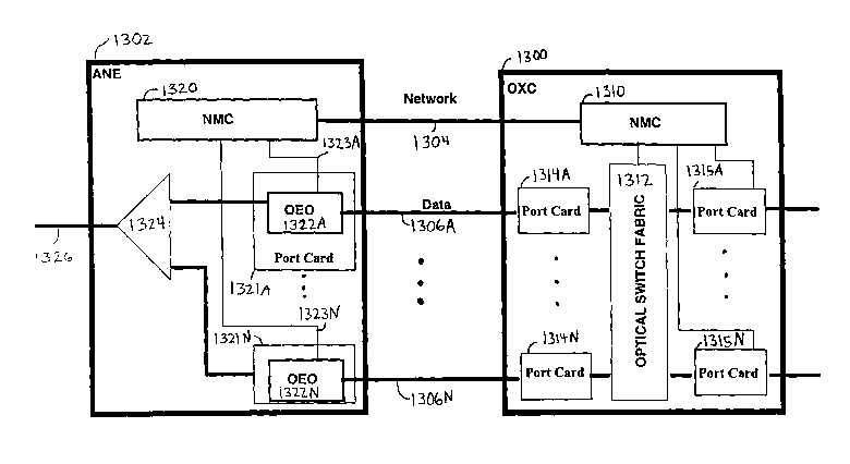
Figure 13 illustrates a block diagram of an out-of-
band signaling interface between an optical cross-connect
switch 1300 and attached network equipment 1302. The
signaling interface is realized by using an out-of-band
communication channel over a network 1304 which may also
be referred to as an out-of-band signaling channel. In-
band communication channels are those used by the optical
cross-connect switch 1300 to switch data signals on the
CA 02389758 2002-04-30
WO 01/33895 _2~_ PCT/US00/30303
one or more data signals lines 1306A-i306N. An out-of-
band communication channel is a communication channel
other than that used by the optical cross-connect switch
1300 to switch its data signals on the data lines 1306A-
1306N. The in-band communication channels used to switch
data signals on the data lines 1306A-1306N by the optical
cross-connect switch 1300 are light signals, also referred
to as photonic signals or optical signals, that are
carried in optical fibers. The data lines 1306A-1306N are
not used for the signaling interface because these lines
carry high-bandwidth signals. To convert optical signals
in the optical domain into electrical signals in the
electrical domain to extract signaling information is a
very expensive process. Indeed, a major reason for using
1~ an all-optical cross-connect is to avoid converting
signals from the optical domain to the electrical domain.
The out-of-band signaling channel is provided on a network
1304 such as a LAN, a MAN, the Internet or other 4VAN.
Each of the data lines 1360A-1306N is bi-directional to
provide duplex data communication channels. The data
lines 1306A-1306N in one embodiment include at least two
optical fibers for data flow in each direction between the
optical cross-connect switch and the attached network
equipment 1402 to provide full duplex data communication
channels. In another embodiment, each of the data lines
1306A-1306N is a single optical fiber to provide bi
directional signal flow in both directions and can be full
or half duplex data communication over a single optical
fiber. Full duplex is accomplished over a single optical
fiber by transmitting and detecting signals in the single
optical fiber at each end. The network 1304 also provides
a bi-directional out-of-band signaling channel so that
signals can be received and transmitted in each direction
between the optical cross-connect switch and the attached
CA 02389758 2002-04-30
WO 01/33895 _2g_ PCT/US00/30303
network equipment 1402 and other network equipment coupled
to the network 1304. The out-of-band signaling channel
can be either full duplex or half duplex in providing bi-
directional data communication.
Data signals from the optical cross-connect switch
1300 on the data lines 1306A-1306N are coupled into the
attached network equipment 1302. The data lines 1306A-
1306N are a light transmission media, such as optical
fibers, coupled between the optical cross-connect switch
1300 and the attached network equipment 1302 to carry or
transport the light pulses or photon pulses of the data
signals there-between. That is, the attached network
equipment 1302 is coupled or attached to the optical
cross-connect switch 1300 to accept data signals
transported over the one or more data lines 1306A-1306N.
Data signals from the attached network equipment (ANE)
1302 on the data lines 1306A-1306N are coupled into the
optical cross-connect switch 1300. The optical cross-
connect switch 1300 is coupled or attached to the attached
network equipment 1302 to accept data signals transported
over the one or more data lines 1306A-1306N.
The optical cross-connect switch 1300 includes the
network management controller (NMC) 1310 (also previously
referred to herein as a network control module (NCM)), one
or more I/0 port cards 1314A-1314N and 1315A-1315N, and
the optical switch fabric 1312. The optical switch fabric
generates optical paths therein in order to cross-connect
(also referred to as route or switch) optical signals from
an I/O port card on the input side to an I/O port card on
the output side. The optical paths are bi-directional in
that the optical signal can flow in either direction with
the optical path coupled to either an input port or an
output port of a port card. I/O port cards can also be
referred to as line cards, port cards, or I/O port modules
CA 02389758 2002-04-30
WO 01/33895 _29_ PCT/US00/30303
as previously used herein. Each of the one or more I/0
port cards 1314A-1314N and 1315A-1315N of the optical
cross-connect switch 1300 includes an optical input port
and an optical output port to couple to the optical fibers
of the full duplex data lines 1306A-1306N. Port cards
1314 can also include some simple monitoring functions by
tapping off a small percentage of the energy of the
optical signal and converting it into an electrical signal
using an inexpensive O/E. However, port cards 1314 do not
need a full-fledged receiver for extensive monitoring of
parameters such as a bit error rate or the presence of a
particular frame because the signaling interface of the
present invention is provided in order to acquire such
information from other network equipment.
The attached network equipment 1302 includes a
network management controller 1320 and one or more I/O
port cards 1321A-1321N (also referred to as line cards or
herein previously as I/O port modules). Each of the one
or more I/O port cards 1321A-1321N includes an optical-
electrical-optical converter 1322A-1322N on its data input
ports to couple to optical fibers of the data lines 1306A-
1306N. The one or more optical-electrical-optical
converters 1322A-1322N first convert the optical signals
on the data lines 1306A-1306N into electrical signals and
then convert the electrical signals into optical signals.
The one or more optical-electrical-optical converters
1322A-1322N can be used for a number of reasons including
to generate electrical signals to monitor the optical
signal as well as to amplify (i.e. regenerate) low level
incoming optical signals. In the conversion process, the
one or more optical-electrical-optical converters 1322A-
1322N provide information regarding the optical signals in
electrical form which is tapped for monitoring purposes as
the electrical signals 1323A-1323N. The electrical
CA 02389758 2002-04-30
WO 01/33895 _30_ PCT/LTS00/30303
signals 1323A-1323N may include information from other
sources of the respective port card 1315A-1315N that may
be of relevance to the optical cross-connect switch. The
one or more optical-electrical-optical converters 1322A-
1322N and their electrical signals were originally used in
the attached network equipment 1302 to facilitate its
functionality and monitor its performance and not provide
feedback to an optical cross-connect switch.
The electrical signals 1323A-1323N are coupled into
the network management controller (NMC) 1320 of the
attached network equipment 1302. In one embodiment, the
electrical signals 1323A-1323N, or a representation
thereof, are signaled back to the optical cross-connect
switch 1300 over the out-of-band signaling channel on the
network 1304. The electrical signals 1323A-1323N, or a
representation thereof, are transmitted from the network
management controller 1320 in the attached network
equipment 1302 to the network management controller 1310
in the optical cross-connect switch 1300. In this manner,
the attached network equipment 1302 signals to the optical
cross-connect switch 1300. In a similar manner with
differing information, the optical cross-connect switch
1300 can signal to the attached network equipment 1302
over the out-of-band signaling channel.
The optical-electrical-optical converters 1322A-1322N
are expensive and as a result of being already available
in the attached network equipment 1302, they are not
needed in the optical cross-connect switch 1300 if the
signaling interface of the present invention is provided.
This can provide considerable cost savings when purchasing
optical cross-connect switches 1300.
In Figure 13, the attached network equipment 1302
that is coupled to the optical cross-connect switch 1300
is a WDM line terminal 1302 which also includes a wave
CA 02389758 2002-04-30
WO 01/33895 -31- PCT/US00/30303
division multiplexer/demultiplexer 1324 along with the
network management controller 1320 and the one or more
port cards 1321A-1321N with the optical-electrical-optical
converters 1322A-1322N. The wave division
multiplexer/demultiplexer 1324 couples to a pair of
optical fibers on one end to carry wave divisioned
multiplexed signals 1326 in each direction for full duplex
communication and one or more pairs of optical fibers on
an opposite end to couple to the I/O port cards 1321A-
1321N. The wave division multiplexer/demultiplexer 1324
multiplexes multiple light signals received from
respective optical fibers in one direction into a wave
division multiplexed signal 1326 having multiple light
signals of different wavelengths carried over one optical
fiber. The wave division multiplexer/demultiplexer 1324
demultiplexes a wave division multiplexed signal 1326 in
an opposite direction having multiple light signals of
different wavelengths carried over one optical fiber into
multiple light signals for transmission to the optical
cross-connect switch 1300 over the data lines 1306A-1306N.
The wave division multiplexed signal 1326 provides greater
data bandwidth and channel capacity over an optical fiber.
The network connection to the network 1304 for the
out-of-band signaling channel is an Ethernet, an RS232 or
2~ other similar connection connecting together the network
management controllers (NMCs) (also previously referred to
as a network control module (NCM)) of the optical cross-
connect switch 1300 and the attached network equipment
1302. Because the out-of-band signaling channel is
provided over the network 1304, other network equipment or
monitoring stations can receive information and transmit
information or control signals over the out-of band
signaling channel regarding the network, the network
equipment and the optical network components connected to
CA 02389758 2002-04-30
WO 01/33895 _32_ PCT/US00/30303
the network. Thus, management of the network can be
facilitated regarding the optical cross-connect 1300, the
attached network equipment 1302, and other network
equipment using the out-of-band signaling channel. The
out-of-band signaling channel over the network can be
considered a centralized signaling interface.
Referring now to Figure 14 a block diagram of a
decentralized signaling interface between an optical
cross-connect switch 1400 and attached network equipment
1402 is illustrated. The decentralized signaling
interface is provided by one or more dedicated signal
lines 1404A-1404N between the optical cross-connect switch
1400 and the attached network equipment 1402. The one or
more dedicated signal lines 1404A-1404N can be formed by
using low-cost multimode (MM) optical fibers or by using
low cost electrical wire links.
The one or more dedicated signal lines 1404A-1404N
replaces the out-of-band signaling channel of the network
1304. Whereas the out-of-band signaling channel of the
network 1304 provided signals regarding switching each of
the optical signals on multiple communication channels,
one dedicated signal line 1404 provides information
regarding switching of optical signals on one
communication channel. Furthermore, the centralized
signaling between the between the optical cross-connect
switch 1400 and the attached network equipment 1402 was
performed by the centralized NMCs 1310 and 1320 at a
central control level. In contrast, decentralized
signaling is performed by the I/O port cards (also
referred to as line cards or herein previously as I/0
port modules) at a line-card level which is a much lower
level than the centralized NMC level.
In the embodiment illustrated in Figure 14, the
optical cross-connect switch 1400 includes the network
CA 02389758 2002-04-30
WO 01/33895 _33_ PCT/LJS00/30303
management controller (NMC) 1310, one or more I/O port
cards 1414A-1414N (also referred to as line cards, port
cards and I/0 port modules), and the optical switch fabric
1312. Each of the one or more I/O port cards 1414A-1414N
and 1415A-1415N of the optical cross-connect switch 1400
includes an optical input port and an optical output port.
Each of the one or more port cards 1414A-1414N further may
include optical-electrical converters (0/E) 1416A-1416N if
the dedicated signal line is an optical fiber. The
optical-electrical converters 1416A-1416N of the optical
cross-connect switch are much less expensive than optical-
electrical-optical converters (0/E/0) that might otherwise
be needed therein. Optical-electrical converters (0/E)
are typically a fiber optic receiver module which includes
a photodetector.
The attached network equipment 1402 includes one or
more port cards 1421A-1421N (also referred to as line
cards). Each of the one or more port cards 1321A-1321N
includes an optical-electrical-optical converter 1322A-
1322N on its data input ports to couple to optical fibers
of the data lines 1306A-1306N. In the case the dedicated
signal lines 1404A-1404N are optical fibers, each of the
one or more port cards 1321A-1321N further includes an
electrical-optical converter (E/0) 1422A-1422N to convert
electrical signals 1423A-1423N into optical signals.
Electrical-optical converters (E/0) are typically a fiber
optic transmitter module which include a semiconductor
laser with control electronics. Optical-electrical-
optical converters (0/E/0) are typically a combination of
an 0/E converter coupled together with an E/0 converter.
The attached network equipment 1402 that is
illustrated coupled to the optical cross-connect switch
1400 is a WDM line terminal 1402. A WDM line terminal
1402 also includes a wave division multiplexer 1324 along
CA 02389758 2002-04-30
WO 01/33895 -34- PCT/LTS00/30303
with the one or more port cards 1421A-1421N with the
optical-electrical-optical converters 1322A-1322N.
The one or more optical-electrical-optical converters
1322A-1322N first convert the optical signals on the data
lines 1306A-1306N into electrical signals and then convert
the electrical signals into optical signals. The one or
more optical-electrical-optical converters 1322A-1322N are
tapped to provide information regarding the optical
signals in electrical form on the electrical signals
1323A-1323N. The port cards 1421A-1421N of the attached
network equipment 1402 detect other relevant information
and communicate it directly to the respective port cards
1414A-1414N of the optical cross-connect switch 1400 over
the dedicated signal lines 1404A-1404N rather than
signaling between the central NMCs 1310 and 1320.
Similarly, port cards 1414A-1414N of the optical cross-
connect switch 1400 can detect relevant information and
communicate it directly to the respective port cards
1421A-1421N of the attached network equipment 1402 over
the dedicated signal lines 1404A-1404N.
Having established a signaling interface, it can be
used for several purposes. The signaling interface can be
used to enable fast network restoration through the
optical cross-connect switch (OXC) in the event of network
failures. Network failures include signal failures such
as a loss of signal (LOS) or signal degradation such as
through a bit error rate (BER) or other commonly know
optical failure mechanisms. Attached network equipment
(ANE) can detect failures in real time by using its O/E/Os
and convey this information to the optical cross-connect
switch over the signaling interface so that it can perform
network restoration. The optical cross-connect switch is
typically without O/E/Os and may not be able to detect the
CA 02389758 2002-04-30
WO 01/33895 _35_ PCT/US00/30303
failure due to the otherwise relatively simple monitoring
usually found within an optical cross-connect switch.
Another use for the signaling interface is to allow
attached network equipment (ANE) to control the optical
cross-connect switch (OXC). For example, the attached
network equipment (ANE) could signal to the OXC over the
signaling interface in order for it to provide a
particular switch configuration.
Another use for the signaling interface is so that
the optical cross-connect switch can signal to the
attached network equipment to set specific parameters
therein. For example during setting up a connection, the
optical cross-connect switch may ask the attached
equipment to adjust its transmitter power level.
Another use for the signaling interface is to allow
attached network equipment (ANE) to request a connection
through the optical cross-connect switch (OXC). The
optical cross-connect switch (OXC) sets up the connection
and informs the attached network equipment (ANE) when its
available.
Another use for the signaling interface is to perform
protection switching between the OXC and the attached
network equipment. For example, the signaling interface
could be provided by one spare fiber facility for N
working facilities between the attached equipment and the
OXC. If one of these N facilities fails, the signaling
channel is used by both devices to switch connections from
the failed facility to the spare facility.
The present invention is thus described and has many
advantages over the prior art. One advantage of the
present invention is that the costs of optical cross-
connect switches can be reduced by utilizing the signaling
interfaces of the present invention. Another advantage of
the present invention is that real time performance
CA 02389758 2002-04-30
WO 01/33895 _36_ PCT/C1S00/30303
information can be obtained. Still another advantage of
the present invention is that control and monitoring of
the performance of an optical cross-connect switch can be
performed over the network of the out-of-band signaling
interface.
While certain exemplary embodiments have been
described and shown in the accompanying drawings, it is to
be understood that such embodiments are merely
illustrative of and not restrictive on the broad
invention, and that this invention not be limited to the
specific constructions and arrangements shown and
described, since various other modifications may occur to
those ordinarily skilled in the art. Additionally, it is
possible to implement the present invention or some of its
features in hardware, firmware, software or a combination
thereof where the software is provided in a processor
readable storage medium such as a magnetic, optical, or
semiconductor storage medium.