Note: Descriptions are shown in the official language in which they were submitted.
PCT/NZ00/00127
Received 12 September 2001
METHOD AND APPARATUS FOR TESTING A SENSOR
Field of the Invention
The present invention relates to a method and apparatus for testing a
sensor, such as a capacitive sensor.
Background of the Invention
In certain applications which employ a capacitive sensor, such as bio-
medical applications, the output of the sensor is critical to the
operation of a device. Therefore a need exists for an efficient method
of testing the operation of the sensor, and at least providing an
indication if abnormal operation is detected.
JP-A-06318744 describes a sensor comprising a piezoelectric material
affixed on both surfaces with a pair of electrodes. Each electrode is
formed in a U-shape with a pair terminals, one at each end.
Discontinuities in each electrode can be detected by measuring the
resistance between a respective pair of terminals.
A problem with the arrangement of JP-A-06318744 is that the
electrodes must be formed into a special shape. Another problem is
that it is not possible to detect discontinuities between the electrodes,
for instance due to a b~~eakdown in the piezoelectric material.
An object of the invention is to address these problems, or at least to
provide the public with a useful alternative.
Summary of the Invention
In accordance with a first aspect of the present invention there is
provided apparatus for testing a sensor having a sensor output line,
the apparatus including:
4MENGED SHEET
CA 02390176 2002-05-02
tPFJJ~/AU
f
Y(:'1'INGUU/UU 127
CA 02390176 2002-05-02 Received 12 September 2001
2
means for applying a test input signal to the sensor output line,
the test input signal having a predetermined signal characteristic; and
means for monitoring a sensor output signal from the sensor on
the sensor output line and generating a test output signal which varies
in accordance with the presence or absence of the predetermined
signal characteristic in the monitored sensor output signal.
In accordance with a second aspect of the invention there is provided
a method of testing a sensor having a sensor output line, the method
1o including the steps of:
applying a test input signal to the sensor output line, the test
input signal having a predetermined signal characteristic; and
monitoring a sensor output signal from the sensor on the sensor
output line and generating a test output signal which varies in
accordance with the presence or absence of the predetermined signal
characteristic in the r,~onitored sensor output signal.
The test input signal can be applied across the sensor without creating
unwanted interference with sensing signals which are generated by the
sensor during normal operation land which will not, in general, possess
the predetermined signal characteristic).
In one embodiment the test signal lies within a test frequency range,
and the means for monitoring blocks signals outside the test frequency
range (typically employing a band-limiting filter such as a high-pass,
low-pass, comb, notch or band-pass filter). Typically the test signal is
substantially sinusoidal.
Typically the apparatus further includes means for extracting a sensing
signal from the sensor outout signal by blocking signals outside a
sensing frequency range (typically a band-limiting filter such as a high-
pass, low-pass, comb, notch or band-pass filter).
4MENDED SHEET
m~Au
PCT/NZ00/00127
CA 02390176 2002-05-02 Received 12 September 2001
3
Typically there is no overlap between the two frequency ranges. In
other words the test frequency range lies completely above or
completely below the sensing frequency range.
In an alternative embodiment the test input signal is encoded with a
predetermined code sequence (such as a psuedo-random sequence),
and the test output signal is generated by correlating the
predetermined code sequence with the sensor output signal.
to Typically the test input signal is applied to the sensor via an impedance
element leg. a capacitor, resistor, inductor or combination thereof).
Preferably the impedance element has an impedance at least 10-100
times greater than the impedance of the sensor, at the frequency of
the test signal.
At its most basic level the apparatus may simply be used to check the
presence or absence of the sensor. During normal operation, the
sensor will present a known impedance to the test input signal.
However if a fault exists the sensor will present a higher or lower
2o impedance to the test signal. This can be detected and used to
generate a two-level test output signal lie. a signal with one level
j'during normal operation and another level when the impedance
measurement lies outside predetermined performance criteria). In a
preferred embodiment a fault signal is generated when the impedance
of the sensor lies outside predetermined performance criteria.
In an alternative, more complex system, the test output signal has
more than two output values, if for example the sensor is a capacitive
sensor which can significantly vary its capacitance value as a part of
3o its normal operation.
Typically the apparatus is used to monitor a movement sensor
comprising a piezoelectric material which generates sensing signals by
movement of the piezoelectric material.
'.MELDED SHEET
IPE.A/AU
CA 02390176 2002-05-02
WO 01/33245 PCT/NZ00/00217
4
The invention may be employed in a variety of applications. For
instance the sensor may acquire signals from a human or animal
subject. One example of such a biomedical system is an infant apnoea
monitoring system which employs a capacitive piezoelectric sensor to
acquire cardiac, respiratory and/or large motor movement data from an
infant during sleep. Another example is an automobile driver
monitoring system in which a capacitive piezoelectric sensor mounted
in an automobile seat acquires cardiac, respiratory and/or large motor
movement signals from a driver of the automobile.
Brief Description of the Drawings
A number of examples of the present invention will now be described
with reference to the accompanying drawings, in which:
Figure 1 is a schematic circuit diagram of a single-ended piezoelectric
sensor system incorporating a sensor testing circuit with the test
frequency above the sensor system frequency bands of interest;
Figure 2 is a schematic circuit diagram of a differential piezoelectric
sensor system incorporating a first sensor testing circuit with the test
frequency above the sensor system frequency bands of interest;
Figure 3 is a schematic circuit diagram of a differential piezoelectric
sensor system incorporating a second sensor testing circuit;
Figure 4 is a schematic circuit diagram of a differential piezoelectric
sensor system incorporating a third sensor testing circuit;
Figure 5 is a schematic circuit diagram of a piezoelectric sensor system
incorporating a fourth sensor testing circuit which includes a pseudo-
random noise generator; and
CA 02390176 2002-05-02
WO 01/33245 PCT/NZ00/00217
5
Figure 6 is a schematic circuit diagram of a linear feedback shift
register.
Detailed Description of the Preferred Embodiments
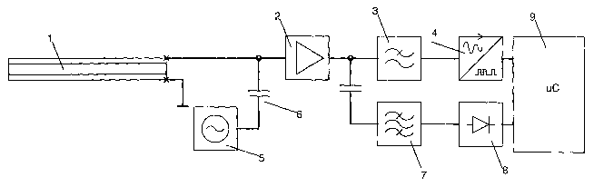
Referring to figure 1, a piezoelectric sensor 1 comprises a sheet of
polyvinylidene fluoride (PVDF) film with a pair of electrodes arranged
on opposite sides of the film. One electrode is connected to ground
and the other electrode is connected to a sensor output line. The
PVDF film can be made in quite large sizes. For the purposes of this
example, we can assume that a standard A4 sheet size would have a
capacitance of somewhere between 10 nF and 40 nF, depending on
the thickness of the film. Deformation of the film results in the
generation of a sensing signal on the sensor output line. The relatively
high capacitance of the film means that the sensing signal lies in a
relatively low frequency band, below 35 Hz for instance. The sensor
output signal on the sensor output line is amplified by an amplifier 2,
filtered by a lowpass filter 3 which rolls off at 35 Hz, passed on to
electronics 4 (eg. analog-to-digital converter etc), and processed by a
microprocessor 9.
An oscillator 5 generates an oscillating test input signal at a frequency
of 10 KHz. The test input signal is applied to the sensor output line
via a small capacitor 6 (or a high-valued resistor or resistor/inductor
combination) with an impedance 10-100 times greater than the
impedance of the sensor 1 (at the test frequency) so as not to load the
sensor 1 . During normal operation, the relatively low impedance
sensor 1 effectively short-circuits the 10KHz signal to ground.
A bandpass filter 7 is coupled to the output of the amplifier 2 via a
capacitor (not labelled). The filter 7 has a bandpass region centred on
the 10KHz test signal frequency. Thus any signals at the 10KHz test
frequency are passed onto a diode 8 and the microprocessor 9, and
any signals in the 0-10Hz sensing signal frequency band are blocked.
CA 02390176 2002-05-02
WO 01/33245 PCT/NZ00/00217
6
During normal operation, with the test input signal effectively short-
circuited by the sensor 1, the test signal voltage output by the
bandpass filter 7 will lie below a predetermined threshold. However, if
a fault is present and the 10KHz test signal is not short circuited by
the capacitive sensor, then the test signal voltage level will rise above
the threshold. In this case the microprocessor 9 generates a fault
detection signal. The microprocessor can simultaneously monitor the
detected test signal from diode 8 and process the sensing signal from
electronics 4.
In the example of Figure 2, a sensor 10 comprises a film sheet and
electrodes (not labelled) encased in a grounded electrostatic shield 1 1 .
Differential outputs 12,13 of the sensor 10 are coupled to positive and
negative input terminals of a differential amplifier 16. The output of
the differential amplifier 16 is input to electronic circuitry (not shown)
similar to items 3,4,7,8 and 9 shown in Figure 1 .
A high frequency oscillator 15 is coupled to one output 12 of the
sensor 10 via a capacitor (not labeled) with an impedance at least 10-
100 times greater than the impedance of the sensor 1 (at the test
frequency). A high frequency decoupling capacitor 14 (with a
relatively high impedance at the sensor measurement frequency band,
but with a relatively low impedance at the test frequency) is connected
between the other differential output 13 and ground to complete the
shunt to ground.
As in the Figure 1 circuit, during normal sensor operation little test
signal is present on the output of the differential amplifier 16.
Figure 3 shows the differential sensing circuit of Figure 2 but with a
different sensor testing circuit. In this case the ground shunt capacitor
14 is omitted. The test input signal is applied to one differential
output of the sensor and a test signal detection circuit 18 (comprising
CA 02390176 2002-05-02
WO 01/33245 PCT/NZ00100217
7
a capacitor, bandpass filter and diode) is coupled to the other
differential output of the sensor.
In the Figure 3 example, in contrast to the Figure 1 and 2 examples,
during normal operation the test signal will be passed onto the
detection circuit 18. Thus the test signal detection circuit 18 outputs a
signal to the microprocessor (not shown) which generates a fault
detection signal when the test signal output by the bandpass filter falls
below a predetermined threshold.
Figure 4 shows the differential sensing circuit of Figures 2 and 3 but
with a third different sensor testing circuit. In this case the test input
signal is applied by a differential oscillator drive 19 via a pair of
capacitors (not labelled) each with an impedance at least 10-100 times
1 s greater than the sensor 1 . As in the Figure 2 example, during normal
operation little test signal is present on the output of the differential
amplifier.
The testing circuits of Figures 1-4 all simply illustrate an out-of-band
single-frequency detection circuit much higher in frequency than the
sensor's target frequency range. It will be appreciated that the same
principles apply to a sensor configuration where the test frequency is
below the frequency bands of interest from the sensor. Under these
circumstances, the sensor frequency bands are isolated instead with
highpass filtering.
The testing circuits of Figures 1-4 all simply provide a two-level go/no-
go output. However it will be appreciated that the test input signal
may also be used to provide a more accurate measurement of the
impedance of the capacitive sensor, and hence the sensor integrity.
Thus in an alternative example (not shown), the microprocessor 9
monitors the test signal level from the bandpass filter by means of an
analogue to digital converter and provides the measurement for
display, recording, or other indication.
e blocked.
3
CA 02390176 2002-05-02
WO 01/33245 PCT/NZ00/00217
8
The accurate impedance measurement can be used to determine
whether the sensor 1 has been partially damaged, for instance by
being cut. Alternatively the multi-level output may be useful in
applications in which the capacitance of the sensor is varied as part of
the normal operation of the sensor.
A further extension of the same principle can utilize instead of single-
frequency signals for monitoring of the impedance of the sensor, a
band of such frequencies. A pseudo-random sequence is one example
that lends itself to simple generation and detection. Furthermore, a
pseudo-random sequence can be used not only above or below the
sensor frequency bands, but may also be used directly in the sensor's
frequency range of interest, as is applied in spread spectrum
I > techniques. Given that the applied Pesudo Random Sequence test
signal is known, it may be detected by means of correlation, and
thereby separated from the sensor measurement signal. The detected
level is then processed as in the previous examples.
An example of a system embodying this principle is shown in Figures 5
and 6. Figure 5 is identical to Figure 1 except the oscillator 5 has
been replaced with a pseudo-random noise generator 25, the band-
pass filter 7 has been replaced by a correlator 26 and the diode 8 has
been replaced by an averager 27.
The generator 25 may be implemented in the form of a linear feedback
shift register shown in Figure 6 (although many different forms of
implementation are known in the literature). A clock signal 20 is
supplied to a chain of series-connected flipflops 23. Selected taps of
3o the shift register are summed together with exclusive-OR gates 24 in
order to provide a maximal-length sequence of 2"N - 1, where N is the
number of flipflops 23 in the shift register. The actual tap points for a
maximal length sequence vary with the length of the shift register, but
CA 02390176 2002-05-02
WO 01/33245 PCT/NZ00/00217
9
are well known and published in the literature or are relatively easily
determined.
An output 21 of the generator 25 is fed back to the input 22. As a
result, the signal on output 21 is a pseudo-random binary sequence
(PRBS) which is uniquely determined by the configuration of tap points
for the exclusive-OR gates 24.
The pseudo-random binary sequence is also fed to a correlator 26
l0 which generates an output with a DC level (measured by averager 27)
which is indicative of the degree of correlation between the output of
the sensor and the PRBS. The correlation function implemented by the
correlator 26 might, for instance, be carried out by way of a simple
phase sensitive detector and low pass filter to both block the sensing
15 signal and recover the test signal.
In applications where the sensor measurement signal is of narrow
bandwidth, the broad spectral nature of the PRBS may mean that the
PRBS may be sufficiently removed from the sensing signal by the
20 LPF 3. Alternatively the PRBS may be completely removed from the
sensing signal by correlation and subtraction utilising digital signal
processing techniques.
Although this invention has been described by way of example it is to
25 be appreciated that improvement and/or modifications may be made
thereto without departing from the scope of the invention as defined in
the appended claims.