Note: Descriptions are shown in the official language in which they were submitted.
CA 02390498 2002-05-08
-1-
METHOD AND DEVICE FOR PRODUCING A SOLDERED JOINT
The present invention relates to a method for thermal treatment of
workpieces or components, in particular for producing a soldered joint
between a solder material and at least one component or workpiece used
as a solder material carrier by melting of the solder material arranged on
the solder material carrier, wherein at least one component is heated in a
process atmosphere sealed off from the environment. In addition, the
invention relates to a device appropriate for carrying out this method.
A method or a device of the aforementioned type is known from DE
29 08 829 C3 which describes a method for performing a hard soldering
procedure in an evacuated process chamber, wherein components to be
joined together by melting of a hard solder are joined together. During
the hard solder procedure a vacuum is formed in the process chamber and
heating of the components to be joined together takes place at
approximately 600 C.
With this known method a subsequent cooling procedure takes place
outside the process chamber in a normal environmental atmosphere.
US 5,782,402 describes a method and a device for producing a soldered
joint, whereby the device comprises three chambers which are evacuated
for performing the method, such that both the heating and cooling
procedure take place in a vacuum. Simultaneous loading of the chambers
and thus increased conversion are enabled by the chambers sealed off
from the environment.
CA 02390498 2008-07-03
-la-
US 5,341,978 describes a device for carrying out a soldering procedure
which takes place in a nitrogen atmosphere to avoid oxidation of the
workpieces, whereby the nitrogen introduced into the chambers is first
evaporated in a cavity limited by an inner and an outer wall of the
cooling chamber in order to then be conveyed from the cavity limited by
the chamber walls to the inside of the chambers. There it serves as
cooling or oxidation protection. The heat released by the cooling method
is used at the same time to accelerate heating of the gas.
The object of the present invention is to propose a method or a device,
wherein not only heating of a component, in particular for melting the
solder material, but also cooling of the component in a defined process
atmosphere take place, without the heating procedure and the cooling
procedure impairing each other.
A process for producing a soldered joint between a solder material and at
least one
component serving as a carrier for said solder material, by melting of the
solder material
arranged on the carrier, wherein heating of the at least one component and
cooling of the at
least one component in a subsequent procedural step take place in a process
atmosphere
which is sealed off from the environment, whereby the heating and cooling of
the at least
one component take place in process chambers independent of one another with
process
atmospheres differing from one another, and controlling of temperature for
heating the at
least one component or for cooling the at least one component occurs by way of
a tempering
device which is heated or cooled, such that the tempering device for heating
or cooling is
operated at a substantially constant temperature, whereby the tempering device
is operated
as a radiator device, characterised in that the radiator device is combined
with a contact
device, such that temperature controlling takes place at least in one starting
phase of the
heating or cooling by means of conveying heat or cold and a temperature
setting of the at
least one component is adjusted by the distance of the radiator device from
the at least one
component.
In the process according to the present invention cooling of the
CA 02390498 2002-05-08
-2-
component takes place in a procedural step following on from the
heating step in a process atmosphere sealed off from the environment,
whereby heating of the component or melting of the solder material and
cooling of the component takes place in process chambers independent of
one another.
The method according to the present invention basically lends itself for
use generally for temperature application to workpieces or components
for thermal treatment, such as tempering, annealing and the like, for
example. A particular area of application is the production of soldered
joints which can be designed both as hard soldered joint and as soft
soldered joint, such as for example in the manufacture of electronic
components and assemblies.
With the manufacture of soldered joints in particular the method
according to the present invention enables not only a cooling procedure
controlled similarly to the melting procedure without the procedures
mutually influencing one another, but also effective execution of the
soldering procedure including the cooling procedure based on the
process chambers specified with respect to their task in each case.
Reciprocal influencing of both procedures is opposed by the possibility
of the formation of different process atmospheres in the various process
chambers. In addition, an overall higher quality of the soldered joint
results from the cooling carried out in a defined process atmosphere.
This proves to be particularly advantageous whenever the soldered joint
has not only mechanical connecting functions, as with the connection
between metallic components, but also an electrical connecting function,
such as for example in the case of boards fitted with electronic
components in the SMD (surface-mounted device) method and which are
connected by way of a soldered joint mechanically and electrically
conductively to the strip conductors of the boards.
!i
CA 02390498 2002-05-08
-3-
With use of the method according to the present invention for
mechanically connecting metallic components by means of a soldered
joint in particular it proves to be advantageous if in a procedural step
preceding melting of the solder material the solder material carrier is
prepared by application with a reducing or inert process atmosphere
and/or by radiation or with materials in a separate process chamber. This
makes it possible, without impairing a process atmosphere particularly
suitable for the subsequent melting procedure, to prepare the solder
material carrier, for example the metallic components. For this purpose it
may be possible to introduce a reduction agent, such as formic acid or
the like, into the process chamber, or also to generate a reducing gas
atmosphere in the process chamber, whereby before the solder material
carrier or the components to be joined together are transferred to the
subsequent process chamber for performing the melting procedure the
process chamber can be rinsed to counteract any influence of the process
atmosphere which has formed in the subsequent process chamber. Such
preparation of the solder material carriers or of the components to be
joined together can also be effected by plasma application of the
components or of the contact surfaces to be moistened with the solder
material in the subsequent melting procedure.
A further possibility of counteracting reciprocal influence of the various
process atmospheres which have formed in the various process chambers,
consists of establishing a vacuum in the respective process atmospheres
or the process chambers.
There is also the possibility of creating the process atmosphere in each
process chamber as a protective gas atmosphere.
The simplest possible method for adjusting the temperature of the
component is feasible if the temperature application occurs by means of
a tempering device which is operated to heat or cool the component with
^
CA 02390498 2002-05-08
-4-
a substantially constant temperature. This altogether enables short
processing times, because heating or cooling times of the tempering
device do not apply with continuous operation of the tempering device.
For shortening the tempering period or for increasing the tempering rate
it has proven advantageous if the temperature of the tempering device is
selected clearly higher than the desired processing or soldering
temperature.
The simplest possible method for adjusting the temperature of the solder
material and/or of the solder material carrier when a soldered joint is
being produced is likewise enabled by such a temperature application.
An advantageous form of regulating is enabled if the tempering device is
operated as a radiator device, and the temperature of the component or of
the solder material carrier is adjusted over the distance of the radiator
device from the component or from the solder material carrier.
If the radiator device is combined with a contact device and temperature
application occurs at least in one starting phase of the heating or cooling
by means of conveying heat or cold, then it is possible to considerably
shorten the heating or cooling periods.
The device according to the present invention for carrying out the
abovementioned method has a heating chamber or a melt chamber, in
which heating of the component takes place, in particular for melting a
solder material for producing a soldered joint arranged on a component
serving as solder material carrier, and a cooling chamber for cooling the
component attached to the melt chamber, whereby the heating chamber
or the melt chamber and the cooling chamber form process chambers
independent of one another.
For preparing the solder material carrier for the soldered joint a
CA 02390498 2002-05-08
-5-
preparation chamber, which forms a process chamber independent of the
melt chamber, can be arranged in front of the melt chamber.
If the process chambers are designed as separate modular units, which
can be connected to one another via door mechanisms, the device
according to the present invention can easily be adapted in construction
to various methods, so that for example in one particular case the device
can be constructed only from a melt chamber and a cooling chamber as
required, and in another case by a preparation chamber, a melt chamber
and a cooling chamber, whereby at least partially identical modular units
can be utilised to construct the respective device.
It is also possible to build up the process chambers in a modular fashion,
in such a way that the door mechanisms are designed as door modules
and can be combined with chamber modules to construct the process
chambers.
For temperature application of the component arranged on a carrier
device in the process chambers formed by the melt chamber or the
cooling chamber it is an advantage to provide a radiator device which
can be altered in its distance relative to the carrier device or the
component by means of a distance alteration device. A temperature
application device so designed enables the radiator device to be operated
at an essentially constant temperature, whereby the distance of the
radiator device relative to the carrier device can be altered to make a
change to the temperature of the carrier device heated by the radiator
device.
In the need to accelerate heating of the carrier device and thus overall to
shorten the sojourn time of the solder material carriers necessary for
carrying out the melting in the melt chamber or the instances of cooling
in the cooling chamber, it has also proven advantageous to provide the
CA 02390498 2002-05-08.
-6-
radiator device with a contact device which also enables temperature
transmission via heat conduction, apart from temperature transmission
via radiation. With use of the radiator device for cooling the component
or the solder material carrier the radiator device can be combined with a
convection device to improve cooling efficiency.
The simplest possible design of the radiator device with simultaneous
formation of a contact device is feasible if the radiator device is
designed as a temperable plate, whose surface serves as contact device.
To regulate the distance of the radiator device from the carrier device
depending on a desired temperature of the carrier device it proves
advantageous to provide the carrier device or the solder material carrier
with a temperature sensor, whose output signal serves to define a
correcting variable for altering the distance of the radiator device
relative to the carrier device. The temperature sensor, which serves to
determine the temperature of the carrier device, can also be arranged
directly on the radiator device, thus for example on the plate, whereby a
touch contact with the carrier device can be guaranteed by a connecting
device compensating the modified distance between the plate and the
carrier device, such as for example a spring device, independently of the
respective distance between the plate and the carrier.
In particular, when the method according to the present invention is
designed as a continuous process, wherein the solder material carriers
arranged on the carrier device are guided through the subsequently
arranged process chambers in a clocked manner while specific sojourn
times in the individual process chambers are adhered to, it has proven
advantageous to fit the carrier devices with an information medium
which cooperates with a reader device, such that after a carrier device
enters a first process chamber the process running in the first and
subsequently arranged process chambers is controlled by the information
^'
CA 02390498 2002-05-08
-7-
contained on the information medium.
A particularly economical application of the device is feasible if the
device comprising at least one heating chamber and a cooling chamber is
integrated into a working or manufacturing line as part device in an in-
line arrangement. When the device for producing SMD boards is used a
mounting device for mounting the SMD boards can be connected to the
device, for example.
A preferred variant of the method according to the present invention as
well as an exemplary device are explained in greater detail hereinbelow
with reference to the diagrams, in which:
Fig. 1 is a simplified perspective illustration of a possible
embodiment of the device according to the present
invention;
Fig. 2 is a longitudinal sectional illustration of the device shown in
Fig. 1;
Fig. 3 shows a door mechanism;
Fig. 4a is an illustration of an embodiment of the radiator device in
a basic configuration;
Fig. 4b shows the radiator device illustrated in Fig. 3a in a heating
configuration;
Fig. 4c shows the radiator device illustrated in Fig. 3a in a
temperature control configuration.
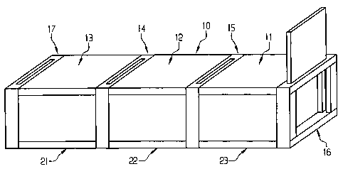
Fig. 1 illustrates a soldering device 10 with several process chambers
CA 02390498 2002-05-08
-8-
arranged in series, namely a preparation chamber 11, a melt chamber 12
and a cooling chamber 13. The separate process chambers 11, 12 and 13
are connected to one another by way of door mechanisms 14 and 15,
whereby in addition to this in the illustrated embodiment the outer
process chambers 11 and 13 each have a door mechanism 16 or 17 for
entry or exit of the carrier devices 18 illustrated in Fig. 2. Solder
material carriers are arranged on the carrier devices 18 (not illustrated
here in greater detail) which are to be provided with soldering or a
soldered joint by melting a solder material.
As clearly shown in Fig. 1, the individual process chambers 11, 12 and
13 are designed in a modular fashion and each exhibits a chamber
module 21 complemented by at least one door mechanism 14, 15, 16 or
17 which is combined with the chamber module 21, 22 or 23 to form the
respective process chamber. It is apparent from this that the series
arrangement of a total of three process chambers for forming the
soldering device 10 illustrated in Fig. 1 can be complemented by
connecting other process chambers in a modular fashion, to be able to
connect other uncoupled partial processes for expanding the process,
apart from the partial processes of the overall process uncoupled from
one another and running in the preparation chamber 11, the melt chamber
12 and the cooling chamber 13.
As illustrated by Fig. 2, the soldering device 10 illustrated here by way
of example enables a method to be carried into effect, wherein in a first
procedural step the solder material carrier or carriers, not shown here in
greater detail, are first prepared in the preparation chamber 11. For this
the carrier device 18 is introduced into the preparation chamber 11,
followed by evacuation of the preparation chamber 11 and/or addition of
a reducing agent to the preparation chamber 11 to create the desired
process atmosphere. In the event where the solder material carriers, not
illustrated in greater detail here, are metallic components to be joined to
CA 02390498 2002-05-08
-9-
one another by means of a soldered joint, it may be conceivable to create
a reducing process atmosphere by addition of formic acid in the
preparation chamber 11. After the desired reduction result is achieved
the preparation chamber 11 can be rinsed with a nitrogen/hydrogen gas
mixture.
The carrier device 18, as illustrated in Fig. 2, is arranged in the
preparation chamber 11 on a transport device 27 which enables the
carrier device 18 to be retracted into the preparation chamber 11 via the
open door mechanism 16, as well as enabling transfer of the carrier
device 18 to the melt chamber 12 after the door mechanism 15 is opened.
After the desired process atmosphere has been set in the melt chamber
12, for example after creating a reducing atmosphere, or also an inert
atmosphere by formation of a protective gas atmosphere in the melt
chamber 12, heating of the carrier device 18 to the desired soldering
temperature is carried out. Such heating is carried out by means of a
heating device 24 which has a hot plate 26 arranged on a hoisting
mechanism 25.
Fig. 3 shows an example of the structure of a door mechanism 14, 15 or
16. The door mechanism 14 enables - as indicated by the double arrow in
Fig. 3 - sealing of the process chambers 11, 12, 13 independent of the
direction of pressure to create the varying process atmosphere formed in
the process chambers 11, 12, 13 (Fig. 2). The door mechanism 14 has an
actuation device 39 here formed by a double actuating cylinder, a guide
device 40 and a door panel 41, which by means of the guide device 40
can be moved away towards a door opening 42 of a process chamber wall
43, or from the door opening 42. In the illustration according to Fig. 3
the door panel 41 is positioned directly in front of the sealing
arrangement on the process chamber wall 43. The guide device 40
comprises a slide rod 44 arranged parallel to the plane of the door
opening 42 along which a double knee lever 45 is guided by means of a
CA 02390498 2002-05-08
-10-
slide block 46. To transfer the door panels 41 from an opening position
into a closed position the slide block 46 is moved downwards starting
from an upper slide stop 47, until the travel movement of an actuating
cylinder piston 49 acts directly on the double knee lever 45 after a lower
slide stop 48 is reached, such that the door panel 41 is moved towards
the process chamber wall 43 until a seal is obtained.
A possible construction of the heating device 24 and its functioning is
explained in greater detail with reference to Figs. 4a to 4c. Fig. 4a shows
the heating device 24 in its basic configuration, in which the hot plate 26
is located at a distance dl from the carrier device 18 underneath the
carrier device 18. As Fig. 4a further depicts, the carrier device 18 is held
in its relative position compared to the heating device 24 by the
transport device 27 which in the present case is formed by feed billets 28
and 29 rotating in the vicinity of the process chambers 11, 12 and 13.
In the present case the hot plate 26 is arranged on a hoist mechanism 25
formed by two lifting rams 30 and has a temperature sensor 32 housed in
a spring arrangement 31. In the basic configuration illustrated in Fig. 4a
the spring arrangement 31 is unstressed, so that the temperature sensor
32 is arranged projecting out of a contact surface 33 of the hot plate 26.
Fig. 4b now shows the heating device 24 in its heating configuration, in
which the hot plate 26 lies with its contact surface 33 on an underside 34
of the carrier device 18, effectively transferring heat from the hot plate
26 to the carrier device 18 by thermal diffusion. At the same time the
temperature sensor 32 is located in its position sunk in the contact
surface 33 with its sensor surface 35 arranged flush in the contact
surface 33, thus lying with the sensor surface 35 likewise on the
underside 34 of the carrier device 18. The hot plate 26 is operated at a
constant temperature and remains in the contact position illustrated in
Fig. 4b until the temperature sensor 32 determines the desired
CA 02390498 2002-05-08
-11-
temperature of the carrier device 18. Next, the hot plate 26 moves to a
temperature control configuration illustrated in Fig. 4c, where the
contact surface 33 of the hot plate 26 stands at a distance d2 from the
underside 34 of the carrier device 18, whereby the temperature sensor 32
coerced by the spring arrangement 31 remains with its sensor surface 35
in contact with the carrier device 18. In the illustrated temperature
control configuration of the hot plate 26 the hot plate 26 acts only as a
radiator device and enables heat absorption in the carrier device 18 via
radiation. This effectively prevents the temperature of the carrier from
rising above the desired temperature by continuous application of the hot
plate 26 operating at a constant temperature on the carrier device 18.
Hereinbelow a change in the distance d2 between the underside 34 of the
carrier device 18 and the contact surface 33 of the hot plate 26 is set
depending on the temperature differences determined by the temperature
sensor 32 relative to the nominal temperature of the carrier device by
means of a setting device, not shown here in greater detail, as often as
necessary, such that the nominal temperature of the carrier device 18 is
kept above the sojourn time of the carrier device 18 required to realise
the melting procedure in the melt chamber 12.
The abovedescribed distance control can occur, as indicated by the
dashed representation in Fig. 4a, by means of a distance alteration device
which provides a hoisting device 50 acting on the transport device 27 or
the feed billets 28, 29 instead of a hoisting device 25 acting on the hot
plate. Essential for temperature control with a hot plate 26 operated
essentially at a constant temperature is the possibility of altering the
relative distance between the hot plate 26 and the carrier device 18 or
the solder material carrier.
As illustrated in Figs. 4a to 4c, the effect of the heating device 24 can be
further complemented as required by additional heating devices, as for
example a radiant panel heating 36 arranged here above the carrier
CA 02390498 2008-07-03
-12-
device 18. The radiant panel heating 36 can also be provided with a
distance control corresponding in its working method to the distance
control of the heating device 24.
As illustrated in Fig. 2, on completion of the melting phase in the melt
chamber 12 the carrier device 18 is transferred to the cooling chamber
13, where a process atmosphere corresponding to or differing from the
process atmosphere in the melt chamber 12 can be built up. The cooling
chamber 13 is provided with a cooling device 37 which corresponds in
particular with respect to the distance control in its design and working
method to the heating device 24 illustrated in detail in Figs. 4a to 4c.
The cooling device 37 enables defined cooling of the carrier device 18
by a combination of cold radiation and cold diffusion, for example by
effecting a predetermined cooling curve. Similarly to the heating device
24 the cooling device 37 can also be operated at a constant temperature,
whereby the temperature of the carrier device 18 can be influenced by a
change or adjustment of the distance between a cool plate and the
carrier device 18.