Note: Descriptions are shown in the official language in which they were submitted.
i-- ;~' l-~:1 UI II w,
CA 02390677 2002-06-14
16017445
1
ELECTRONIC DEVICE HAVING A GETTER USED AS A CIRCUIT ELEMENT
BACKGROUND OF THE INVENTION
The ability to maintain a low pressure or vacuum for a prolonged period in
a microelectronic package is increasingly being sought in such diverse areas
as
field emission displays (FEDs), micro-electro-mechanical systems (MEMS) and
atomic resolution storage devices (ARS). For example, computers, displays, and
personal digital assistants may all incorporate such devices. Both FEDs and
ARS typically require two surfaces juxtaposed to one another across a narrow
vacuum gap. Typically, electrons must transverse this gap either to excite a
phosphor in the case of FEDs or to modify a media to create bits in the case
of
ARS.
One of the major problems With vacuum packaging of electronic devices is
the continuous outgassing of hydrogen, water vapor, carbon monoxide, and
other components found in ambient air, and from the internal components of the
electronic device. To minimize the effects of outgassing one typically uses
gas-
absorbing materials commonly referred to as Better materials. Normally a
separate cartridge, ribbon or pill incorporates the Better material that is
inserted
into the electronic vacuum package. Thus, in order to maintain the low
pressure,
over the lifetime of the electronic device, a sufficient amount of Better
material
must be contained within the cartridge or cartridges, before the cartridge or
cartridges are sealed within the vacuum package. A path of sufficient cross
sectional area to allow for the gaseous material outgassing, from various
surfaces of the device, to impinge upon the surface of the Better material is
necessary for efficient pumping action.
~ ~~ el~~ s ~! I > !I .. i ~
CA 02390677 2002-06-14
10017445
2
in conventional Better cartridges the Better material is deposited onto a
metal substrate and then activated using electrical resistance, RF, or laser
power
to heat the Better material to a temperature at which the passivation layer on
the
surface diffuses into the bulk of the material. Non-evaporable Better material
is
activated in a temperature range of 250? - 900? C depending on the particular
material used. At temperatures above 450? C most active semiconductor
devices as well as polymeric materials will be damaged, deformed, or degraded.
In order to avoid these damaging effects the Better material typically is
kept apart from the actual device, thus leading to increased complexity and
difficulty in assembly as well as increased package size. Especially for small
electronic devices with narrow vacuum gaps, the incorporation of a separate
cartridge also results in a bulkier package, which is undesirable in many
applications. Further, the utilization of a separate cartridge increases the
cost of
manufacturing because it is a separate part that requires accurate
positioning,
mounting, and securing to another component part to prevent it from coming
loose and potentially damaging the device.
Providing an auxiliary compartment situated outside the main
compartment is one alternative others have taken. The auxiliary compartment is
connected to the main compartment such that the two compartments reach
largely the same steady-state pressure. Although this approach provides an
alternative to the potential damage caused by the high activation temperatures
typically required for Better materials, it results in the undesired effect of
producing either a thicker or a larger package.
Depositing the Better material on a surface other than the actual device
such as a package surface is another alternative approach taken by others. A
uniform vacuum can be produced by producing a uniform distribution of pores
through the substrate of the device along with a uniform distribution of
Better
material deposited on the closing plate of the package. Although this approach
provides an efficient means of obtaining a uniform vacuum within the vacuum
package, it also will typically result in the undesired effect of producing a
thicker
package, because of the need to maintain a reasonable gap between the bottom
L',: ; . .:. ~ ~L~~ : ~; I H ,
CA 02390677 2002-06-14
10017445
3
surface of the substrate and the top surface of the Better material to allow
for
reasonable pumping action. In addition, yields typically decrease due to the
additional processing steps necessary to produce the uniform distribution of
pores. Even when the Better material is deposited on the surface of the
device,
the Better material takes up additional valuable space. Accordingly, there is
a
problem generating a small thin vacuum packaged electronic device. As the
demands for smaller and lower cost electronic devices continues to grow, the
demand to minimize both the die size and the package size will continue to
increase as well.
SUMMARY OF THE INVENTION
An electronic device includes a non-evaporabie Better material having a
surface exposed to a low pressure and one or more circuit elements. The non-
evaporable Better material forms at least a portion of the one or more circuit
elements. The electronic device further includes one or more vacuum devices
electrically coupled to the one or more circuit element.
BRIEF DESCRIPTION OF THE DRAWINGS
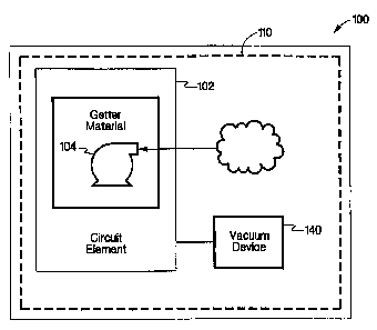
Fig. 1 is a block diagram of an electronic device according to an
embodiment of this invention;
Fig. 2 is a cross-sectional view of an electronic device according to an
embodiment of this invention;
Fig. 3 is a cross-sectional view of an electronic device according to an
embodiment of this invention;
Fig. 4 is a cross-sectional view of an electronic device according to an
embodiment of this invention;
Fig. 5 is a plan view of an electronic device according to an embodiment
of this invention;
Fig. 6 is a cross-sectional view of an electronic device according to an
embodiment of this invention;
. a . ];:~~ LI-C, , p~ I , ~I
10017445 CA 02390677 2002-06-14
4 --
Fig. 7 is a block diagram of an electronic device according to an
embodiment of this invention:
Fig. 8 is a flow diagram of a method of manufacturing an electronic device
according to an embodiment of this invention;
Fig. 9 is a flow diagram of a method of using an electronic device
according to an embodiment of this invention.
DETAILED DESCRIPTION
Referring to Fig. 1, an embodiment of electronic device 100 of the present
invention in a simplified block diagram is shown. Non-evaporable Better
material
104 is utilized as at least a portion of a circuit element 102. Getter
material 104,
thus, provides two functions; Better material 104 provides the Bettering
function
to maintain a vacuum (i.e. the trapping of reactive gas particles at a low
pressure) for vacuum device 140; in addition, Better material 104 also
provides
at least a portion of the electrical conduction function of circuit element
102
Unlike prior techniques, the present invention utilizes a portion of the
surface
area of substrate 110 that is already utilized for circuit elements for
Bettering as
well, thereby providing for either a reduction in the size of the device
substrate or
2o an increase in the surface area of Better material 104 or some combination
thereof. This is in marked contrast with prior techniques that use either a
separate compartment or dedicated area on the device, package, or substrate,
for Better material 104. The present invention may also provide for a more
uniform vacuum over the surface of substrate 110 by utilizing Better material
104
in multiple circuit elements 102 such as, for example, capacitors, resistors,
inductors, and even on electrical traces and shields. The uniformity of the
reduced pressure over substrate 110 will, for example, depend on the
particular
application of the device as well as the layout requirements for the
particular
design utilized.
It should be noted that the drawings are not true to scale. Further, various
parts of the active elements have not been drawn to scale. Certain dimensions
_ ~. I p .~1 l ~~ I ~I
CA 02390677 2002-06-14
10017445
have been exaggerated in relation to other dimensions in order to provide a
clearer illustration and understanding of the present invention. In addition,
although the embodiments illustrated herein are shown in two-dimensional views
with various regions having depth and width, it should be understood that
these
5 regions are illustrations of only a portion of a device that is actually a
three-
dimensional structure. Accordingly, these regions will have three dimensions,
including, length, width and depth, when fabricated on an actual device
Referring to Fig. 2, an exemplary embodiment of the present invention is
shown in a cross-sectional view. In this embodiment, vacuum device 240 is
disposed over at least a portion of substrate 210. Preferably, vacuum device
240 is an electron emitter device commonly referred to as either a Spindt tip
or a
flat electron emitter. Dielectric or insulating layer 220 is disposed over
substrate
210 and provides insulation between vacuum device 240 and electron lens 230.
Application of the appropriate signal to the electron lens generates the
necessary field gradient to focus electrons emitted from vacuum device 240 as
is
well known in the art. The present invention utilizes the conductive Better
material to generate the necessary field gradient to focus electrons, in
addition to
providing the Bettering of ambient gas particles to maintain the necessary
reduced pressure for operation of the electronic device.
Substrate 210 is preferably manufactured using a silicon water having a
thickness of about 300-700 microns. Next using standard semiconductor
processing steps, well known in the art, vacuum device 240 as well as other
logic
devices required for the electronic device are formed on substrate 210.
Although
preferably, substrate 210 is silicon. other materials may also be utilized,
such as,
for example, various glasses; aluminum oxide, polyimide, silicon carbide, and
gallium arsenide. Accordingly, the present invention is not intended to be
limited
to those devices fabricated in silicon semiconductor materials, but will
include
those devices fabricated in one or more of the available semiconductor
materials
and technologies well known in the art, such as thin-film-transistor (TFT)
technology using polysilicon on glass substrates.
.. .
CA 02390677 2002-06-14
~~~ 7~~J
s
Electron lens 230, preferably, is fabricated using a non-evaporable Better
material, however, depending upon the particular application of the electronic
device electron lens 230 may also be composed of more than one conductive
layer provided at least the top surface layer of electron lens 230 includes a
non-
evaporable Better material 104. Getter materials include titanium, zirconium,
thorium, hafnium, vanadium, yttrium, niobium, tantalum, and molybdenum.
Preferably, Better material 104 is a zirconium-based alloy such as Zr-AI, Zr-
V, Zr-
V-Ti, or Zr-V-Fe alloys, and more preferably Zr-V-Ti or Zr-V-Fe alloys because
of the lower activation temperatures used for these materials. Getter material
104 in electron lens 230 is preferably'appiied using conventional sputtering,
evaporation, or other vapor deposition techniques well known in the art.
However, other techniques such as electrophoresis, manual, or mechanical
application, including screen printing, sprays or suspensions of Better
material
104 in a suspending medium, can also be utilized.
In general, Better material 104 has a uniform thickness between about 0.1
to about 10 microns, preferably between about 0.5 microns to about 5.0
microns,
and more preferably between about 0.75 microns to about 1.25 microns. Getter
material 104 forms a "pump" where the area and volume of Better material 104
determines the capacity of the pump. Normally there is a passivation layer on
the
surface of Better material 104 when exposed to ambient conditions. However,
when heated to a sufficiently high temperature the passivation layer diffuses
into
the bulk of Better material 104 resulting in activation of Better material
104. This
process of activation forms a clean surface upon which additional material may
adsorb. Heating the electronic device in an oven, preferably, activates Better
material 104; however, radio frequency power (RF), laser power, or heat
generated by operation of the electronic device may also be used to activate
Better material 104. The actual temperature used for activation depends on the
particular composition of Better material 104 and is preferably in the range
of
about 250?C to about 450?C.
3o Dielectric layer 220 provides electrical insulation between electron lens
230 and vacuum device 240 and other circuit elements or logic devices disposed
in1. : ~I~ j~~ ~~ ~:. ~I ~ ~~ , ~ i
CA 02390677 2002-06-14
10017445
7
on substrate 210. In general, dielectric layer 220 will have a uniform
thickness
range between about 0.1 microns to about 10 microns. preferably the range is
about 2.5 microns to 7.5 microns and more preferably 5.0 microns. The
particular composition, method of deposition, and deposition conditions of
both
dielectric layer 220 and Better material 104 are optimized to minimize
residual
stress in the electronic device. Preferably, dielectric layer 220 is silicon
oxide
(SiXO,,), however, other dielectric materials such as silicon nitride, silicon
carbide,
aluminum oxide, boron nitride and dielectric materials as well as various
combinations thereof can be utilized as is well known in the art. For example,
dielectric layer 220 can include a first dielectric layer of silicon oxide
(SixOy)
disposed over substrate 210 with a second dielectric layer of silicon nitride
(SiXNy) disposed over the silicon oxide layer and a third dielectric layer of
silicon
carbide disposed over the silicon nitride layer.
An alternative embodiment of the present invention is shown in a cross-
sectional view in Fig. 3. In this embodiment, Better material 104, as
described in
Fig. 1, is utilized as at least a portion of second lens element 330 of the
electron
lens system. Typically, second lens element 330 acts as a ground shield,
although depending upon the particular application of the electronic device
second lens element 330 may be used as, for example, a focusing lens. In
addition, although Fig. 3 shows only a two lens structure comprising second
lens
element 330 and electron lens 332, other structures including multiple lens
elements may also be utilized depending on the particular spatial and temporal
electron emission properties desired for a given application. Vacuum device
340
is disposed over at least a portion of substrate 310. Both vacuum device 340
and substrate 310 may have similar properties and characteristics as that
described above and mown in Fig. 2. First insulating or dielectric layer 322
electrically isolates second lens element 330 from electron lens 332. Second
insulating layer 320 electrically isolates electron lens 332 from vacuum
device
340 similar to dielectric layer 120 shown in Fig. 2. Both insulating layer 320
and
first dielectric layer 322 are preferably made of the same material and may be
selected from any or the materials described for dielectric layer 120
described
10017445 ~ 02390677 2002-06-14
»
above and shown in Fig. 1. Electron lens 332 is fabricated using any of the
well-
known conductor technologies utilized in semiconductor processing. For
example, electron lens 332 may be formed using aluminum; tungsten, tantalum,
titanium nitride, copper, or gold to name a few. In general, electron lens 332
will
have a uniform thickness in the range from about 0.075 to about 0.7 microns,
and about 0.2 microns is preferable.
An alternate embodiment of the present invention is shown in a cross-
sectional view in Fig. 4. In this embodiment, a capacitor formed by top
electrode
430, bottom electrode 434, and capacitor dielectric layer 424 disposed over
substrate 410 wherein top electrode 430 utilizes Better material. Although
Fig. 4
depicts a planar construction utilizing a dielectric between two metal layers
other
capacitor structures, well known in the art may also be utilized. For example,
a
collector-base or emitter-base junction capacitor used in bipolar devices can
be
used where appropriate. Another example is a planar dielectric capacitor
wherein Better material 104 forms the top or upper electrode and a doped
semiconductor forms the bottom electrode with a dielectric layer interposed
between the two conductive layers. In addition, in the later example, the
metal
interconnection to the doped semiconductor layer may also be formed using a
Better material, provided the top metal surface is exposed to the vacuum
environment.
With reference to Fig. 4, substrate 410 is preferably manufactured using
a silicon wafer, although other substrates as described above may also be
utilized. Transistors 412 are represented in Fig. 4 as only a single layer to
simplify the drawing. Using semiconductor processing steps, well known in the
art, transistors 412 as well as other logic devices required for the
electronic
device are formed in substrate 410 and are typically realized as a stack of
thin
film layers. The particular structure of transistors 412 is not relevant to
the
invention, however some type of solid state electronic device is preferably
present, such as, metal oxide field effect transistors ~MOSFET), bipolar
junction
transistors {BJT), or other active semiconductor elements.
r , a It i,-ll- I. , ~, I II ;~ ; .
CA 02390677 2002-06-14
()~~ 7~~J
9
Dielectric layer 414 is disposed over transistors 412 as well as other logic
devices on substrate 410. Dielectric layer 414 provides electrical insulation
between the capacitor and transistors 412 as well as between vacuum device
440 and transistors 412. Preferably, dielectric layer 414 is silicon oxide,
however other dielectric materials as well as multiple layers may be used as
described above.
Conductive layer 436 is disposed over dielectric layer 414 and electrically
couples to electrical contact regions 437 of transistors 412 through via
openings
438 formed in the dielectric layer 414. Vacuum device 440 is disposed over a
portion of dielectric layer 414. Preferably, vacuum device 440 is an electron
emitter, however, devices such as a digital mirror device, digital micro mover
as
well as other devices utilized in field emission displays, atomic resolution
storage
systems and micro-electro-mechanical systems (MEMS) and micro-optical-
electro-mechanical systems (MOEMS) that are incorporated within a vacuum
package, maintained at a low pressure. Conductive layer 436 routes signals
from transistors 412 as well as other logic devices to vacuum device 440 and
may also be formed utilizing a Better material, especially those areas that
have a
top surface exposed to the low pressure environment. In addition, it is
preferable
where conductive layer 436 is composed of more than one conductive layer that
at least the top surface layer includes a Better material.
As shown in Fig. 4 vacuum seal 480 is disposed on substrate 410 and
cover 490 is affixed to vacuum seal 480 such that interspace region 494 is
maintained at a pressure of less than 10'3 torr. Preferably, interspace region
494
is maintained at a pressure of less than 10'5 torr. However, some devices that
fall within the scope of the present invention, for example, lasers or plasma
displays, may utilize a low pressure of inert high purity gases at pressures
less
than about 50 torr. Vacuum seal 480 can be made by a variety of techniques
including thermal compression, glass frit bonding, brazing, anodic bonding, as
well as other techniques.
Referring to Fig. 5 an alternate embodiment of the present invention is
shown in plan view. In this embodiment, Better material is, preferably,
[~. . I G~ ~L I , ~ [ . ~I ~ J i
CA 02390677 2002-06-14
10017445
incorporated into a number of different passive circuit elements that would
typically be found on electronic devices, however it may also be incorporated
into active circuit elements such as Schottky contacts and metal contacts to
transistors.
5 Disposed over substrate 510 are interdigitated capacitor electrodes 530
and 534, electrical trace 570, resistor 560, and inductor 550 each of which is
fabricated using a non-evaporable Better material. However, depending upon
the particular application of the electronic device each circuit element 550,
560,
and 570 may also be composed of more than one conductive layer.provided that
10 at least the top surface layer of each circuit element includes a non-
evaporable
Better material. For example if electrical trace 570 and portion of trace end
540
represents a power trace that carries a higher current, then depending upon
the
particular application, it may be advantageous to utilize a Better material
trace on
top of a metal layer such as an aluminum or gold trace that minimizes the
power
dissipation within the combined metal trace. In addition the composition,
thickness, and width may be chosen to also minimize the residual stress in the
circuit element. The thickness or width or both, of the electrical trace 570
and
portion of trace end 540 to may be increased to reduce power dissipation when
appropriate.
2o Although Fig. 5 shows resistor 560 as a serpentine resistor other resistor
structures well known in the art may also be utilized such as resistors formed
via
Better material acting as a contact to doped semiconductor in substrate 510.
The present invention essentially may utilize any circuit element that
contains a
metallization layer that is exposed to the low pressure environment as a
portion
of a Better pump. This would also include active elements such as Schottky
contacts, and gate metal contacts asjust two examples.
Fig. 6 is an exemplary embodiment of an electronic device having
integrated vacuum device 640 that includes anode surface 682 such as a display
screen or a mass storage device that is affected by electrons 684 when they
are
preferably formed into a focused beam 686. Anode surface 682 is held at a
predetermined disiance from second electron lens element 630. in this
i .,~-I:~~k-.~r~ ~~~ a ,
10017445 ~ 02390677 2002-06-14
embodiment integrated vacuum device 640 is shown in a simplified block form
and may be any of the emitter structures well known in the art such as a
Spindt
tip or flat emitter structure.
In this embodiment, Better material 104 is utilized as second lens element
630 of the electron lens system, wherein second lens element 630 acts as a
ground shield. Vacuum device 640 is disposed over at least a portion of
substrate 610. First insulating or dielectric layer 622 electrically isolates
second
lens element 630 from third lens element 634. Second insulating layer 620
electrically isolates .electron lens 632 from vacuum device 640 and third
insulating layer 624 electrically isolates third lens element 634 from
electron lens
632. Both the lens elements and dielectrics are all fabricated using materials
and processes well known in the art.
As a display screen, preferably an array of pixels (not shown) are formed
on anode surface 682, which further are preferably arranged in a red, blue,
green order, however, the array of pixels may also be a monochromatic color.
An array of emitters (not shown) are formed on substrate 610 where each
element of the emitter array has one or more integrated vacuum device acting
as
an electron emitter. Application of the appropriate signals to an electron
lens
structure including electron lens 632, third lens element 634, and second lens
element 630 generates the necessary field gradient to focus electrons 684
emitted from vacuum device 640 and generate focused beam 686 on anode
surface 682.
As a mass storage device, anode surface 682 preferably includes a
phase-change material or storage medium that is affected by the energy of
focused beam 686. The phase-change material preferably is able to change
from a crystalline to an amorphous state (not shown) by using a high power
level
of focused beam 686 and rapidly decreasing the power level of focused beam
686. The phase-change material is able to change from an amorphous state to a
crystalline state (not shown] by using a high power level of focused beam 686
and slowly decreasing the power level so that the media surface has time to
anneal to the crystalline state. This change in phase is utilized to form a
storage
I;1. i. ;I I II
CA 02390677 2002-06-14
10017445
12
area on anode surface 682 that may be in one of a plurality of states
depending
on the power level of focused beam 686 used. These different states represent
information stored in that storage area.
An exemplary material for the phase change media is germanium telluride
(GeTe) and ternary alloys based on GeTe. The mass storage device also
contains electronic circuitry (not shown) to move anode surface 682 in a first
and
preferably second direction relative to focused beam 686 to allow a single
integrated vacuum device 640 to read and write multiple locations on anode
surface 682. To read the data stored on anode or media surface 682, a lower-
energy focused beam 686 strikes media surface 682 that causes electrons to
flow through the media substrate 680 and a reader circuit (not shown) detects
them. The amount of current detected is dependent on the state, amorphous or
crystalline, of the media surface struck by focused beam 686.
Referring to Fig. 7, an exemplary embodiment of electronic device 700 of
the present invention in a simplified block diagram is shown. In this
embodiment
electronic device 700 may be a computer system, video game, Internet
appliance, terminal, MP3 player, or personal data assistant to name just a
few.
Electronic device 700 includes microprocessor 792, such as an Intel Xeon or
Pentium ProcessorT"" or compatible processor although other processors exist
and are well known in the art. Microprocessor 792 is connected to memory
device 796 that includes computer readable memory that is capable of holding
computer executable commands used by microprocessor 792 to control data or
inputloutput functions or both. Memory device 796 can also store data that is
manipulated by microprocessor 792. Microprocessor is also connected to either
storage device 794 or display 798 or both. Storage device 794 and display 798
contain an embodiment of the present invention as exemplified in earlier
described figures and text showing various circuit elements including getter
material 104 as well as vacuum devices 140 having electron emitters that are
focused. Preferably, the electron lens element exposed to the low pressure
environment such as second lens element 630 shown in Fig. 6 includes getter
m aterial 104.
fi. ~ ~ i,...~~, ~~~ ~ji I ~~ ~~ i ~.
luul/~~+J CA 02390677 2002-06-14
13
A method of manufacturing an electronic device is shown as a flow
diagram in Fig. 8, the electronic device utilizes a Better material as method
of
maintaining a low pressure and as a portion of a circuit element. In step 802
transistors and other logic elements are formed for those applications
requiring
such elements. Preferably, the transistors and logic elements are formed in a
silicon wafer having a thickness of about 300-700 microns. The logic elements
and transistors are, preferably, formed using conventional semiconductor
processing equipment. Although the substrate preferably is silicon, other
materials may also be utilized, such as, for example, various glasses,
aluminum
l0 oxide, polyimide, silicon carbide, and gallium arsenide. For example
transistors
and logic devices fabricated on glass substrates using polysilicon thin-film-
transistor (TFT) technology can be utilized.
In step 804 the Better layer is created on the substrate. The Better
material is preferably applied using conventional sputtering, evaporation, or
other vapor deposition techniques. However, other techniques such as
electrophoresis, manual, or mechanical application, including screen printing,
spays or suspensions of the Better material in a suspending medium, can also
be utilized. Getter materials include titanium, zirconium, thorium, hafnium,
vanadium, yttrium, niobium, tantalum, and molybdenum. Preferably, the Better
material is a zirconium-based alloy such as Zr-AI, Zr-V, Zr-V-Ti, or Zr-V-Fe
alloys, and more preferably Zr-V-Ti or Zr-V-Fe alloys because of the lower
activation temperatures used for these materials. In general, the Better
material
is formed as a uniform layer having a thickness between about 0.1 to about 10
microns, preferably between about 0.5microns to about 5.0 microns, and more
preferably between about 0.75 microns to about 1.25 microns. Patterning of the
Better layer is accomplished through any or' the photoiithographic and etching
technologies well known in the art.
In step 806 the circuit elements are formed on the substrate. As
described above a wide variety or' circuit elements and combinations of
elements
can be utilized in the present invention. Preferably, conventional
semiconductor
processing equipment can be utilized. For example, a resistor, a conductor
trace,
I~- , I Ii.ll I ;I~ I - Al ~~ I
CA 02390677 2002-06-14
10017445
14
an electron shield, or a metal contact to a doped region may be formed by
blanket deposition of the Better material on the substrate with subsequent
patterning and etching of the Better layer.
In step 808 the vacuum device is formed on the substrate. Preferably, the
vacuum device is formed by utilizing conventional semiconductor fab processes
and equipment. Typically the vacuum device is formed as a thick-film stack
that
utilizes etch selectivity between different layers, as well as etch stop
capability
and designs and deposition conditions that form low stress forces between the
layers as is well known in the art. For example, an electron emitter vacuum
device includes an electron supply layer that is preferably a heavily doped
semiconductor substrate such as silicon where the doping is preferably n-type
doping such as phosphorous, arsenic, or antimony. A tunneling layer is then
created on the surface of the electron supply layer and is preferably a thin
oxide
layer about 200 Angstroms thick. A cathode or electron emitter layer is then
applied over the surface of the tunneling layer. The electron emitter layer is
preferably formed from a deposition of platinum or optionally gold about 100
Angstroms thick.
In step 810 conductive traces are formed that couple the vacuum device
to various circuit elements such as transistors, capacitors, electron lens
structures to name a few. Preferably the conductive traces are formed using
the
Better material as described above. However, depending on the particular
application, the conductive traces or some portion thereof may include other
conductive materials. For example, metals, conductive inks, or organic
conductors such as thiophene compounds and other materials well known in the
art may also be utilized.
A method of using an electronic device utilizing a Better material as a
method of maintaining a low pressure and as a portion of a circuit element is
shown as a flow diagram in Fig. 9. In step 902 the Better material is
activated to
maintain a vacuum or reduced pressure. Preferably, the Better material is
activated by placing the electronic device in an oven and heating the device
and
Better material to a sufficient temperature tar a prescribed time. However,
radio
,. . I~ I,~.I~ '~ ~I I II I
10017445 CA 02390677 2002-06-14
frequency power (RF) or laser power also may be utilized to activate the
getter
material, as well as heat generated by operation of the electronic device may
also be used to activate the Better material. The time of heating depends on
the
particular Better material used and the temperature to which it is heated. The
5 higher the temperature typically the shorter the time required to activate
the
Better material.
In step 904 a circuit element is energized by applying an appropriate
signal through a portion of the Better material that forms at least an
electrical
portion of the circuit element. In step 906 a vacuum device is energized by
10 applying an appropriate signal through preferably a portion of the Better
material
that forms at least a portion of an electrical interconnection between a
circuit
element and the vacuum device.
While the present invention has been particularly shown and described
with reference to the foregoing preferred and alternative embodiments, those
15 skilled in the art will understand that many variations may be made therein
without departing from the spirit and scope of the invention as defined in the
following claims. This description of the invention should be understood to
include all novel and non-obvious combinations of elements described herein,
and claims may be presented in this or a later application to any novel and
non-
obvious combination of these elements. The foregoing embodiments are
illustrative, and no single feature or element is essential to all possible
combinations that may be claimed in this or a later application.
What is claimed is: