Language selection

Search

Patent 2391339 Summary

Third-party information liability

Some of the information on this Web page has been provided by external sources. The Government of Canada is not responsible for the accuracy, reliability or currency of the information supplied by external sources. Users wishing to rely upon this information should consult directly with the source of the information. Content provided by external sources is not subject to official languages, privacy and accessibility requirements.

Claims and Abstract availability

Any discrepancies in the text and image of the Claims and Abstract are due to differing posting times. Text of the Claims and Abstract are posted:

  • At the time the application is open to public inspection;
  • At the time of issue of the patent (grant).
(12) Patent: (11) CA 2391339
(54) English Title: EMAT TRANSMIT/RECEIVE SWITCH
(54) French Title: COMMUTATEUR D'EMISSION/RECEPTION POUR TRANSDUCTEUR ELECTROMAGNETIQUE ACOUSTIQUE (EMAT)
Status: Term Expired - Post Grant Beyond Limit
Bibliographic Data
(51) International Patent Classification (IPC):
  • G01N 29/04 (2006.01)
  • G01N 29/24 (2006.01)
  • G01N 29/34 (2006.01)
  • G01N 29/36 (2006.01)
  • H02J 03/06 (2006.01)
(72) Inventors :
  • MACLAUCHLAN, DANIEL T. (United States of America)
  • OVERBY, CHARLES B. (United States of America)
(73) Owners :
  • MCDERMOTT TECHNOLOGY, INC.
(71) Applicants :
  • MCDERMOTT TECHNOLOGY, INC. (United States of America)
(74) Agent: SMART & BIGGAR LP
(74) Associate agent:
(45) Issued: 2003-12-30
(86) PCT Filing Date: 2000-08-15
(87) Open to Public Inspection: 2001-03-01
Examination requested: 2002-01-25
Availability of licence: N/A
Dedicated to the Public: N/A
(25) Language of filing: English

Patent Cooperation Treaty (PCT): Yes
(86) PCT Filing Number: PCT/US2000/022447
(87) International Publication Number: US2000022447
(85) National Entry: 2002-01-25

(30) Application Priority Data:
Application No. Country/Territory Date
09/377,453 (United States of America) 1999-08-19

Abstracts

English Abstract


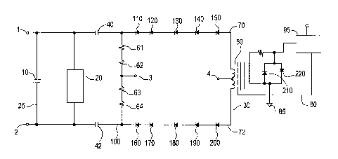
A transmitting and receiving switch assembly for an electromagnetic acoustic
transducer (EMAT) and a method for selectively switching an EMAT between
transmit mode and receive mode both use a particular circuit. This circuit
contains an EMAT coil (20) coupled to a tuning capacitor (10), which allows
the EMAT to be operated at a desired frequency when transmitting. A set of
capacitors (40, 42) separates the EMAT coil (20) from a set of diode strings
(70, 72) (preferably containing at least one fast switching diode), which are
joined by a resistive connection (61, 62, 63, 64). A transformer (50), which
is center tapped at its primary winding, is coupled to the other end of the
diode strings (70, 72). Finally, a receiver input (95) is connected to the
transformer (50). In operation, the frequency of the EMAT (20) is set by
appropriately energizing and tuning the tuning capacitor (10). A voltage is
then applied in the center tapped transformer (50) and in the resistive link
(61, 62, 63, 64) between the diode strings (70,, 72). The current
automatically switches the conductivity of the diodes and permits the EMAT
(20) to switch modes as desired. Likewise, the method disclosed also utilizes
this circuit, as described above, and involves several steps. First, the EMAT
frequency must be selected and set, using the tuning capacitor (10). Then, a
voltage is applied within the circuit to induce transmission by the EMAT (20).
Next a sinusoidal toneburst is given within the circuit to switch the
transmit/receive capabilities of the EMAT (20), and then observing the input
received by the EMAT (20) - thereby permitting the alternate switching of the
EMAT (20) from receive to transmit mode in a matter of nanoseconds.


French Abstract

L'invention concerne un ensemble commutateur d'émission/réception pour transducteur électromagnétique acoustique (EMAT), et un procédé de commutation sélective du mode d'émission au mode de réception du transducteur électromagnétique acoustique, dans lesquels on utilise un circuit particulier. Ce circuit contient une bobine (20) de transducteur électromagnétique acoustique couplée à une capacité d'accord (10), permettant au transducteur d'être exploité à une fréquence désirée lors de l'émission. Un ensemble de capacités (40, 42) sépare la bobine (20) du transducteur d'un ensemble de chaînes (70, 72) de diodes (contenant, de préférence, au moins une diode de silicium de commutation rapide), unies par une connexion résistive (61, 62, 63, 64). Un transformateur (50), à prise centrale au niveau de son bobinage primaire, est couplé à l'autre extrémité des chaînes (70, 72) de diodes. Enfin, une entrée (95) récepteur est connectée au transformateur (50). En fonctionnement, la fréquence du transducteur électromagnétique acoustique (20) est établie par une mise sous tension et un accord appropriés de la capacité d'accord (10). Une tension est alors appliquée au transformateur (50) à prise centrale, et à la connexion résistive (61, 62, 63, 64) entre les chaînes (70, 72) de diodes. Le courant commute automatiquement la conductivité des diodes et permet au transducteur électromagnétique acoustique (20) de passer d'un mode à l'autre comme désiré. De la même manière, le procédé de l'invention utilise également le circuit décrit ci-dessus, et comprend plusieurs étapes. En premier lieu, la fréquence du transducteur électromagnétique acoustique doit être sélectionnée et établie à l'aide de la capacité d'accord (10). Une tension est ensuite appliquée au circuit pour induire l'émission par le transducteur (20). Puis une rafale de fréquence sinusoïdale est générée dans le circuit, de façon à commuter les capacités d'émission/réception du transducteur (20). La surveillance de l'entrée reçue par le transducteur (20) permet ensuite d'assurer la commutation alternée du transducteur (20) du mode de réception au mode d'émission en quelques nanosecondes.

Claims

Note: Claims are shown in the official language in which they were submitted.


CLAIMS
We claim:
1. A transmitting and receiving switching circuit for an electromagnetic
acoustic
transducer (EMAT) comprising:
an EMAT coil;
a means for resonating the inductance and resistance of the EMAT coil at a
desired frequency, connected to the EMAT coil;
a first means for selectively redirecting an electrical current, connected to
the
EMAT coil;
a second means for selectively redirecting the electrical current, connected
to the
first means for selectively redirecting the electrical current;
a means for resisting the electrical current, connected to the first means for
selectively redirecting the electrical current and connected to the second
means for
selectively redirecting the electrical current;
a transformer, connected to the second means for selectively redirecting the
electrical current;
an input receiver for detecting electrical signals, having an input port and
connected to the transformer; and
a voltage, selectively applied to the transformer and to the means for
resisting the
electrical current.
2. A switching circuit according to claim 1, wherein the first means for
selectively
redirecting the electrical current comprises a plurality of capacitors.
3. A switching circuit according to claim 1, wherein the second means for
selectively redirecting the electrical current comprises a plurality of
diodes.
4. A switching circuit according to claim 2, wherein the second means for
selectively redirecting the electrical current is a plurality of diodes.
5. A switching circuit according to claim 3, wherein the diodes are fast
switching
silicon diodes.

-8-
6. A switching circuit according to claim 4, wherein the diodes are fast
switching
silicon diodes.
7. A switching circuit according to claim 1, wherein the means for resonating
the
inductance and resistance of the EMAT coil at a desired frequency comprises a
tuning
capacitor, connected to opposite ends of the EMAT coil, and the application of
a
controlled toneburst at opposite ends of the tuning capacitor.
8. A switching circuit according to claim 7, wherein the controlled toneburst
has a
voltage between 100 and 500 volts peak.
9. A switching circuit according to claim 1, wherein the input receiver
further
comprises a means for preventing large voltages from entering the input
receiver.
10. A switching circuit according to claim 9, wherein the means for preventing
large
voltages from entering the input receiver comprises a plurality of diodes
arranged in a
back-to-back configuration across the input port to the input receiver.
11. A method for selectively switching an electromagnet acoustic transducer
(EMAT)
circuit, having a tuning capacitor, a plurality of capacitors, a plurality of
diodes, a
plurality of resistors, a transformer, and an input receiver, between
transmitting mode and
receiving mode comprising:
applying an initial toneburst across the tuning capacitor and the EMAT coil;
resonating the inductance and resistance of the EMAT coil with the tuning
capacitor to a desired frequency;
selectively applying a voltage across the transformer, the plurality of
resistors,
and the plurality of diodes whereby a transmission signal in the EMAT is
produced;
selectively emitting a sinusodial toneburst across the plurality of diodes
whereby
the conductivity of the diodes is altered; and
selectively monitoring the signal received by the input receiver whereby a
receiving signal from the EMAT is detected.

-9-
12. A method according to claim 11, wherein the transformer includes a primary
winding and wherein the voltage is applied to the transformer at the center of
the primary
winding of the transformer and to the mid-point of the plurality of resistors.
13. A method according to claim 11, wherein the initial toneburst is between a
100
and 500 volt peak.

Description

Note: Descriptions are shown in the official language in which they were submitted.


CA 02391339 2002-O1-25
WO 01/14869 PCT/US00/Z2447
-1-
EMAT TRANSMIT/RECEIVE SWITCH
FIELD AND BA CKGRO UND OF THE INVENTION
Transmit/Receive (T/R) switches are used extensively in radio communications
electronics. In these applications, the T/R switch is used to couple an
antenna to the
transmitter and receiver electronics in a manner such that when transmitting,
the majority
of the transmitter power goes to the antenna and when receiving, the majority
of the
signal received by the antenna goes to the receiver. The T/R switch also
protects the
1 o receiver circuitry from being damaged by large transmitter signals through
limiting the
power that gets to the receiver input section. Several different kinds of
electronic circuits
have been employed to perform the T/R switch function.
U.S. Patent No. 4,637,065 to Ruppel discloses one type of T/R switch used in
radio communications circuits and contains a good description of the prior
art. These
types of T/R switch circuits utilize PIN diodes, giving rise to a long switch
over time of
several milliseconds, which is adequate for most radio communications
applications.
However, a T/R switch suitable for use with Electromagnetic Acoustic
Transducers
(EMATs) must be very fast acting; that is, capable of switching from transmit
mode to
receive mode in a few microseconds or less. Thus, a drawback to using these
type of T/R
switches for EMAT operation is that the time it takes for the circuit to
recover from the
transmit mode and then switch to the receive mode is too long.
Another method of coupling the transmitter and receiver to the same transducer
is
to attach the output of the transmitter directly to the transducer and attach
the input to the
receiver to the transducer via resistors. As illustrated in Figure 1, a back-
to-back diode
(CR11 and CR12) arrangement is placed at the input to the receiver to prevent
damage to
the receiver circuit from the large transmitter voltages with the current
being limited by
the resistors. This allows rapid switching from transmit mode to receive mode.
SURSThfUTE SHEET (RULE 26)

CA 02391339 2002-O1-25
WO 01/14869 PCT/US00/Z2447
_2_
However, the use of resistors to couple the transducer to the receiver input
results in
transmit power loss in the resistors and signal to noise reduction from the
receiver
because of the increased resistance at the receiver input, so that this
arrangement is not
well-suited for use with EMATs.
Figure 2 illustrates another T/R switch circuit known to the inventor prior to
the
current invention. In this T/R switch, the transmitter output is coupled
directly to the
transducer. The transducer is then coupled to the receiver input via a power
limiting
circuit formed by diodes CR1 and CR2, inductor Ll, resistor R1, voltage source
Vl, and
transformer T1. Direct current (D.C.), supplied from V1 and limited by
resistor Rl,
to flows through the diodes CR1 and CR2. This D.C. is set by R1 such that the
diodes are
biased "on" for small signals; that is, a small received signal passes from
the transducer
to the receiver input unimpeded because the diodes are put into a conductive
state (low
resistance) by the D.C. bias currents. Inductor L1 provides a high impedance
for the
radio frequency (RF) signals preventing them from flowing through voltage
source V 1.
High voltage RF signals applied to the transducer cause the diodes to become
reverse
biased, switching them into a nonconductive state. This switching time depends
on what
diodes are employed in the circuit.
In the circuit illustrated in Figure 2, the diodes employed had switching
times on
the order of 1/10 of a microsecond. However, the 1/10 of a microsecond
switching time
limited the operation to frequencies below approximately 2 MHz because the
diodes must
switch on and off with each cycle of the transmitter RF toneburst.
Consequently, one
disadvantage to using this circuit for EMAT operation is that it is single
ended (one side
of the transducer is connected to ground), and those skilled in the art have
found that, in
order to prevent noise pickup, the EMAT coil is best kept isolated from ground
and
operated into a differential input receiver which provide high common mode
noise
rejection. Likewise, the D.C. bias current flowing through the primary
windings of T1
can cause the transformer core to saturate if it is not of adequate size
resulting in larger
transformer size than would otherwise be necessary. Therefore, the circuit
illustrated in
Figure 2 is not well-suited for use with EMATs.
In sum, it is apparent that an improved T/R switch suitable for use with an
EMAT
is needed to overcome the deficiencies discussed above. Moreover, such an
improved
T/R switch for use with an EMAT would be welcome by the industry.

CA 02391339 2002-O1-25
WO 01/14869 PCT/US00/22447
-3-
SUMMARY OF THE INVENTION
The present invention seeks to improve the T/R switching capabilities during
EMAT operation. Specifically, the T/R switch disclosed in the present
invention
provides several advantages for EMAT operation. This circuit blocks the
transmitter
pulses from being sent to the input to the receiver, while allowing the small
received
signals to be applied to the input to the receiver with very little
attenuation or added
source resistance. Additionally, since this circuit is balanced with respect
to ground,
good common mode noise rejection is obtained.
Assuming that the input impedance is infinite, the use of resistors to couple
the
to received signal from the EMAT to the input to the receiver reduces the
signal to noise
ratio by a factor of two, as compared to an ideal T/R switch. That is, in
prior art circuits,
the input impedance of the receiver may actually be low enough, especially at
high
frequencies, to produce significant attenuation of the received signals if
resistors are
placed between the transducer and the receiver input. In lab testing of the
present
invention, an improvement in signal to noise of a factor of three was observed
when this
T/R switch was substituted for resistor coupling between the transducer and
the EMAT
receiver during operation at SMHz. In many applications, these improvements in
signal
to noise ratio can mean the difference between being able to perform the test
and not
being able to perform the test.
Also, receiver input transformer core saturation is prevented in the present
invention by using a center tapped primary with the bias current flowing in
opposite
directions in each half of the primary windings. This use of a center tapped
primary
allows very small receiver input transformers to be constructed.
One aspect of the present invention is drawn to an improved electrical circuit
which utilizes an EMAT as both a transmitter and a receiver by allowing the
fast
switching of the EMAT from transmit to receive mode, and vice versa. In
addition to an
EMAT coil, this circuit contains a tuning capacitor which allows the EMAT to
be
operated at a desired frequency when transmitting. The EMAT is also coupled to
a pair
of capacitors which are, in turn, connected to two separate diode strings. The
diode
3o strings preferably contain at least one fast switching silicon diode,
although the use of
similar diodes is possible. The diode strings are also resistively connected
to each other at
their respective junctions with the capacitors. The other end of each diode
string is

CA 02391339 2002-O1-25
WO 01/14869 PCT/US00/22447
-4-
coupled to a single transformer, which is center tapped at its primary
winding. Finally,
the transformer is coupled to an input receiver.
In operation, the frequency of the EMAT is set by appropriately energizing and
tuning the tuning capacitor. A voltage is then applied in the center tapped
transformer
and in the resistive link between the diode strings. The current automatically
switches
the conductivity of the diodes and permits the EMAT to switch modes as
desired.
Another aspect of the present invention is drawn to an improved method for
selectively switching an EMAT between transmitting mode and receiving mode.
Essentially, this method utilizes a circuit, as described above, and involves
several steps.
1o A sinusodial toneburst voltage is applied across the terminals of the EMAT
coil to induce
transmission by the EMAT. The large applied voltages reverse bias the diode
strings,
effectively switching off the input to the receiver section. When the
transmitter voltage is
turned off, the diodes are biased on by the current supplied by D.C. power
source through
current limiting resistors, effectively turning on the input to the receiver
section.
The various features of novelty which characterize the invention are pointed
out
with particularity in the claims annexed to and forming a part of this
disclosure. For a
better understanding of the invention, its operating advantages, and the
specific objects
attained by its uses, reference is made to the accompanying drawings and
descriptive
matter in which the preferred embodiments of the invention are illustrated.
2o
BRIEF DESCRIPTION OF THE DRA WINGS
In the drawings:
Figure 1 is a schematic representation of a first known T/R switch;
Figure 2 is a schematic representation of a second known T/R switch; and
Figure 3 is a schematic representation of an improved T/R switch for use with
an
EMAT, according to the preferred embodiment of the present invention.
DESCRIPTION OF THE PREFERRED EMBODIMENTS
Referring to the drawings generally, wherein like numerals designate the same
or
3o functionally similar elements throughout the several drawings, and to
Figure 3, in
particular, there is shown a schematic diagram of the preferred embodiment of
the
invention. The T/R circuit 100 is a fast switching, balanced, transmitting and
receiving
switch with good common mode noise rejection for use with EMAT transducers. In

CA 02391339 2002-O1-25
WO 01/14869 PCT/US00/22447
-5-
operation, a large RF toneburst ( 100 to 500 volts peak) is applied at point 1
and point 2 in
T/R circuit 100. Tuning capacitor 20 is used to resonate the inductance and
resistance of
EMAT coil 20 to the desired operating frequency. This tuned tank circuit 25,
formed by
EMAT coil 20 and tuning capacitor 10, is energized by an applied transmitter
toneburst.
Large RF currents flow in the tank circuit 25 and, therefore in EMAT coil 20.
In turn, the
RF current flow then launches ultrasonic signals in the workpiece in the
presence of a
magnetic field (not shown).
The T/R switching circuit 30 is formed by capacitor 40, capacitor 42, resistor
61,
resistor 62, resistor 63, resistor 64, diode string 70, diode string 72, and
transformer 50.
1o Diode string 70 is formed by diode 110, diode 120, diode 130, diode 140,
and diode 150.
Diode string 72 is formed by diode 160, diode 170, diode 180, diode 190, and
diode 200.
Transformer 50 is preferably constructed with an electrostatic shield under
the primary
windings connected to the receiver ground, although the circuit can function
adequately
without such a shield. Input receiver circuit 80 includes diode 210, diode
220, and
receiver input 95. The differential input receiver is also connected to
transformer 50 and
a grounded fixture 85. The T/R switching circuit 30 is balanced with respect
to ground,
providing high common mode noise rejection. Balancing with respect to ground
is a well
known method of preventing common mode noise on the primary windings from
being
capacitively coupled to the secondary windings.
A voltage source is applied to point 3 and point 4. Current flows through the
center-tapped primary winding on transformer 50. Since this current flows in
opposite
directions in the two halves of the center tapped primary winding, this DC
current will
not produce saturation of the core of transformer 50. The current then flows
through
diode string 70 on one side of the T/R switching circuit 30 and diode string
72 on the
other side of the T!R switching circuit 30. However, this DC bias current is
blocked by
capacitor 40 and capacitor 42. Therefore, the current flows through resistor
61, resistor
62, resistor 63, and resistor 64, and then back to the power source. Capacitor
40 and
capacitor 42 are chosen so that they are a very low impedance at the desired
operating
frequency.
3o During reception, a small signal induced on the EMAT coil 20 is coupled,
via
capacitor 40, capacitor 42, "on-biased" diode string 70, and "on-biased" diode
string 72,
to the primary winding of transformer 50. (Note: The transmitter output is in
a high
impedance state when not transmitting, thereby preventing the transmitter
output from

CA 02391339 2002-O1-25
WO 01/14869 PCT/US00/22447
-6-
loading down the received signals.) Diode 210 and diode 220 are connected back
to back
across the input to the receiver circuit 80, thereby preventing large voltages
from being
generated at the input to input receiver 95 which might damage it.
During transmission, the large transmitter voltages applied to the T/R circuit
100
cause all the diodes in this circuit to be reverse-biased. A sinusoidal
toneburst alternately
reverse-biases diode string 70 and then diode string 72 as the voltage
reverses polarity.
Accordingly, all of the diodes then switch from conductive to nonconductive
states
within a few nanoseconds, as the applied voltage passes through zero and then
reverse-
biases diode string 70 and diode string 72. Consequently, all the diodes are
switched into
1 o a nonconductive state, thereby preventing the large transmitter power from
being applied
to the primary windings of transformer 50. As soon as the transmitter voltage
stops, the
circuit is then ready to pass the smaller received signals to the receiver
with very little
attenuation.
The diodes employed in this circuit are very fast switching silicon diodes,
although other types may also be used. These diodes switch in only a few
nanoseconds,
however their breakdown voltage is only about 100 volts each. Several diodes
are used
in the diode strings to increase the breakdown voltage to withstand the
transmitter voltage
when reverse biased.
While specific embodiments of the invention have been shown and described in
detail to illustrate the specific application of the principles of the
invention, it will be
understood that the invention may be embodied as more fully described in the
claims, or
as otherwise understood by those skilled in the art, without departing from
such
principles.

Representative Drawing
A single figure which represents the drawing illustrating the invention.
Administrative Status

2024-08-01:As part of the Next Generation Patents (NGP) transition, the Canadian Patents Database (CPD) now contains a more detailed Event History, which replicates the Event Log of our new back-office solution.

Please note that "Inactive:" events refers to events no longer in use in our new back-office solution.

For a clearer understanding of the status of the application/patent presented on this page, the site Disclaimer , as well as the definitions for Patent , Event History , Maintenance Fee  and Payment History  should be consulted.

Event History

Description Date
Inactive: Expired (new Act pat) 2020-08-17
Common Representative Appointed 2019-10-30
Change of Address or Method of Correspondence Request Received 2018-01-12
Inactive: Late MF processed 2015-12-08
Letter Sent 2015-08-17
Inactive: IPC from MCD 2006-03-12
Grant by Issuance 2003-12-30
Inactive: Cover page published 2003-12-29
Inactive: Final fee received 2003-10-14
Pre-grant 2003-10-14
Notice of Allowance is Issued 2003-09-19
Letter Sent 2003-09-19
Inactive: Approved for allowance (AFA) 2003-08-28
Letter Sent 2003-03-14
Amendment Received - Voluntary Amendment 2003-02-10
Inactive: Single transfer 2003-01-24
Inactive: Cover page published 2002-08-20
Inactive: Courtesy letter - Evidence 2002-08-20
Letter Sent 2002-08-14
Inactive: Notice - National entry - No RFE 2002-08-13
Application Received - PCT 2002-08-09
National Entry Requirements Determined Compliant 2002-01-25
Request for Examination Requirements Determined Compliant 2002-01-25
All Requirements for Examination Determined Compliant 2002-01-25
Application Published (Open to Public Inspection) 2001-03-01

Abandonment History

There is no abandonment history.

Maintenance Fee

The last payment was received on 2003-07-18

Note : If the full payment has not been received on or before the date indicated, a further fee may be required which may be one of the following

  • the reinstatement fee;
  • the late payment fee; or
  • additional fee to reverse deemed expiry.

Patent fees are adjusted on the 1st of January every year. The amounts above are the current amounts if received by December 31 of the current year.
Please refer to the CIPO Patent Fees web page to see all current fee amounts.

Owners on Record

Note: Records showing the ownership history in alphabetical order.

Current Owners on Record
MCDERMOTT TECHNOLOGY, INC.
Past Owners on Record
CHARLES B. OVERBY
DANIEL T. MACLAUCHLAN
Past Owners that do not appear in the "Owners on Record" listing will appear in other documentation within the application.
Documents

To view selected files, please enter reCAPTCHA code :


To view images, click a link in the Document Description column (Temporarily unavailable). To download the documents, select one or more checkboxes in the first column and then click the "Download Selected in PDF format (Zip Archive)" or the "Download Selected as Single PDF" button.

List of published and non-published patent-specific documents on the CPD .

If you have any difficulty accessing content, you can call the Client Service Centre at 1-866-997-1936 or send them an e-mail at CIPO Client Service Centre.

({010=All Documents, 020=As Filed, 030=As Open to Public Inspection, 040=At Issuance, 050=Examination, 060=Incoming Correspondence, 070=Miscellaneous, 080=Outgoing Correspondence, 090=Payment})


Document
Description 
Date
(yyyy-mm-dd) 
Number of pages   Size of Image (KB) 
Representative drawing 2002-08-18 1 6
Abstract 2002-01-24 1 74
Claims 2002-01-24 3 88
Description 2002-01-24 6 320
Drawings 2002-01-24 2 27
Reminder of maintenance fee due 2002-08-12 1 114
Notice of National Entry 2002-08-12 1 208
Acknowledgement of Request for Examination 2002-08-13 1 177
Request for evidence or missing transfer 2003-01-27 1 102
Courtesy - Certificate of registration (related document(s)) 2003-03-13 1 130
Commissioner's Notice - Application Found Allowable 2003-09-18 1 159
Maintenance Fee Notice 2015-09-27 1 170
Late Payment Acknowledgement 2015-12-07 1 163
PCT 2002-01-24 7 285
Correspondence 2002-08-12 1 24
Fees 2003-07-17 1 30
Correspondence 2003-10-13 1 33
Fees 2002-07-17 1 33