Note: Descriptions are shown in the official language in which they were submitted.
CA 02391442 2005-10-04
LARGE CURRENT WATCHDOG CIRCUIT FOR A PHOTODETECTOR
FIELD OF THE INVENTION
This invention relates to a current limiting circuit and more particularly a
circuit
which limits the amount of charge flowing in a photodetector such as an
avalanche
photodiode to prevent damage thereof and also to prevent damage to any front
end
sensing electronics.
BACKGROUND OF THE INVENTION
A photodetector is a device that converts light intensity into an electrical
signal.
The three most common types of photodetectors are photodiodes, avalanche
photodiodes,
and photomultiplier tubes. The first two types of photodetectors are
semiconductor
devices that detect low levels of electromagnetic radiation (photons) and are
constructed
so that a photon dislodges an electron (primary electron) and creates a hole-
electron pair.
These holes and electrons move in the opposite direction in the semiconductor
device
due to the electrical field that is applied across the photodiode. This
movement of
electrons through the structure is called photocurrent and it is proportional
to the light
intensity. In avalanche photodiodes, the primary electron hits other atoms
with sufficient
velocity and energy in the lattice structure to create additional electron-
hole pairs. This
cascade effect in avalanche photodiodes results in an effective gain and
allows the
detection of very low light levels. Indeed, single photon detection is
possible using an
avalanche photodiode combined with an active quench circuit. This type of
operation of
CA 02391442 2005-10-04
2
an avalanche photodiode is called the Geiger mode when the avalanche
photodiode is
biased above its breakdown voltage. Three examples of active quench circuits
are shown
in U. S. Patent Nos. 5,532,474; 5,933,042; and 4,945,277.
A photomultiplier tube type photodetector includes a cascade of dynodes in a
vacuum tube that converts photons into electrons and the multiplication effect
of the
primary photon electron creates the necessary electrical gain.
Under normal operating conditions, photodetectors are biased below the
breakdown voltage and the photocurrent is relatively small. In most of these
applications, front end sensing electronics including, inter alia, an
amplifier circuit is
required to convert the photocurrent of the photodetector to a voltage level
above the
background noise of the following stage electronics. The resulting voltage
signal is
indicative of the light intensity striking the photodetector.
In all photodetector applications, damage would occur if the photocurrent
induced
by errant light exceeds the front end sensing electronics limited breakdown
level. Errant
light can strike the photodetector, for example, when a laser is in close
proximity to the
photodetector and laser light scatters and is directed at the photodetector.
Decreasing the
susceptibility of the front end sensing electronics to high photocurrent
values is not an
easy task and most of the time it leads to performance degradation including
noise and
degraded speed. In any case, improving the front end sensing electronics does
not protect
the photodetector itself which can sustain only a limited photocurrent prior
to permanent
damage.
In many applications, like Light Detection and Ranging (LIDAR), fluorescence,
and particle sizing, a powerful laser is used in conjunction with one or more
photodetectors. In these applications, errant back reflections of the laser
light into the
CA 02391442 2005-10-04
photodetector is frequently a problem that can saturate the photodetector
causing
permanent damage. It has been demonstrated in the laboratory that the
threshold for
permanent damage in a commercial active quench avalanche photodiode is around
1
million photons within one nanosecond causing a photodiode current in excess
of twenty
miliamps. Lasers used in conjunction with many photodetector applications
generate
light levels many orders of magnitude above this permanent damage threshold.
Thus, the
need to quickly stop the photodiode current surge induced by errant light
laser is
mandatory in low light level detection applications such as single photon
detection to
avoid destruction of the photodiode.
One prior art way to limit the photodiode current is to use a high ohm (e. g.,
a
kilo-ohm or higher) resistor in series with the photodetector. This approach
has several
limitations. Due to Ohm's law, the current in this high ohm resistor creates a
voltage
drop across the resistor even in the normal operating mode of the photodiode
which
reduces the bias voltage across the photodiode. This voltage drop decreases
the
photo-detection efficiency of the photodiode since the light detection
efficiency of the
photodetector is directly related to the bias voltage across the detector. On
the other
hand, the use of a smaller resistor would not adequately protect the
photodiode.
Also known in the art is a clipper circuit used to protect the front end
sensing
CA 02391442 2002-05-13
WO 02/23690 PCT/USO1/28418
4
electronics against high photodetector currents caused by errant light
sources. The
clipper circuit, however, does not limit the photodetector current and thus
does not
protect the photodetector against high photodetector currents.
SUMMARY OF THE INVENTION
It is therefore an object of this invention to provide a current limiting
watchdog
circuit for photodetectors including photodiodes, avalanche photodiodes, and
photomultiplier tubes.
It is a further object of this invention to provide a watchdog current
limiting
circuit which can withstand high errant light levels without degradation of
the
photodetector or the front end sensing circuitry.
It is a further obj ect of this invention to provide a watchdog current
limiting
circuit which limits the current flowing in the photodetector to avoid its
destruction.
It is a further object of this invention to provide a watchdog current
limiting
circuit which does not affect the detection efficiency of the photodetector in
its normal
operating region.
It is a further object of this invention to provide a watchdog current
limiting
circuit which does not affect the input impedance of the front end sensing
electronics
attached to the output of the photodetector.
It is a further obj ect of this invention to provide a watchdog current
limiting
circuit which operates independently of the supply voltage level applied to
the
photodetector.
This invention results from the realization that by connecting the source of a
transistor to a sensing resistor which monitors the photodetector current and
CA 02391442 2002-05-13
WO 02/23690 PCT/USO1/28418
connecting the drain of the transistor to the photodetector, then the
drain/current
resistance of the transistor can be increased to the transistor's saturation
point to
protect the photodetector from high currents caused by errant light sources
but only
when the photodetector current reaches a trigger point to thus maintain the
detection
efficiency of the photodetector below the trigger point where the drain/source
resistance of the transistor is very low. In the preferred embodiment, the
gate of the
transistor is connected to a bias voltage so that the transistor gatelsource
voltage
decreases to drive the transistor drain/source resistance up as the
photodetector
current increases. Also in the preferred embodiment, the bias voltage is
independent
of the polarization voltage applied to the photodetector.
This invention features a large current watchdog circuit for a photodetector.
The watchdog circuit comprises a current sensing device responsive to current
flowing
through the photodetector; and a variable impedance element responsive to the
current
sensing device and the photodetector which increases in resistance in response
to
current flowing through the photodetector to protect the photodetector from
high
current levels.
In one example, the photodetector is a photodiode. One current sensing
device is a resistor connected between the voltage supply source and the
photodetector. In the same example, the variable impedance element is a
transistor
having its drain connected to the photodetector and its source connected to
the
resistor thus providing a drain/source resistance which varies in response to
the
current flowing through the photodetector. The gate of the transistor is
connected to
a bias voltage source. The bias voltage source may include a capacitor for
holding
the voltage at the gate of the transistor steady and a resistor in parallel
with the
CA 02391442 2002-05-13
WO 02/23690 PCT/USO1/28418
6
capacitor. In the preferred embodiment, the bias voltage source draws voltage
from
the supply voltage source and includes a plurality of diodes interconnected
between
the supply voltage source and the gate of the transistor.
In another embodiment, the bias voltage source includes a Zener diode
interconnected between the supply voltage source and the gate of the
transistor. In
still another example, the bias voltage source is a battery.
In the preferred embodiment, the watchdog circuit comprises a photodetector
connected to a supply voltage source; a sensing resistor connected between the
supply
voltage source and the photodetector; a bias voltage source; and a transistor
having its
source connected to the sensing resistor, its drain connected to the
photodetector, and
its gate connected to the bias voltage source such that the drain/source
resistance
increases when the gate/source voltage decreases to thereby protect the
photodetector
from large currents.
In the broader sense, there is a photodetector connected to a voltage supply
source; a variable impedance connected between the supply voltage source and
the
photodetector; and a variable voltage responsive to the photodetector current
to drive
the variable impedance up as the photodetector current increase. In the
typical case,
the variable impedance is the source and drain of a transistor connected
between the
voltage supply source and the photodetector. A resistor is then connected
between
the source of the transistor and the voltage supply source and the variable
voltage is
the gate and source of the transistor, the gate comiected to a bias voltage
source, the
source connected between the photodetector and the resistor.
Also in the preferred embodiment, the watchdog circuit includes a
photodetector connected to a voltage supply source; a bias voltage source; and
a
CA 02391442 2002-05-13
WO 02/23690 PCT/USO1/28418
7
transistor having its source and drain interconnected between the
photodetector and
the voltage supply source and its gate connected to a bias source operating to
keep
the transistor on, the transistor having a low value source/drain resistance
(e.g., 850
ohms) when the photodetector current is at nominal levels (e.g., 20 miliamps),
so
that the operation of the photodetector is not affected. The transistor
becomes
saturated, however, when the photodetector current exceeds the nominal levels,
and
then has a high source/drain resistance value (e.g., infinity) to protect the
photodetector from high level current values. In one specific example, the
transistor
impedes photocurrent values above about 20 miliamps but has only an 85 olun
source/drain resistance when the photodocument is below 20 miliamps such that
even avalanche photodiodes operated in the Geiger mode are not adversely
affected
by the watchdogs circuit when the photocurrent is below this nominal level.
BRIEF DESCRIPTION OF THE DRAWINGS
Other objects, features and advantages will occur to those skilled in the art
from the following description of a preferred embodiment and the accompanying
drawings, 11 WhlCh:
Fig. 1 is a schematic view of a prior art watchdog circuit for a photodetector
employing a high ohm resistor;
Fig. 2 is a circuit diagram of a prior art clipper circuit used to protect the
front
end sensing electronics coupled to a photodetector against high photodetector
current
levels;
Fig. 3 is a schematic block diagram depicting the primary components
associated with the watchdog circuit of the subject invention;
CA 02391442 2002-05-13
WO 02/23690 PCT/USO1/28418
Fig. 4 is a circuit diagram showing one embodiment of the large current
watchdog circuit for a photodetector in accordance with the subject invention;
Fig. 5 is a circuit diagram showing an alternative embodiment of the bias
voltage source shown in the circuit of Fig. 4;
Fig. 6 is a circuit diagram showing another embodiment of the bias voltage
source shown in the circuit of Fig. 4;
Fig. 7 is a circuit diagram depicting another embodiment of the large current
watchdog circuit for a photodetector in accordance with the subject invention;
and
Fig. 8 is a graph showing a typical photodetector current saturation level
versus the voltage between the gate and the source of the transistor used in
the
preferred embodiment of the subject invention and also the typical
photodetector
current saturation versus the load line of the sensing resistor in accordance
with the
preferred embodiment of the subject invention.
DISCLOSURE OF THE PREFERRED EMBODIIVVIENT
As discussed in the background section above, a typical photodetector such
as photodiode 12, Fig. 1 is connected to voltage supply source 14 and, when
light 15
strikes photodetector 12, it outputs a photodiode current (photocurrent)
proportional
to the intensity of light 15 incident thereon. This photodiode current is then
amplified and converted to a voltage or other signal by front end electronics
16 and
provided to output 18. The resulting output signal is indicative of the
incident light
level or, in the case of avalanche photodiodes, the presence of a single
photon
striking photodiode 12.
When, however, the incident light level is too high, such as from a laser
CA 02391442 2002-05-13
WO 02/23690 PCT/USO1/28418
9
which scatters errant light in the direction of photodiode 12 as shown at 13,
the
resultant in photodiode current can destroy photodiode 12 and also adversely
affect
front end sensing electronics 16.
In the prior art, high ohm resistor 20 (typically thousands of ohms) impedes
any high photodiode current levels caused by errant light 13. Unfortunately,
high
ohm resistor 20 also causes a bias voltage drop across photodiode 12 reducing
its
sensitivity and efficiency.
It is also known in the art to include clipper circuit 30, Fig. 2 including
diode
32, resistors 34 and 36 and capacitor 38 to protect front end sensing
electronics 16
from high photodiode current levels. As delineated in the background section
above,
however, clipper circuit 30 does not protect photodiode 12 from damage caused
by
high photodiode current levels resulting from errant light incident thereon.
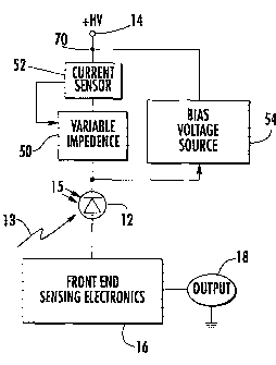
In this invention, a photodetector such as photodiode 12, Fig. 3 is protected
against high photodiode current levels by the inclusion of variable impedance
50
between photodiode 12 and current sensor 52. Variable impedance 50 is low,
e.g. 85
ohms, during the normal operation of photodetector 12. When, however, current
sensor 52 senses a photodiode current in excess of a predetermined threshold
(e.g.,
20 miliamps), due to errant light 13, the impedance of variable impedance 50
is
driven up to protect photodiode 12. In the preferred embodiment, the high
impedance value for variable impedance 50 can be thought of as infinite
impedance.
After the errant light shown at 13 is removed, however, the impedance of
variable
impedance 50 returns to its low impedance value and photodiode 12 then
operates in
a normal manner. Thus, only when the photodetector current level reaches a
trigger
point does variable impedance 50 provide a large resistance. Bias voltage
source 54
CA 02391442 2002-05-13
WO 02/23690 PCT/USO1/28418
sets the trigger point and defines the maximum photocurrent limit. At all
other
times, for example, before the trigger point is reached and after the
photodetector
current falls below the trigger point, the resistance of variable impedance 50
is low
to thus maintain the detection efficiency of the photodetector. This result is
not
possible in the prior art circuit shown in Fig. 1 since resistor 20 is fixed
at a high
resistance value.
In the preferred embodiment, variable impedance element 50, Fig. 3 is the
resistance between source 64, Fig. 4 and drain 62 of Field Effect Transistor
68 which
varies in proportion to the gate 66/source 64 voltage. Current sensor 52, Fig.
3 in
this embodiment, is low ohm resistor 60, Fig 4 (e.g., 100 ohms) connected
between
voltage supply source 14 and photodiode 12. Bias voltage source 54, Fig. 3,
connected to gate 66, Fig. 4 of transistor 68, in this particular example,
includes the
combination of tap 70 to voltage supply source 14, a string of diodes 72, and
capacitor 74 in parallel with resistor 76.
Thus, the present invention features a small series resistance when
photodiode I2 is operating in its safe region but the resistance quickly
switches to a
high resistance value when the current flowing through photodiode 12 reaches a
predefined trigger point. By carefully setting this trigger point below the
damage
current threshold of the photodetector used and/or the damage current
threshold of
front end sensing electronics 16, neither the detector nor the sensing
electronics is
adversely affected when a high intensity current is generated by errant light
levels as
shown at 13. In other words, the quick transition from a low to high impedance
protects the photodetector against intense light levels but without degrading
the
performance of the photodetector in normal light level operating conditions.
The
CA 02391442 2002-05-13
WO 02/23690 PCT/USO1/28418
11
photodetector trigger point of the watchdog circuit can be uniquely set by the
bias
voltage source 54 and the resistor 60 combination for any particular detector.
Referencing the bias voltage source 54 to voltage supply 14 via the node 70
provides
the independence of this invention to any operating voltage of the
photodetector 12.
Thus the invention exhibits the flexibility required to match the requirements
of all
the various operating conditions of different types of photodetector devices:
photodiodes, avalanche photodiodes, and photomulitplier tubes.
In Fig. 4, the current sensing element in the form of resistor 60 monitors the
current flowing in photodetector 12. A variable impedance element in the form
of
transistor 68 is controlled by the sensing element to limit the current in the
photodiode. A biasing element in the form of capacitor 74 (e.g., l OnF)
maintains a
constant offset voltage in reference to the photodiode bias voltage on the
control
input of the sensing element.
In the preferred embodiment, bias voltage source 54 biases the watchdog
circuit and the photodetector. Low value resistor 60 in series with the
photodetector
acts as a sensing element of the current that flows through the photodetector.
Variable impedance element 68 in series with the photodetector and the sensing
element is, in this example, a Field Effect Transistor and the gate/source
voltage of
this Field Effect Transistor is used as the input that controls the impedance
value.
The constant offset, in reference to the photodetector bias voltage, is
created by the
voltage drop across the series of multiple diodes 72. Resistor 76 (e.g., lmS2)
is used
to ensure a direct current path for the diodes. Decoupling capacitor 74 to the
common voltage reference node (e.g., ground) maintains the offset constant.
This invention, however, is not limited to the particular bias voltage source
CA 02391442 2002-05-13
WO 02/23690 PCT/USO1/28418
12
shown in Fig. 4. Other examples include bias voltage source 54', Fig. 5 and
bias
voltage source 54", Fig. 6. Bias voltage source 54', Fig. 5 includes Zener
diode 80
which, it should be noted, draws more current from node 70 then the string of
diodes
shown in Fig. 4. Bias voltage source 54", Fig. 6, includes constant bias
voltage
source 82 such as a battery.
Also, in Fig. 4, transistor 68 is a P-type Field Effect Transistor (Part No.
VPO550). In Fig. 7, however, transistor 68' is an N-type transistor (Part No.
VNO550) and diodes 72 ° of bias voltage source 54"' are polarized
opposite of
diodes 72, Fig. 4 as shown.
The preferred embodiment shown in Fig. 4 limits the current through
avalanche photodiode 12 to about 20 miliamps. Initially, as the photodiode is
not
detecting any light, there is barely any current flowing through drain 62 of
Field
Effect Transistor 68. In a typical photon counting application with a Geiger
circuit,
the light will trigger a photocurrent pulse from 2 miliamps to 10 miliamps
according
to laboratory measurements. As delineated above, the watchdog circuit is
constructed such as to not interfere with the normal operation of photodiode
12 in
this range of photocurrents. The photodetector bias is provided via voltage
supply
source 14. The current that flows through diode string 72 creates a voltage
drop
below the voltage level of supply voltage source 14 and the voltage drop
across the
string of diodes 72 is thus independent of supply voltage 14. If resistor 76
is
correctly chosen to maintain a constant bias across the gate/source of
transistor 68,
the resistance introduced between the voltage supply source 14 and
photodetector 12
is the sum of resistor 60 and the On-resistance of Field Effect Transistor 68.
The
transistor On-resistance is about 85 ohms, providing a total resistance value
of 185
CA 02391442 2002-05-13
WO 02/23690 PCT/USO1/28418
13
ohms in the normal photodiode current operating range -- a resistance value
which
does not degrade the performance of photodiode 12 even in the Geiger mode.
Photodiode 12, however, may receive an abnormally high amount of light,
such as when laser light strikes photodiode I2 as shown at 13, for example, or
when
the photodiode itself exhibits a specific misbehavior like becoming a short as
in the
situation of a second breakdown. In both examples, the photodiode current
starts to
increase rapidly flowing through transistor 68 and resistor 60. This increase
of
photocurrent creates a voltage drop in resistor 60 reducing the gate/source
voltage of
transistor 68. The gate/source voltage controls the drain/source resistance
and, when
the gate/source voltage decreases, then the drain/source resistance of
transistor 68
increases limiting the current flow through it. This high (saturation)
resistivity of
transistor 68 also limits the amount of the charges that flow through
photodetector
12.
The function of capacitor 74 is to hold the voltage at the gate of transistor
68
steady while it is transitioning from the On-state to the saturated state. In
the
absence of capacitor 74, the voltage at gate 66 of transistor 68 would tend to
drop as
well due to the internal gate/drain capacitance of the transistor thus
preventing the
reduction of the gate/source voltage.
Fig. 8 shows the drain current (Id) versus gate/source voltage (Vgs) of
transistor 68, Fig. 4 represented by the Ioad line RI of resistor 60 and the
saturation
drain current of transistor 68 versus its gate/source voltage (Vgs). At low
light levels,
photodetector 12 is in its normal operating mode and the photocurrent (equal
to Id)
is small. In this operating condition, the Vgs voltage drop across the
watchdog
circuit follows the Rl load line in Fig. 8. When abnormal photodiode current
starts
CA 02391442 2002-05-13
WO 02/23690 PCT/USO1/28418
14
flowing through drain 62 of transistor 68, Vgs starts decreasing as shown in
Fig. 8
due to Rl. The photocurrent (equal to Id) could continue to build-up until Id
becomes equal to Id saturation (e.g., miliamps) which is the maximum allowed
current that could flow through the photodetector for a particular Vgs value.
When
this equilibriwn point is reached, then Id can no longer increase.
Thus, the invention limits the photocurrent in a photodetector to avoid
permanent damage to the photodetector and also to protect a front end sensing
electronics from being destroyed by excessive current. In some embodiments,
depending on the nature of the front end sensing electronics, a prior art
clipper
circuit (Fig.2) can also be employed in addition to the watchdog circuit of
this
invention to prevent voltage spikes that occur at the input of the front end
sensing
electroiucs.
In the preferred embodiment, the invention consists of the three sub-circuits
shown in Fig. 4. The first sub-circuit is transistor 68 which is used as a
dynamic
resistor
-- the controlled variable impedance circuit of the invention. The second sub-
circuit
is transistor 68. The second sub-circuit is the biasing voltage source used to
provide
a bias voltage to transistor 68 preferably independent of the polarization
voltage 14
of photodiode 12. This is important in a production environment where many
values
of the polarization voltage must be used due to widespread characteristics of
photodiodes. The biasing sub-circuit, in the preferred embodiment, consists of
the
string of BAS32 diodes 72, resistor 76, and capacitor 74. In this preferred
embodiment, this sub-circuit provides a Vgs of about 5.7 volts. This voltage
is
preferably greater than the pinch off voltage of transistor 68. The third sub-
circuit
CA 02391442 2002-05-13
WO 02/23690 PCT/USO1/28418
consists of resistor 60: the sensing element of the invention. Those skilled
in the art
will choose a value of resistor 60 by taking into account the characteristics
of both
transistor 68 and the normal operating range of photodiode 12. W other
embodiments, the specific circuit parameters discussed herein will vary
depending
on the specific circuit elements chosen for a particular application.
Thus, although specific features of the invention are shown in some drawings
and not in others, this is for convenience only as each feature may be
combined with
any or all of the other features in accordance with the invention. Moreover,
the
words "including", "comprising", "having", and "with" as used herein are to be
interpreted broadly and comprehensively and are not limited to any physical
interconnection. In addition, any embodiments disclosed herein are not to be
taken
as the only possible embodiments: other embodiments will occur to those
skilled in
the art and are within the following claims.
What is claimed is: