Note: Descriptions are shown in the official language in which they were submitted.
CA 02392228 2002-05-15
WO 01/36948 PCT/US00/31775
COMPACT SPECTROFLUOROMETER
BACKGROUND OF THE INVENTION
Fluorescence instrumentation has been used for many years to identify unknown
materials. Generally, the
principle involved is that a material excited with light of a particular
wavelength will emit light energy in
the form of an emission spectrum whose amplitude profile, over the range of
wavelengths emitted,
constitutes a "fingerprint" which can give the identity and nature of the
unknown material.
In the most demanding applications, a sample is excited with light of a single
wavelength and the
fluorescence emission spectrum is recorded. The wavelength of the excitation
source is then advanced
incrementally along the range of excitation wavelengths of interest, and the
process repeated to record the
fluorescence emission spectrum at the incremented wavelength. The process is
continued until the entire
range of excitation wavelengths of interest has been covered by the
instrument. The result is a highly
accurate, so-called three-dimensional fluorescence emission spectrum, showing
excitation wavelengths,
corresponding emission wavelengths and their amplitudes. Such instruments are
of particular interest in
scientific research where subtle variations in the characteristics of the
spectrum may contain useful
information to understand the effects of relatively subtle changes in the
system. Typically, instruments of
this sort have resolutions on the order of between . I to .5 nm.
However, many applications have far less demanding requirements. For example,
if one is merely
interested in identifying the identity of a particular sample of material, far
less resolution will suffice.
Accordingly, a class of instruments having resolutions on the order of five to
ten nanometers have seen
widespread application in industry. Typical applications include the
identification of samples of such
material as blood, oil, pollutants and the like. Such instruments differ from
other fluorescence instruments
in that they are designed to perform measurements much more quickly, by
measuring the fluorescence of a
material over a range of wavelengths simultaneously.
Such a prior art system is illustrated in figure 1. Measurement of the
fluorescence spectrum is achieved by
having a system which comprises an excitation spectrograph 1 which is used to
excite a sample 2, typically
contained in an elongated cuvette 3. The elongated cuvette 3 is excited by an
elongated image of a
spectrum extending from a low wavelength to a high wavelength.
This results in fluorescence emission by sample 2 in cuvette 3. The emission
is received and collimated by
a collimating concave mirror 4, which reflects the fluorescence emission to
focusing concave mirror 5,
which, in turn, focuses the emitted fluorescence light at a slit 6, through
which the light which comprises
the fluorescence emission passes to fall on the planar mirror 7. Planar mirror
7 reflects the light toward a
CA 02392228 2002-05-15
WO 01/36948 PCT/US00/31775
spectrograph 8 formed by a concave aberration-corrected diffraction grating.
Spectrograph 8 disperses a
spectrum on a CCD detector 9 which in a single row of pixels can produce the
complete emission spectrum
of the excited material.
S In a typical instrument of this type, a xenon source is imaged as a bright
line placed over a cuvette in a
vertical line. Thus, the full spectrum will excite any homogeneous sample
placed in the sample
compartment of the cuvette. The resulting fluorescence emission is dispersed
orthogonally over the active
area of a rectangular CCD, or charge-coupled device, which is, essentially, a
two-dimensional array of light
detectors. The horizontal axis of the CCD records the emission spectra at
different excitation wavelengths
along the vertical axis, and gives the intensity for each wavelength. Thus,
this instrument will produce, for
each wavelength in the range of excitation wavelengths, the spectrum of
emitted wavelengths. For
example, if the system has a resolution of 5 nm, and covers a range of 100 nm,
one could view the output
as twenty different spectra.
I S The ability to complete a reading of the emission spectrum simultaneously
opens up many possibilities for
enhanced performance functions. For example, a cuvette may be fed by a high
pressure liquid
chromatography column, allowing the facile real-time generation of
fluorescence emission spectra of the
various materials in a sample being analyzed by the chromatography column.
While this system has many advantages over the prior art systems which
measured a fluorescence spectrum
one wavelength at a time, it still had a number of deficiencies. First, the
volume required for the system is
relatively large and precludes use of the system in a compact system.
Moreover, the system comprises
numerous expensive parts, and costs may be prohibitive for many applications.
In addition, assembly of
the system is unduly expensive requiring careful alignment of parts to ensure
proper operation of the
system. Similarly, the system is not as rugged as other systems, and is liable
to become misaligned during
use on account of shock and vibration. Finally, the system is limited to
producing a fluorescence spectrum.
SUMMARY OF THE INVENTION
The invention, as claimed, is intended to provide a remedy. It solves the
problems of large size, lack of
ruggedness and cost by providing a simple instrument that can be implemented
in a compact design. In
accordance with the present invention, an excitation light source provides
optical radiation over a range of
wavelengths or spectra for illuminating a sample. The inventive instrument
performs fluoresence analysis
of samples, and comprises a light source emitting light into an illumination
light path, and a first
spectral filter in the illumination light path for transmitting light within a
selected wavelength range. This
defines a sample illumination light path. A second spectral filter is spaced
from the first spectral filter
forming a sample receiving space therebetween.
-2-
CA 02392228 2002-05-15
WO 01/36948 PCT/US00/31775
The illumination light path passes through the first spectral filter. The
sample receiver and the second
spectral filter lie in the light path, and the second spectral filter is
displaced angularly relative to the first
spectral filter. A sensing element in the resultant light path measures
absorption spectra and fluorescence
light. The first spectral filter and the second spectral filter have a
characteristic which varies along an axis
thereof. In accordance with the preferred embodiment of the invention, the
variable characteristic is a
variable bandpass wavelength in various filter regions of the spectral filter.
Also in accordance with the
preferred embodiment, the second spectral filter is angularly displaced at a
substantially othogonal angle.
The above described embodiment of the invention has the advantage of providing
along a diagonal region
of the CCD the absorption spectrum of the material sample under analysis.
In accordance with an alternative embodiment of the invention, a third
spectral filter in the resultant light
path is oriented in a direction, and position in a position which are
substantially the same as the direction
and position of the first spectral filter. This third filter serves the
function of a blocking filter thereby
preventing excitation light energy that has passed through a sample receiver
from passing to the sensing
element or CCD array.
BRIEF DESCRIPTION OF THE DRAWINGS
One way of carrying out the invention is described in detail below with
reference to the drawings which
illustrate one or more specific embodiments of the invention and in which like
reference characters
represent like elements:
Figure 1 is a schematic view of a typical prior art apparatus;
Figure 2 is a schematic view of the present invention showing the compactness
of the components;
Figure 3 is an exploded schematic view of the apparatus of the present
invention showing a pair of
linear variable spectral filter and a CCD type of sensing element;
Figure 4 is an exploded view similar to Figure 3 including a cartridge
containing a sample to be
tested;
Figure 5 is a schematic view of a CCD sensing element, as is employed in the
embodiments
illustrated in Figures 4 and 5;
Figure 6 is a schematic view of a CCD sensing element, as is employed in the
embodiments
illustrated in Figures 4 and 5, illustrating the absorption spectrum position
when filter
elements are not matched in the system of the present invention;
Figure 7 is a perspective view of an alternative embodiment of the present
invention;
Figure 8 is a perspective view of an alternative embodiment of the inventive
spectrofluorometer
incorporating a further improvement;
Figure 9 is a view similar to Figure 4 of an alternative embodiment of the
invention including an
-3-
CA 02392228 2002-05-15
WO 01/36948 PCT/US00/31775
excitation light blocking filter; and
Figure 10 is a perspective view of an embodiment of the invention similar to
that illustrated in
Figures 9 and incorporating minimized light paths.
DESCRIPTION OF THE PREFERRED EMBODIMENTS
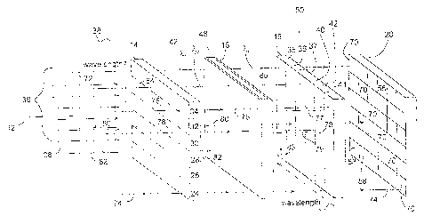
Referring now to Figure 2 and 3, major components of a spectrofluorometer 10
are shown. Optical
radiation traveling along an excitation light path 12 passes into a linear
variable spectral filter 14.
Spectral filter 14 is a device which has bandpass wavelength characteristics
which vary along its length.
More particularly, at the bottom of filter 14, one wavelength would be passed
in the region defined by the
dashed lines. In the next filter region above that filter region like having a
different wavelength will be
passed, perhaps a wavelength which is 5 nm longer. This sort of device is made
by advancing a mask
having the width of one of the regions illustrated in dashed lines in the
figure, from one discrete position to
another and applying a different multilayer structure at each position to give
the corresponding stripe of
bandpass material the desired optical bandpass characteristic.
The manufacture of such a filter is known in the art and forms no part of the
present invention. Such filters
may be purchased on the open market and are available from, for example,
Reynard Corporation under
their catalog No. 4610. Such a filter has a spectral range of 400 to 700 nm.
It is relatively small and
compact, being 60 mm long, 25 mm wide and 5 mm thick. A typical spectrum
length would be 44 mm,
with dispersion varying between .12 and .17 mm/nm.
The linear variable spectral filters sold by this corporation tend to vary in
their characteristics, with a
spectrum length varying form 37 to 51 mm. matching of the filters used in the
embodiment of Figure 2 is
desirable. Alternatively, a computer reading the output of the system may
calibrate the software against a
known source.
A sample receiver 16 is located between the first spectral filter 14 and a
second linear variable spectral
filter 18. Sample receiver 16 is a vessel which defines a volume for receiving
a sample which is to be
analyzed. It may be a rectangular solid made of glass, plastic or any suitable
material. It may also be as
simple as a glass slide with a smear of the sample, or even a solid film of
the sample material, such as
tissue, paper from a paper mill whose operation is being monitored, and so
forth.
Such a sample may be a solution derived from a material being tested, blood,
the output of an HPLC liquid
chromatography column, or the like. If the output of an HPLC column is being
monitored, the receiver 16
may have a liquid input port and a drain, and the dimensions of the receiver
would be such that capillary
-4-
CA 02392228 2002-05-15
WO 01/36948 PCT/US00/31775
action insures the presence of sample material throughout the excited regions
of receiver 16. A close-
coupled discharge (CCD) sensing element 20 measures the relative position and
intensity of light rays
traveling along a resultant light path 12. See Figure 3.
Sensing element 20 is preferably a CCD type of sensor although other types can
be used depending upon
the type of excitation light used and the sample to be tested. In Figures 3
and 5, detector 20 is shown as a
36 element matrix detector. The small number of elements or pixels is merely
for the convenience of
illustration and the illustration of the principles of the invention. In a
real device, the number of detectors
easily ranges into the hundreds of thousands of elements, and, depending upon
the performances desired
and the nature of the software reading out the signal from the detector, the
number of elements in detector
may range into the millions of pixels.
In principle, even film can be used in place of detector 20. An absorption
spectrum and lamp profile
(without sample) is shown as diagonal line 56 in Figure 5. In connection with
the preferred embodiment of
15 the invention, a suitable sensing element is the CCD sold by Instruments SA
on the Spectrum One. Each
of these elements are described in detail below.
Referring back to Figure 3, the borders defining the filter regions with
different spectral characteristics in
the first and second optical filters 14 and 18 are shown as dashed lines.
First filter 14 is a linear variable
20 spectral filter that changes its bandpass wavelength along the length or
planar axis 15 of the filter.
Wavelengths outside the desired transmission ranges are blocked by the
respective filter regions.
In a preferred embodiment, the spectral range from 400 to 700 nm is oriented
vertically, e.g., with shortest
wavelength filter region 24 at the bottom, then longer wavelength filter
region 26, still longer wavelength
filter region 28, a filter region 30 which passes a range of wavelengths
longer than those of filter region 28,
a filter region 32 which passes a range of wavelengths longer than those of
filter region 30, and the longest
wavelength bandpass filter region than 34 at the top. While the invention has
been implemented with a
spectral filter having the aforementioned wavelength characteristics, other
visible and non-visible bandpass
characteristics can be used depending on the nature and characteristics of the
sample to be tested.
The second optical filter 18 is substantially the same as the first optical
filter 14 except that it is oriented in
such a manner that its gradations are not
in line with those of first filter 14. The strips defining the bandpass filter
regions on filter 18 are preferably
at ninety degrees to those of filter 14. The advantages of this relationship
will now be described in
connection with the operation of the inventive system.
-S-
CA 02392228 2002-05-15
WO 01/36948 PCT/US00/31775
A light source 36 which may comprise a xenon lamp whose output is collimated
by a lens or reflector, or
any other suitable optical components produces an excitation white light ray
bundle 38, sometimes
referred to as illumination light, that travels along excitation light path 12
with a wide range of
wavelengths striking the surface of. filter 14. As white light ray bundle 38
passes through filter 14, selected
wavelengths are passed by each filter region, such that a wavelength
"gradient" from short to long
wavelengths is produced. This is referred to herein as a sample excitation
light 42.
As sample excitation light 42 passes through second filter 18, only those
wavelengths of light that are not
blocked pass completely through the filter 18. Since filter 18 is oriented at
a right angle to filter 14, most
of sample excitation light 42 is blocked. By way of example, ~,, passes
through filter 14 and filter 18,
while ~" passes through filter 14, but is blocked by filter 18. In this manner
a diagonal spectral line 56 is
transmitted onto sensing element 20. The theoretical center of this line it
illustrated in figure 5 by phantom
line 56. This intrinsic relationship between the two linear variable spectral
filters provides for simplicity
of design, ruggedness and compact size of the inventive spectrofluorometer 10.
Referring now to Figure 4, a sample receiver 16 is located between filter 14
and filter 18. Sample receiver
16 may be any of a number of conventional sample holding types or techniques.
As sample excitation light
passes through sample 44 some of the light energy is converted into
fluorescence emissions. The physics
of this conversion are well understood and generally involve the photon of
excitation radiation raising the
energy level of electrons in the excited atom to a higher energy level or
shell. When the electron snaps
back into its unexcited state, it emits a photon with an energy level lower
that the exciting photon, thus
resulting in the fluorescence having a wavelength longer than the excitation
wavelength.
Some of the sample excitation light is "absorbed" by sample 44 and does not
contribute to the emission.
The net result is to increase the kinetic energy of the atoms of the sample,
and thus raise the temperature of
the sample.
A resultant light ray bundle 50, exiting sample receiver 16, comprises light
rays which have exited filter 14
and fluoresence emissions from molecules that have been excited by light rays
which have exited filter 14.
Resultant light ray bundle 50 then passes into filter 18 where a selected
wavelengths of both spectral light
and fluorescent light are selectively blocked along the spectral gradient. The
portions of light ray bundle
50 passing through to sensing element 20 constitutes the absorption spectrum
52 of the material being
analyzed and appears along imaginary line 56 in Figure 5. This can be used to
identify sample 44.
As may be understood with reference to Figure 4, filters 14 and 18 are
substantially identical, but are
positioned with their bandpass filter strip filter regions 24-34 and 35-44
oriented at right angles to each
-6-
CA 02392228 2002-05-15
WO 01/36948 PCT/US00/31775
other. In accordance with the preferred embodiment of the invention, filter
region 24 has the same
bandpass characteristic as filter region 34. In accordance with the preferred
embodiment of the invention,
filter region 26 has the same bandpass characteristic as filter region 42.
Filter region 28 has the same
bandpass characteristic as filter region 40. Filter region 30 has the same
bandpass characteristic as filter
region 37. Filter region 32 has the same bandpass characteristic as filter
region 36. Filter region 34 has the
same bandpass characteristic as filter region 35.
Thus, the CCD elements 70, lying along line 56 in Figure 5, are the only
elements that will be illuminated
by the white light ray bundle 38 coming from the excitation source. Moreover,
because the fluorescence
spectrum constitutes only wavelengths longer than the excitation wavelength,
they will be blocked from
reaching elements 70 by filter I 8. Thus, only the absorption spectrum can be
seen along imaginary line 56
to provide a first identification of the sample.
Likewise, because the fluorescence spectrum constitutes only wavelengths
longer than the excitation
wavelength, these longer wavelengths will be passed by filter 18 to those
elements 58 of the CCD which lie
below line 56 in Figure 5. Thus, the elements 58 of the CCD which lie below
line 56 in Figure 5 produce
the fluorescence emission spectra of the sample under analysis. The resultant
fluorescence emission is
used to identify sample 44.
Referring back to Figure 4, the operation of the inventive system may be
better understood. In particular,
the output of the xenon lamp 36 constituting a broadband emission which is
collimated into white light ray
bundle 38 is caused to fall on filter 14, which outputs a plurality of stripes
of light energy at different
wavelengths. Because filters 14 and 18 are very thin, as is sample container
16, the output of filter 14 is
effectively "imaged" on the sample in sample receiver 16. The output of sample
container 16 is likewise
effectively "imaged" on filter 18. Finally, in turn, the output of filter 18
is effectively "imaged" on the
surface of CCD elements 58. The system works because all of the above thin
elements are in contact with
each other and CCD 20 to form the sandwich illustrated in Figure 2.
As noted above, light ray 72, which is one of the light rays in white light
bundle 38, because it is in the
bandpass range of filter region 34 on filter 14, and, naturally, in the
bandpass of optically identical filter
region 35, will pass through both filters and fall on CCD 20, if it is not
absorbed by the sample. The same
is true for light ray 74, which is in the bandpass of filter regions 24 and
44.
Light rays 76 and 78 will, on the other hand, be blocked by filter 18, after
being limited to the different
bandpass of facing filter regions of filter 14. Moreover, any fluorescence
emissions 77 and 79,
corresponding respectively to light rays 76 and 78 will also be blocked by
filter 18, as they must be longer
_7_
CA 02392228 2002-05-15
WO 01/36948 PCT/US00/31775
in wavelength than the bandpass of the filter region of filter 14 that they
pass through, and they fall on
filter regions of filter 18 that are formed by filter regions that have
shorter wavelength bandpass
characteristics.
In contrast, light ray 80 has a wavelength corresponding to filter region 28,
and thus more energy than light
passed by filter region 36. Thus, it is physically possible that the sample
will fluoresce with a lower energy
and correspondingly longer wavelength light ray 81 that will pass through
filter region 36 of filter 18.
Likewise, highest energy light ray 82 which passes through filter region 26
and the sample may emit a low
energy photon 83, which passes through filter region 35 and falls on the CCD
detector.
Conversely, it is physically impossible that a sample will fluoresce with a
higher energy and
correspondingly shorter wavelength. Thus, a photon of light energy 84 passing
through filter region 34 of
filter 18 has the lowest energy in the system and the sample cannot emit a
higher energy photon, and thus
any light 85, whether transmitted or emitted by the sample will be blocked by
filter region 38 which has a
shorter bandpass wavelength than filter region 34. Thus, any such light will
not reach the CCD detector.
Referring to Figure 6, it can be seen that line 56, in the case where filter
14 is identical to filter 18, is a
simple diagonal line. However, due to the nature of the manufacturing process
use to produce filters 14
and 18, the layout of the various bandpass filter regions varies rather
considerably. Accordingly, it is
necessary to accommodate such variations if one cannot go to the trouble of
trying to match identical filters
very carefully.
Such variations may cause line 56 to shift to the position illustrated by
reference number 56a in Figure 6.
Such variation occurs because the distance of oval which the series of
spectral filters is dispersed is greater
in filter 18 as compared to filter 14.
In the case of such variations, it is merely necessary to calibrate the
software to the pattern on CCD 20.
This can be done by determining the presence of the absorption spectrum and
then mathematically
adjusting the position of the fluorescence spectrum accordingly. This is done
on the basis that the opposite
ends of the absorption spectrum represent the horizontal and vertical limits
of the fluorescence spectrum.
Such determination can most easily be made without having a sample in the
inventive fluorescence
instrument 10.
As is alluded to above, filters 14 and 18 are made by depositing stripes of
material which form bandpass
filters on a substrate. As is also alluded to above, maximizing the thinness
of instrument 10 will also
maximize performance. More precisely, improved performance can be obtained by
minimizing the
_g_
CA 02392228 2002-05-15
WO 01/36948 PCT/US00/31775
distance between the active filter layer of filters 14 and 18 as well as
minimizing the distance between the
active layer of filter 18 and the sensitive face of detector 20. Thus,
exceedingly thin substrates may be
used to optimize the performance of the instrument.
Yet another approach is illustrated in Figure 7. In Figure 7 the convention of
labeling parts with identical
or analogous functions with numbers which vary by multiples of 100 has been
followed.
In Figure 7, the inventive spectrofluorometer 110 is excited by excitation
light 138 along path 112.
Excitation light 138 first falls on filter 114, causing it to pass through the
active layer 115 of filter 1 14 on
the far side of filter I 14. Light 138 then passes through the sample in
receiver or carrier 116. Light 138
then passes through the active layer 117 of filter 116. Active layers 1 I S
and 117 are formed on the
substrates of their respective filters. Such substrates may be glass, plastic
or any other suitable material.
After passing through active layer 117, light 138 passes through the substrate
of filter 116 and on to the
sensitive face of detector 120, from which it is sent to a computer or other
suitable device for interpreting
and displaying the output of the detector.
Yet another approach is shown in Figure 8. Here spectrofluorometer 220 is
excited by excitation light 238
along path 212. Excitation light 238 first falls on filter 214, causing it to
pass through the active layer 215
of filter 214 on the far side of filter 214. Light 238 then passes through the
sample in receiver or carrier
216. Light 238 then passes through the active filter layer 217, which is
disposed and manufactured onto
the output face of carrier or receiver 216. Alternatively, active filter layer
217 may be disposed on and
manufactured onto the input face of detector 220. After passing through active
layer 217, light 238 passes
onto the sensitive face of detector 220, from which it is sent to a computer
or other suitable device for
interpreting and displaying the output of the detector.
As will the apparent from Figure 8, the distance between filtered light
exiting the first active bandpass
layer in the inventive system 220, and the sensitive face of detector 220 is
minimized in Figure 8.
Accordingly, light which is not traveling perpendicular to the faces of the
filters, then, accordingly, is
dispersed in itself, travels over a minimized path length and, accordingly,
the dispersion is minimized, thus
eliminating the need for the focusing optics, which are so important in prior
art systems.
Referring to Figure 9, a spectrofluorometer 310 having the feature of being
able to block the excitation
wavelength of the system is illustrated. This is desirable because the
amplitude of the excitation
wavelength will often spread and overload the detector receiving light from
adjacent filter regions. The
instrument illustrated in Figure 9, operates in the same manner as the
instrument illustrated in Figure 4,
except for this additional feature.
-9-
CA 02392228 2002-05-15
WO 01/36948 PCT/US00/31775
In particular, it has a filter 314, a sample carrier 316, a filter 318, and a
detector 320. The characteristics of
all of these systems is the same as the instrument illustrated in Figure 4.
However, it also has a spectral
band reject filter 354, which is aligned, filter region by filter region, to
substantially identically opposite
filter 314.
More particularly, in accordance with the preferred embodiment of the
invention, filter region 323 has a
band reject characteristic with the same wavelength range as the wavelength
range of the bandpass
characteristic of filter region 324. In accordance with the preferred
embodiment of the invention, filter
region 325 has a band reject characteristic with the same wavelength range as
the wavelength range of the
bandpass characteristic of filter region 326. Filter region 327 has a band
reject characteristic with the same
wavelength range as the wavelength range of the bandpass characteristic of
filter region 328. Filter region
329 has a band reject characteristic with the same wavelength range as the
wavelength range of the
bandpass characteristic of filter region 330. Filter region 33 I has a band
reject characteristic with the same
wavelength range as the wavelength range of the bandpass characteristic of
filter region 332. Filter region
333 has a band reject characteristic with the same wavelength range as the
wavelength range of the
bandpass characteristic of filter region 334. The blocking of excitation
wavelengths is thus assured and the
detection of low amplitude fluorescence signals is enhanced.
Another embodiment, shown in Figure 10, is substantially identical to the
instrument of Figure 9, except
that active filter layer 415 of spectrofluorometer 410 is deposited on the
substrate of filter 414 on the side
of filter 414 closer to the sample to be analyzed, and active filter layers
417 and 455 are deposited on the
sensitive face of CCD 420 (on the side of filter 414 closer to the sample to
be analyzed). This is done in
order to minimize the lengths of paths of dispersion, and thus minimize
dispersion and optimize the
operation of the instrument. Active filter layer 455 is identical to filter
354 in Figure 9.
Active filter layer 415 is made by advancing a mask along the substrate of
filter 414 having the width of
one of the regions illustrated in the figure, from one region to the next and
applying the appropriate
multilayer structure at each position to give the desired stripe of bandpass
material the desired optical
bandpass characteristic. Active filter layer 417 is made by performing the
same process, first applying to
the sensitive face of CCD 420 the same series of different multilayer
structures at their respective positions
to give the corresponding stripes of filter layer 417 the desired optical
bandpass characteristic. CCD 420 is
then rotated in the plane of its sensitive face by 90 degrees.
Active filter layer 455 is made by advancing, along the rotated substrate of
CCD 420, a mask having the
width of one of the regions illustrated in Figure 10, from one region to the
next and applying the
appropriate multilayer structure at each position to give the desired stripe
of band reject material the
-10-
CA 02392228 2002-05-15
WO 01/36948 PCT/US00/31775
desired optical band reject characteristic. When the process is completed, the
result is a filter layer 455 is
the band reject analog of bandpass filter layer 415.
In accordance with the present invention, it is may be desirable, in order to
accommodate the insertion of
S different sample receivers or carriers 416, to vary the distance between
filter layers 415 and 417. This may
be achieved by mounting filter 414 on a horizontally moveable table 491 or
other mechanism. This enables
movement in the directions indicated by arrow 492.
The positions of layers 417 and 455 may be reversed by reversing their order
of deposit. Likewise, the
active filter layers may be deposited on the sample receiver or carrier to
provide sample carriers that have
filter patterns which may embody the operation of any of the systems described
above. Such sample
carriers may be specialized to optimize the analysis of certain classes of
analysis tasks, such as blood work,
where it may be desirable to perform special filtering, to block, transmit or
study certain portions of the
spectrum. One or more filter layers may be placed on either or both sides of
the sample carrier.
While an illustrative embodiment of the invention has been described, it is,
of course, understood that
various modifications of the invention may be made by those of ordinary skill
in the art without departing
from the spirit and scope of the invention which is limited and defined only
by the appended claims.