Note: Descriptions are shown in the official language in which they were submitted.
CA 02392378 2002-05-23
WO 01/39210 PCT/GB00/04494
X-ray Zoom Lens
The present invention relates to an X-ray optic and more particularly it
relates to an
optical arrangement which can focus electro-magnetic radiation in the range of
frequencies commonly referred to as X-ray.
Focussed X-rays are or have the potential to be used in a wide range of
applications such as X-ray lithography for the manufacture of micro-chips and
for
micro-machining, in spatially resolved X-ray fluorescence analysis, sub-
cellular
probing, X-ray microscopy and in scientific instrument manufacture. In these
applications an intense X-ray source is required and the ability to focus X-
rays can
increase the useable source intensity.
Known methods for producing focussed X-rays include the use of diffractive
optical components (zone plates) or multilayer mirrors. Although zone plates
are
capable of forming high-resolution images they, and multilayer mirrors, suffer
from
several drawbacks such as low efficiencies, the need for monochromatic
illumination
and small zone plate apertures.
Grazing incidence reflective optics are widely used in several applications
but
have not been used in high resolution imaging systems because of aberrations.
Systems which have been used mainly for hard X-ray applications are
Kirkpatrick-
Baez optics, Wolter optics, microcapillary optics, polycapillary optics and
micro
channel plate arrays.
-1-
CA 02392378 2002-05-23
WO 01/39210 PCT/GB00/04494
In polycapillary optics, which are described in articles by MA Kumakov 1998
Proc. SPIE 3444 pps. 424-429 and by HN Chapman, KA Nugent, SW Wikins 1991
Rev. Sci. Insrum. 62 1542-1561, a series of small (10-6m) curved channels are
used
and X-rays are transmitted down the channels and use grazing incidence
reflection to
focus the X-rays. Although polycapillary optics have large apertures, large
bandpass
and high transmission efficiency they are difficult to design and manufacture
as
several constraints have to be overcome, these include the limitation that the
channel
width, cross sectional shape and curvature are such that there are only a few
reflections down each channel (ideally two) as, with more than two
reflections,
correspondence between object and image conjugate points may be lost, so it is
necessary to vary channel width, shape and curvature along the length of the
channels. The open area of the channels at the optic entrance should be a
large
percentage of the total area (>80%), however a large open area makes the optic
very
fragile and variation in reflectivities, absorption and scattering due to
surface
roughness are disadvantages.
We have devised an X-ray optical system based on a microstructured optical
array (MOA) which overcomes many of the disadvantages of existing systems. In
addition, and most importantly, it can be used as an X-ray zoom lens, allowing
variable magnification and control of focal length
According to the invention there is provided an optical array which comprises
a plate, the surface of which is formed of a plurality of X-ray transparent
zones
separated by X-ray opaque bands, the X-ray opaque bands being of a thickness
such
that, when a beam of X-rays from a source is projected onto the plate, at
least some of
the X-rays are reflected off the outermost walls of the said bands and there
being a
control means able to shape the plate to form a curved surface so as to be
able to focus
X-rays passing through the plate.
-2-
CA 02392378 2002-05-23
WO 01/39210 PCT/GB00/04494
In an alternative aspect, there is provided an optical array comprising a
plurality of X-ray opaque bands separated by X-ray transparent zones, the X-
ray
opaque bands being dimensioned such that, when a beam of X-rays from a source
is
projected onto the array, at least some of the X-rays are reflected off walls
of the said
bands, the array being deformable to dynamically vary the angle of reflection
of said
X-rays.
There is also provided a method of focussing a beam of X-rays employing the
optical array of the present invention.
By thickness of the X-ray opaque bands is meant the distance measured from
the base of the bands to its top i.e. the height above the adjacent X-ray
transparent
zone.
The zones are preferably in the form of rings and that the structure comprises
a plurality of X-ray transparent channels separated by X-ray opaque walls. The
rings
on the plate can be in the form of concentric circles or they can be
elliptical, oval etc.
The walls preferably have a height such that there is at least one reflection
in
each channel and, in a thin flat plate, a small variation of angle of
incidence of the X-
ray on the outer wall of the channels can be used for one to one imaging, but
channel
diameters must be small to reduce losses due to unreflected X-rays, however if
the
channel diameters are too small some X-rays may undergo double reflections
from
both wall of the channels and be lost. If the plate is thicker aberrations can
be
induced as the incidence angle varies along the channel, but fewer X-rays pass
right
through.
The dimensions of the plate will depend on the application.
The width of the channels preferably increases radially outwards to allow for
the increasing incidence angle and preferably the width of the channels is
larger than
-3-
CA 02392378 2002-05-23
WO 01/39210 PCT/GB00/04494
the width of the X-ray opaque sections between the channels. The width of the
channels will depend on the application.
The plate can be formed by directly etching a substrate formed of an X-ray
opaque material so that the X-ray transparent channels are formed through the
plate,
or by depositing rings of X-ray opaque material onto a substrate in the form
of a plate
or membrane to build up the structure of the invention.
When the structure is built up on a plate or membrane a lost mould process
can be used. In this process a structure of the size and shape of the optical
array is
fabricated in a material which can be removed e.g. by melting, and a mould is
formed
from this structure and the material removed. This mould is then used to form
the
optical array of the invention.
Materials which can be used to form the array include metals such as nickel
and these can be supported on a substrate if required. The channel walls must
be
smooth to prevent loss of reflectivity. Typical roughness must be less than a
fraction
of a wavelength, which can be achieved for X-rays with electroplated nickel.
Other suitable material from which the plate can be made include silicon,
silicon carbide and the plate can be formed from a single silicon wafer of the
type
made commercially by Virginia semiconductors Inc. Such a silicon wafer can be
patterned to form the structure of the invention e.g. by isotropic plasma
etching,
lithography etc.
To focus the X-rays transmitted through the plate the plate is curved and the
greater the degree of curvature the shorter the focal length of the array. The
curvature
can be spherical, parabolic, etc. and the degree of curvature can be varied
depending
on the wavelength of the X-rays, the distance of the X-ray source from the
plate and
the purpose of the focussed beam of X-rays etc. The degree of curvature and
hence
-4-
CA 02392378 2002-05-23
WO 01/39210 PCT/GB00/04494
magnification achievable will be limited by the elasticity and stability of
the material
of the plate under bending stresses. The ability to vary the curvature enables
an X-ray
zoom lens to be obtained
The plate can be curved by any suitable method either before or after forming
the structure of the invention. For example, when the plate is made of
silicon, a
method of forming the curvature of the plate is to deposit a prestressed layer
on the
silicon wafer after it has been patterned to give a biomorph stress induced
curvature.
For example radial ribs of silicon are coated with a metal film which, when
cooled
will be in compressive stress. The degree of curvature and hence the focal
length of
the structure can be changed by varying the temperature at specific points by
localised heating e.g. using miniature heaters.
Another method of curving the plate is to apply a differential pressure across
the plate so that the plate is curved. For example the structure of the
invention is
formed on a silicon wafer by lithography the plate mounted in a sealed chamber
with
helium, which is X-ray transmissive, on one or both sides of the plate, by
varying the
differential pressure the degree of curvature can be varied.
An alternative method of curving the plate is to coat the plate with a
piezoelectric material so that variation in an electric current applied to the
piezoelectric material will vary the curvature of the plate.
The ability to vary the curvature, whichever method is used, enables an X-ray
zoom lens to be formed and X-rays can be focussed to provide a concentrated
beam
of X-rays with a controlled degree of concentration. This enables the MOAs of
the
present invention to give enhanced performance in existing or potential
applications
such as X-ray lithography, spatially resolved X-ray fluorescence analysis, sub-
cellular
probing, X-ray microscopy and in scientific instrument manufacture, imaging X-
ray
-5-
CA 02392378 2002-05-23
WO 01/39210 PCT/GB00/04494
microscopy, spatially resolved fluorescence microscopy, photemission
microscopy
and astronomy.
The present invention is not wavelength specific and can be used with hard
X-rays and soft X-rays of a range of wavelengths, including the range of
wavelengths
commonly referred to as Extreme Ultraviolet (EUV).
The invention is illustrated in the drawings in which:-
Fig. 1 is a schematic side view of a flat MOA
Fig. 2 is a schematic side view of a curved MOA
Fig. 3 is a front view of fig. 2
Fig. 4 is a front view showing the use of a biomorph and
Fig. 5 is a schematic view of the use of pressure to bend the MOA
In the drawings one reflection is shown although in practice there can be more
than one.
Refernng to fig. 1 a plate (1) formed from a silicon wafer has gaps (3) etched
on its
surface by isotropic plasma etching so as to form a series of concentric X-ray
opaque
bands of silicon (2) and X-ray transparent gaps (4). The gaps (3) are wider
than the
bands (2) to give an open web structure. In practice there will be many more
bands
than are illustrated. The plate can be fabricated by depositing bands (2) onto
a
substrate ( 1 ).
When X-rays from source A impinge on the plate (1) X-rays are reflected off
the inner surface of (2) to focus at B as shown.
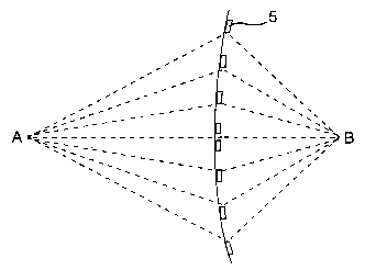
Refernng to fig. 2 the plate (5) is curved as shown so that the X-rays from
source A are focussed at (B) so that there is concentration of the X-rays.
-6-
CA 02392378 2002-05-23
WO 01/39210 PCT/GB00/04494
Refernng to fig. 4, in order to curve the plate (7) radial ribs (6) are formed
of
a metal such as nickel so that, as the metal cools, there is a biomorph
induced stress
which curves the plate (7) to form the shape shown in fig.2.
If the ribs are coated with a piezo electric material the curvature can be
electrically controlled by varying the current applied to the coating.
Alternatively the plate can be curved by localised heating.
Referring to fig. 5 a plate (8) is placed in a sealed pressure chamber (9) so
that
the two sections (9a) and (9b) are separated by the plate (8). The chamber is
sealed
by pressure sealing caps ( 10) and ( 11 ) and the sections (9a) and (9b)
contain helium.
By increasing the pressure PA in (9a) in relation to PB (9b) the plate (8) is
curved as
shown. One of the sections (9a) or (9b) can be exposed to atmospheric
pressure.
Each of the above enable the curvature to be varied and so the focus B of X-
rays from source A can be changed, allowing the plate to act as an X-ray zoom
lens.
shortened to increase the magnification.