Note: Descriptions are shown in the official language in which they were submitted.
CA 02392830 2002-05-29
WO 01/41929 PCT/CA00/01264
TITLE : DEVICE FOR BINDING A TARGET MOLECULE
CROSS REFERENCE DATA
This application claims convention priorities based upon provisional
application N° 60/168,767 dated December 6, 1999 and american patent
application N°
09/634,709 dated August 7'", 2000.
FIELD OF THE INVENTION
This invention relates multiple microchannels chip for biomolecule
imaging, and method of use thereof and in particular to providing a
microchannel chip
device which will be able to perform a large number of bio molecule tests
simultaneously,
as well as producing a uniform test environment for each biomolecule test and
eliminate
the statistical test to test variations.
BACKGROUND OF THE INVENTION
It is known in fluid dynamics that, due to the viscosity of the biological
sample containing fluid, which is usually water, the dynamic pressure to pass
this fluid
through and into the multiple channel glass panel increases as the
microchannel diameter
is reduced and the glass plate thickness increases. Threshold values are such
that, below
10 micrometers in channel diameter, increase in vacuum pressure is required to
force
water through the microchannels, and also structural integrity of the glass
sample then
becomes problematic. However, on the other side, by increasing channel
diameter beyond
10 microns and reducing the thickness of the glass plate, vacuum pressure is
still required
but to a lesser extent, while undesirable artifacts are generated in
particular increased
diffuse halos around the top access mouth of the channels. These undesirable
artifact
halos considerably deteriorate both the image quality and the sensitivity of
the test.
It is noted that fluid dynamics in a microchannel are not the same as those
in diametrally larger tubes, e.g. a water filled coffee mug. Indeed, because
of the larger
inner diameter of a coffee mug, when a water filled coffee mug is tilted from
an upright
condition to a laterally inclined position, the top surface menisk of the
volume of water
will not concurrently tilt and thus will remain parallel to the ground in both
instances,
although the longitudinal axis of the mug is no longer vertical in its tilted
condition. On
1
CA 02392830 2002-05-29
WO 01/41929 PCT/CA00/01264
the other end, due to surface tension properties and viscosity of the water
and due to the
micrometer grade diameter of the microscopic (micro-) channel, when a
microchannel is
tilted from an upright condition to a laterally inclined condition, the menisk
will not stay
parallel to the ground as it did in larger diameter cylinder such as a coffee
mug, and it will
tilt. With the tilted microchannel so that the perpendicular axis to the top
surface menisk
of the water volume inside the tilted microchannel will remain coaxial to the
longitudinal
axis of the tilted microchannel.
United States patent N° 5,843,767 issued on December 15' 1998 to
HOUSTON ADVANCED RESEARCH CENTER (inventor: Kenneth BEATTIE) -
hereinafter the " Beattie patent ", discloses a device for binding a target
molecule,
comprising a substrate having a multiplicity of discrete tubes extending
transversely
therethrough. These tubes extend orthogonally to the top surface of the
substrate. A first
binding reagent is immobilized on the walls of a first group of tubes, while a
second
binding reagent is immobilized on the walls of a second group of the tubes.
Such device is
for use in the identification or characterization of nucleic acid sequences
through nucleic
acid probe hybridization with samples containing an uncharacterized
polynucleic acid, e.g.
recombinant DNA, polymerase chain reaction fragments, etc... as well as other
biomolecules.
In the Beanie patent, these tubes are claims limited to a diameter ranging
between about 0.03 to 10 micrometers. The reason for the top threshold
diameter value is
that if your have upright tubes or channels as in Beanie, any diameter larger
than about 10
micrometers will enlarge optical halo artifacts at the top access mouth of the
tubes, and
accordingly, much reduced sensitivity .
During the 1990s, microfabrication technology has enables
miniaturization and automation of manufacturing processes in numerous
industries. The
impact of microfabrication technology in biomedical research can be seen in
the growing
presence of microprocessor controlled analytical instrumentation and robotics
in the
laboratory engaged in high throughput genome mapping and sequencing (see the
current
"Human Genome Project", with its first phase just completed). Optical
detection of
fluorescent labelled receptors is employed inter alia in detection for
sequencing.
2
CA 02392830 2002-05-29
WO 01/41929 PCT/CA00/01264
Detection can be achieved through use of a charge coupled device array, or
confocal laser
imaging technology such as DNA scope (TM).
Capillary tube glass arrays are already in use as high surface area
nanoporous support structures to tether DNA targets or probes for
hybridization. Such
capillary tube glass wafers contain a regular geometric array of parallel
holes or tubes as
small as 33 nanometers in diameter, or as large as several micrometers in
diameter. These
holes or tubes serve as sample wells for placement of a substantially
homogeneous
sample of a biomolecule within each hybridization site. The orifices are
fabricated using
excimer laser machining.
However, such prior art microscopic detection devices usually require
charged coupling devices, and cannot scan the full sample area. This is
because, as in the
Beanie patent, since you have vertical micro-channels, the diameter thereof
larger than 10
micrometers will produce much larger optical halo artifacts and will bring
about much
diminished microscopic sensitivity. This is why the claimed microchannel
diameter in the
Beattie patent is limited to a range from 0.03 to 10 micrometers.
Methods are also known in the art for delivering sub-nanoliter
microdroplets of fluids to a surface at submicron precision. A microjet system
or a
microspotter, capable of delivering subnanoliter DNA solution to the wafer
surface, can
thus be employed.
OBJECTS OF THE INVENTION
An important object of the present invention is therefore to improve upon
the above-noted prior art technology, in particular to that disclosed in the
Beanie patent,
supra, by providing a device which will be able to perform a large number of
bio molecule
tests simultaneously, as well as producing a uniform test environment for each
biomolecule test and eliminate the statistical test to test variations.
A further important object of the present invention is to use the capillary
tube as an environment that can produce an internal reflection known as
"pipping effect",
so as to increase sensitivity and resolution of biomolecule detection.
3
"tea .~ ' ~.. -,~;%~ » x~.
'~~ ~ '- ~ =~ ~ ~ ~QQ9724~~ ,~
t~ ~ ~, ~. a'»> a~ V V 3 .... H~ F~. ,'
- ... . :_ c, v
Still another ohject of the invention is to use the capillary tube ac an
cnvironmettt in which samples and rea~;cnls flow thmugh, to inc;rvasL the
interactions
bcawoun bionmlecuios so as to reduce tltc inauhation time and incrt;ase the
sensitivity atttl
resolution at th4 satnc lime;, to thus enable ustt of a more diluted sample
for the same
vllicicncy.
A beneral ohjeet of tha invention is tn r'educe labour costs and required
r:llectivc s:unl>le volume associated with operation ut'such dwices.
. ! 0 Summar~nf the invention
According to tha invention, then; is disclosed a rigid pane) chip for
supporting biological sarnrlca for observation with a microscope, said panel
chip defining
tt icrp flat surface, a bottom bearing surfacx, and at Bast a few channels
extending gena~aliy
parallel tcy arch uthrr from said top to bottom surfaex;s, each of said
channels defning a
I S top access mouth fcrr ingmsc of said biolot;ieal samples, and each said
channel having wh
an inner di.ntteter as to accommodata flow through viscosity of a bioiogicnl
samplo
containing lluid,
charactcrivcd in that each of said channel is obliquely inclined so as to make
an awtt;
an ~;I4 relative tv an axis pcrpt;ndicular to said top (tat surface.
2()
Prvferabty, the pant;! chip consists of either glass, quartz, po(ypropylcne,
pmlyolctin, nylon, or fitsed xilica. More: preferably, the panel chip will be
made troth
transparent gla,s. Must preferably, the Mass chip will have a thickncw ranging
between
(l.5 Ia 5 rnillirncters.
Prufcrably, said vhannels ar4 c:ylindroid. Preferably, said cylinttroid
c:hsinnrls haw a constant diameter rtngint; ltcetwuun IU to 2U00 micrometers,
rnort;
prcfurably, bvwu;n Si) to 200 microntctcrc, and most preferably, of about 100
m icrc >tn ~tvra.
3U
Said acute angle should rungc~ betwunn 20 to 80 degrees, and preferably
be ;:hcrut 42 del;rccs.
-4-
'_~~ CA 02392830 2002-05-29 AN9E~1DED S~-IEET
IPEAIEP
-n ,s,--emu o'r' , ~~. ~r~ ~~,.
~. ' ~ ° ~ U U J ~~: r~,.
Preti;rabiy, tttc number of said channels range between a few hundreds to
a few thauaands of said channels extending through the thickness c~f said
glues panel.
'i'he invention also relates to a method of observation by fiat surface laser
,tanner mf hiv.~lugic;al samples in a glass panel, the bless panel of the type
detining a top
flat surface, a bottom tx;uring surface, and a plurality of channels extending
generally
parallel to 4~;tclr other from raid top to bottorn surfac;ua and each defining
a tap access
mouth for the bialugical sample, the Cha11r1cIs being inclicted in an oblique
fashion so as to
make an acute; angle rc;lative to an axis perpendicular to the top flat
surtace of the glass
14 panel, and the ittnc;r diameter of each said channel being large enough as
to accamrntxlate
seduced vactnun assisted flow through viscosity of a biologi~dl sample
containing fluid;
th o nteth~xi including the. following steps:
a) providing tluorescein dyes inside the biological sample cantainittg
!laid;
IS
b) directing a coherent laser bc.~am transversely through a selected
channel tap access mouth and coaxially into the corresponding channel, se as
to excite the
fluuroscoin dyes, wherein an optically apparcrtt glow is generated by the
excited
tiuciresc;c;in dyes without a halo bv:ing generated about the top ac;eess
mouth;
2t>
c) allowing sufl'rcient time for the fluorescein dyes to projrrc;t the
optically rtpparent glow upwardly beyond said chanwl top access mouth; and
d) performing optical measurements of this fluoresccin glow
25 pruj~,c;tcd upwardly out of tttc; channel, to generate evidence data an the
chetttical
prc~pcrtics ttnd location of the biulugical samples.
'This invention also relates iv a method of observation by flat surface htscrr
scanner of biological samples in a glass panel, the glass panel of the type
defining a tap
' 30 flat srrrtitce , a bottom bearing surface , attd a plurality of channels
extcndittg generally
parallel tc~ each other from said tvp to bottom surfaces and each defining a
top aec~s
rnauth for the hinkyicai sample, the char~neis being inclined in an oblique
fashion so a.R to
snake a si~ui(icant acute angle relative to an axis perlx:ndicular to the tap
flat surfiflee of
-5-
f~~C~~~~ ~E"~~.t~ff
CA 02392830 2002-05-29 ~P~-/~~~~-='t'~J
CA 02392830 2002-05-29
WO 01/41929 PCT/CA00/01264
Figure 1 is a schematic perspective view of a prior art microscope and
computer system assembly, coupled to a CCD unit for observing a sample
supporting glass
plate;
Figure 2 is a schematic perspective view of a confocal imaging system for
surface inspection on a specimen holder of a microchip according to the
present invention;
Figure 3 is an enlarged partly broken isometric and sectional view of a
prior art microchip showing that the channels are orthogonal to the chip top
surface
Figure 3A is a top end view of two adjacent channels from the top chip
surface of figure 3;
Figure 4 is an enlarged partly broken isometric and sectional view of the
multiple channel glass plate of the invention, showing the slant of the
oblique channels
made through the thickness of the glass plate chip;
Figure 4A is a view similar to figure 3A but for the present invention chip,
and suggests that the observer has no direct line of sight between the top and
bottom ends
of each through micro-channel;
Figure 5 is a schematic view of a single straight prior art micro-channel
similar to those in figure 3, showing the light cannot enter the microchannel
entirely
without losing its power to reflection and also suggesting when the laser beam
is directed
perpendicular to the surface, it enters the micro-channel and exits from the
other end
without producing total internal reflection;
Figure 6 is a schematic view of another isolated prior art irregularly
shaped microchannel, suggesting how light can not enter entirely into the
channel without
having some being reflected, this nanoporous silicon with non uniform inner
wall showing
scattered internal reflection which contributes to an increase in cross-talk
and light
escaping from the micro-channels;
Figure 7 is a view similar to figures 5 and 6, but showing the preferred
embodiment of slanted channel inside the glass panel chip according to the
present
invention;
Figure 8 is a still larger scale sectional view of the slanted channel of
figure 7, suggesting how the various bio-molecules and proteins adhere to the
inside wall
of this slanted micro-channel tube of glass plate chip;
Figure 9 is a top end view of an alternate embodiment of circular chip of
the present invention;
6
CA 02392830 2002-05-29
WO 01/41929 PCT/CA00/01264
Figure 9A is an enlarged top end view of a central portion of the circular
chip of figure 9; and
Figure 9B is an elevational view of still another alternate embodimetn of
chip, having a conical shape with the channels disposed in an upwardly
radially inwardly
inclined peripheral fashion, for use in a centrifuge rather than with a vacuum
assist means
for the filling and drainage of the biological specimen liquid from the micro-
channels.
DETAILED DESCRIPTION OF THE PREFERRED EMBODIMENT OF THE
INVENTION.
Figures 3 and 5 of the drawings show prior art microchannels such as in
the Beattie patent, supra. Each such microchannel is a regularly array of the
unilength
type in perpendicular position to the surface of the plane. It is vertical or
upright, inside
the glass observation plate. This microchannel is of uniform length and shape,
and is
vertical. As further shown in figure 1, it needs to be scanned through the
entire length of
the channel for detection, it requires special scanning device, and is
therefore expensive. It
has average emission excitation, a cross-talk, and a halo circle around the
top sample
access end mouth constituting an artifact. It has average to low sensitivity.
Its maximum
operational diameter is 10 micrometers or less. It further needs seals and
vacuum pressure
to engage the water sample inside the microchannel, due to the microchannel
diameter
being too small for unassisted engagement.
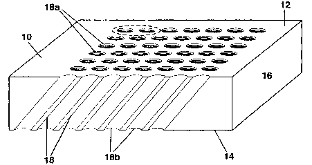
As is shown in prior art figure 3A, there is a top end view of two adjacent
channels when looking from top through the microchannels. Element 18a
represents the
top opening of the first channel, and element 18b represents the bottom
opening of the
same channels. Element 18 is the inner wall of the microchannels..
When one increases the diameter of the channels from 2 to 200
micrometers, i.e. by two orders of magnitude, the inner surface of the channel
will increse
by 200 divided by 2, i.e. by 100 times, by the surface area of the black hole.
In the prior
art system of figure 3A, the increase is of 10,000 times, i.e. by four orders
of magnitude.
This will therefore be a critical factor in deterioration of the image quality
which prevents
the inner diameter in the channel in figure 3A to be operatively more than
about 10
micrometers. This is shown in the following calculation in figure 3A:
7
CA 02392830 2002-05-29
WO 01/41929 PCT/CA00/01264
18b = 2 micrometers (channel diameter)
area of inner wall 18 Fig. 3A = 2 ~ x H, where H is the height
area of opening of each channel: 2/2 x 2/2 x ~ _ ~ (no unit used)
18b = 200 micrometers of channel diameter
area of inner wall 18 Fig. 3A : 200 ~c x H
area of opening of each channel = 200/2 x 200/2 x n = 10,000 ~ (no unit used)
We can see that a hundred time set increase in inner wall surface area 18
Fig. 3A, has resulted in 10,000 time (exponential) increase in black hole
artifact 18b Fig.
3A. But this is not the case in the present invention, as illustrated in
figure 4A, since there
is no black hole or halo artifact represented when the diameter of channels
increases from
2 to 200 micrometers. The black hole or halo artifact of the prior art 18b
Fig. 3A, where
there is lack of flurorescent glow, when it is viewed from top position and
this gives a dark
and halo like appearance in image capturing.
Moreover, inspection of light imaging in prior art figure 3A is performed
through tedious multiple scanning of transverse strata along the full length
of a chip
microchannel, contrary to the surface scan of the present invention at figure
4A.
Figure 2 alternately shows a confocal imaging system for use with the chip
of the present invention. System M includes a specimen holder N, for
supporting the
sample containing chip, a laser gun O for beaming light onto the specimen
holder, and a
black hole light detector P, for imaging the biomolecules inside the chip
channels. A
beam splitter Q and tilted mirror assembly R, is mounted intermediately of the
specimen
holder, light detector and laser gun. A pinhole member S is mounted between
the light
detector and beamsplitter. A laser scan lens T is mounted between the specimen
holder
and the scanning minors. A spatial filter and beam expander, U, is mounted
between the
laser gun and the beamsplitter.
In figure 2, the beamsplitter allows both free laser beam passage from gun
O to specimen holder N in a first direction, and return passage of the
biomolecule imaging
beam from the specimen holder to the detector P through reflection against
intermediate
8
CA 02392830 2002-05-29
WO 01/41929 PCT/CA00/01264
beam sputter Q. The light detector should be coupled to a suitable microscope,
for
example a microscope having parfocal arms and submicron diffraction limited
resolution
with 12 or 16 bit dynamic range detection, such as for example sold under the
MACROSCOPE or DNAscope trademarks by BIOMEDICAL PHOTOMETRICS inc.
(Waterloo, Canada).
Figure 6 of the drawings shows an alternate prior art microchannel. This
porous silicon nanochannel, which has a diameter of less than 1 micron, i.e.
about 0.03
micron, is an irregularly shaped array of variable length and size. It is of
non uniform size
and length. Its level of excitation emission is minimal. It has maximum cross-
talk.
Again, it has a small inner diameter of less than 1 micrometer, meaning once
again that for
engagement of sample fluid therein, high vacuum pressure is required, which
results in
compromising the structural integrity of the chip. Also, various sample fluid
quantity is
bounded due to varying length and non uniformity.
Figures 4 and 7 show a micro-chip 10 according to a preferred
embodiment of the present invention. The glass plate chip 10 defines top and
bottom flat
surfaces 12, 14, respectively, being parallel to one another, spaced by a full
thickness
glass body 16. The present invention micro-channel forms a regular array of
uniform
length micro-channel tubes and extends along a pre-established constant
angular
orientation. More particularly, the hollow microchannel 18 extends obliquely
relative to
an axis perpendicular to both top and bottom flat surfaces 12 and 14. The
bottom flat
surface 14 is the bearing surface of the glass plate. The top mouth 18a of the
microchannel 18 is coplanar to the top flat surface 12 of the glass plate,
while the bottom
mouth 18b of the microchannel 18 opens at the bottom flat surface 14 of the
glass plate.
The microchannel is of uniform throughout length, and provides an oblique
fluid flow
through. This microchannel can use CCD (charged coupling device), PMT
(photomultiplier tube) or flat surface laser scanners, for biological sample
detection. It has
maximum emission excitation. It has minimum cross-talk. Most importantly, no
artifact
halo circle is generated at the top mouth 18a, where observations are
performed preferably
by a flat surface laser scanner. The present invention microchannel has
maximal internal
reflection and maximal sensitivity features. It is a larger microchannel
diameter than the
prior art ones, bringing about less plumbing problems. Since detectors P are
placed on top
9
CA 02392830 2002-05-29
WO 01/41929 PCT/CA00/01264
of channels, the light which exits the channels are in vertical column and
parallel to each
other without having the blackhole in the center.
In the present invention microchannel, the obliqueness thereof relative to
the glass panel top surface, forms a fixed angular value being computed from
snell's law:
n1 sin 0 = n2 sin cp
with the refractive index of air being by definition 1, of water, 1.33, and of
glass, ranging
between 1.41 to 1.61 (with an average of 1.51) depending on the manufacturer.
As is known from college level physics, Snell's law is a law of geometric
optics, that defines the amount of bending that takes place when a light ray
strikes a
refractive boundary. Where n1 is the index of refraction of the medium in
which the
incident ray travels, 0 is the angle with respect to the normal at the
refractive boundary at
which the incident ray strikes the boundary, n2 is the index of refraction of
the medium in
which the refracted ray travels, and ~ is the angle with respect to the normal
at the
refractive boundary at which the refracted ray travels. If a ray travels from
a medium of
lower refractive index into a medium of higher refractive index, it is bent
toward the
normal. If it travels from a medium of higher refractive index to a medium of
lower index,
it is bent away from the normal. Total internal reflection occurs when light,
in a higher
refractive index medium, strikes an interface with a medium with a lower
refractive index,
at an angle of incidence (with respect to the normal) greater than the
critical angle. This
reflection occurs even in the absence of a metallic reflective coating (e.g.
aluminum or
silver).
This microchannel obliqueness critically enables the laser light beam to
penetrate the sample containing fluid inside the microchannel at its maximum
strength.
For calculating the oblique angle (3 of the microchannel, i.e. the angle
between the longitudinal axis of the microchannel and the axis perpendicular
to the top
surface of the glass panel into the thickness of which the microchannel is
nested, this is
based on the properties of the glass material and the refractive index:
CA 02392830 2002-05-29
WO 01/41929 PCT/CA00/01264
a+(3=90°-
(3+8= 90°-
13= 90- 8
The incident ray of the laser beam is perpendicular to the top surface of
the sample glass plate, so the laser beam penetrates to the maximum without
any
undesirable reflection; that is important since the stronger the beam, the
more fluorescein
dyes within the channel will be excited.
As suggested in figure 7 of the drawings on file, once the laser beam 20
hits the glass side wall of the channel tube, it produces both reflected beams
20' and
refracted beams 20". If angle 0 has a value of 90 degrees, it is parallel to
the side of the
glass core, and remains inside the channel tube. If on the other hand angle 8
has a value of
zero, then the light will exit the channel tube. The critical angle is chosen
where the
maximum internal reflection to occur and minimum light to escape from the tube
18. This
critical angle is important because if the angle is less than this value, some
light goes
through the chip glass core and escapes from the light channel tube 18. Let's
assume that
the critical angle for a glass material with refractive index of 1.46 is equal
to 44-°°. The
oblique angle (3 = a = 90 - 44 = 46. This oblique angle is set to produce the
maximum
total internal reflection and the minimum loss due to refracted beam.
Alternately, the chip could be made from non-transparent material. Then,
the microchannel 18' should be lined with an inner light reflecting coating
18a', preferably
made from a metallic material selected from the group comprising aluminum and
silver.
In this format, this alternate embodiment of chip 10' need not be transparent.
The channels
still remain in oblique flow shape but there is a reflective metallic coating
18a' (see figure
8). This metallic coating will usually be aluminum, having an average of 90%
reflectivity
between 200 and 1000 nanometers (nm). Also, vacuum deposited of several other
metals
makes excellent reflectors. The protective monolayer 22 in figure 8, shields
layer 18a'
from oxydation that can be a deposit of silicon (Si02) or magnesium fluoride
(MgF2) or
the other, to insure high reflectance from the UV to the infrared range. The
oblique flow
shape of the micro-channels help to ensure that the maximum level of light
penetrates and
exits from the microchannels. Since the inner channels are coated with
reflective material,
11
CA 02392830 2002-05-29
WO 01/41929 PCT/CA00/01264
the light does not escape to the core material and exit at its maximum.
Therefore, there is
no Snell's law or critical angle, but only an oblique angle.
We will now address the present invention oblique flow technology.
Although flow through chip known as the three dimensional chip has many
advantages
over the flat surface chip, there are nevertheless major inherited problems
with the nature
of these chips that make them highly undesirable and economically
unattractive. These
problems include:
- plumbing;
- detection; and
use of expensive microscopy and devices that can scan the length of the
channel, for
detection.
On the other hand, with oblique flow technology, there is a new class of
three-dimensional gene chip that has addressed these problems.
With the plumbing problem, the pressure required to pass liquid through
the top access mouth of the microchannel, increases as the microchannel
diameter is
reduced and the glass plate thickness is increased. More particularly, as the
prior art
microchannel inner diameter decreases below 10 ~ (micrometers), there is
required a
higher vacuum pressure level and it becomes problematic in maintaining
structural
integrity of the chip. On the other hand, by increasing the micro-channel
diameter and
reducing the glass plate chip thickness, undesirable artifacts are generated
including
diffuse optical halos around the top access mouth of the microchannel. This
halo artifact
will deteriorate the image quality of the laser surface scanner, hence the
lateral intensity
comparison of different micro-channels. Also, by reducing the channel diameter
and
increasing the number of channels, the structural integrity of the chip will
be
compromised.
Alternately, and as illustrated in figure 9B, the chip instead of being
rectangular (as in figure 4), may be conical or circular in shape. The array
of micro-
channels 18' would then be disposed in an upwardly, radially inwardly inclined
fashion.
With such an alternate chip 10', the power assist means for drainage and
filling of the
micro-channels 18' with the biological sample solution, instead of being small
vacuum
assisted means, can be replaced by a centrifuge. The centrifuge may operate
e.g. at 2500
12
CA 02392830 2002-05-29
WO 01/41929 PCT/CA00/01264
RPM for about 2 minutes, to allow the biological sample solution to engage and
settle
inside the micro-channels. It is noted that such centrifugal technique for
filling the chip
oblique microchannels with biological sample solution, would not be effective
in the prior
art chips having vertical (non-oblique) microchannels. Indeed, in the prior
art chips, the
liquid inside the microchannels cannot be drained off from the bottom,
contrarily to the
case with oblique angle micro-channels according to the present invention. The
spotting
of material on a conical chip is also easier than on a rectangular chip.
Imaging detection
can be less bulky, since the scanning could be facilitated by the circular
motion of circular
disk along its center. A hand held and portable device is achieved from
afforded size
reduction. These are critical differences compared with prior art techniques,
generating
unexpected results.
As for the detection problem, most prior art microarrays are produced on
microscope slide glass, where the binding reaction and signal generation
occurs within a
single plane. In the three-dimensional layout of gene chip, this binding
reaction occurs
through the thickness or depth of the chip. Therefore, depth of field becomes
more
important since the signal must be collected throughout the thickness of the
chip.
Conventional commercial microarray readers which use confocal scanning optics
are not
appropriate for these chips. Only expensive custom-built CCDs are large enough
to image
the entire microarray in a single detection step. Therefore, confocal concept
of acquiring
signal from a very thin optical slice, enters in conflict with three
dimensional geometry of
flow through chip. In order to produce a good lateral resolution to
distinguish the
individual spot, the light should be collected from the entire thickness of
the chip. There is
therefore a tradeoff in resolution between lateral and depth of field, and
this imposes extra
weight to the section criteria. The higher the DNA, the greater lateral and
depth resolution
is achieved. For example, the image area for 1 X objective is
8.5 x 6.8 mm
wherein for 40 X objective, it is reduced to;
0.22 X 0.17 mm.
The present invention oblique flow is much different. Indeed, the oblique
flow chip has addressed the above problems with a totally new design. As it is
shown in
figure 7 of the drawings, the light or incident ray must penetrate the
microchannel top end
mouth and excite the fluorescent molecules present inside the sample fluid ,
and emission
13
CA 02392830 2002-05-29
WO 01/41929 PCT/CA00/01264
light must be able to escape from within the tube. This is achieved at its
maximum
efficiency when the incident ray is perpendicular to the top free surface of
the chip, and
reflected ray is zero. In this scenario, all the light will penetrate the
tube. By choosing the
8 critical angle for maximum internal reflection and minimum loss of
refraction to the
chip core material, the oblique angle (3 can be computed . After the
fluorescent
molecules from within the channel tubes have been excited, most of the
emission light will
exit perpendicularly to the top chip surface, which will result in an improved
optical
collection and detection system, as is shown at 20 in figure 7.
In oblique flow:
a) there is no need to collect light from within the entire thickness of
the tube, since it can be collected from the top microchannel mouth surface
18a surface
and act as a flat surface chip. The need for expensive devices with special
objective lenses
is therefore eliminated.
b) the halo artifact which is seen in conventional three dimensional
chip, disappears. This will result in more uniformity and consistency in
imaging
intensities of various channel when the intensities comparison plays a crucial
role in
determination of end result. That is to say, as one looks e.g. through an
empty tube, the
bottom outer end of the tube will obviously disappear from view when the
viewer tilts the
tube.
c) By increasing the light penetration and emission and maximizing
total internal reflection and minimizing the cross-talk, which in turn will
increase the
detection sensitivity, the channel diameter is allowed to increase, thus
enabling decrease of
the problem associated with liquid passing through the channels and high
pressure
vacuum, which jeopardizes the chip structural integrity.
Since the refracted ray is minimized by choosing the right angle 8 or
critical angle, therefore the cross-talk is minimized.
The cross-talk is an important phenomenon in image analysis. Since most
of flat surface chips are scanned using a laser beam, the cross talk could be
minimized by
14
CA 02392830 2002-05-29
WO 01/41929 PCT/CA00/01264
directing the incident beam with the appropriate critical angle. This is more
noticeable
where the light should be travelling through the fiber optics for miles.
On the contrary, in prior art figure 6 for example, since the microchannel
has non-uniform internal space with different dimension through the length of
the chips,
the cross-talk reaches its maximum and most light will escape from the
channels.
Moreover, since the length of the microchannels vary and no two channels are
the same,
there is various quantity of fluorescein dye bounded to these channels; this
will in turn
result in various intensity due to uneven quantity of bound molecules.
Figure 8 schematically suggestes how the biomolecules in the sample
solution are bound to the inner wall of the cylindroid channel tube 18. Also
in figure 8,
element 18a' is an interface which has a lower refractive index than element
18. This layer
could also be made of reflective metallic coating, such as aluminum or silver
for the type
of channels with inner metallic coating. These biomolecules may include:
- antigens A, connecting antibodies B to the wall of channel tube 18;
- enzymes C, conjugated with specific antibodies B' to the antigens A' and
antibodies B combination;
- gold particles D, also conjugated with specific antibody B;
- DNA molecules E, connecting fluorescein molecules in their excited
fluorescent
state, F', to the inner wall of channel tube 18, or connecting a secondary
antibody
B being conjugated with a specific enzyme to the inner wall of channel tube
18.
- Substrate F is required for colour formation of enzyme C conjugated antibody
B'.
It is noted that the issues of critical angle and preferred angle is relevant
to
the transparent chip embodiment, but not to the chip with reflecting metallic
inner coating
of the micro-channels. In the latter chip embodiment, once the light enters
the micro-
channels, it does not have a chance to escape because of metallic coating. The
general
concept of the metallic coated microchannel chip is that this reflecting inner
coating on the
inner wall of channels, once a particle or gold tagged biomolecule is used for
detection, it
become tarnished so that there appears an opaque or black layer on this
reflecting coating
surface and light can not pass through efficiently therefore, the reduction in
light intensity
reflection within the channel will determine the property of the biomolecule;
it is also a
CA 02392830 2002-05-29
WO 01/41929 PCT/CA00/01264
cheaper and easier to implement technique. Where we have gold tagged
biomolecules, the
silver enhancement technique always follows, so as to increase the entensity
of the gold
technique. In the transparent chip concept on the other end, the fluorescent
dye produces
when excited more light and alerts that there is a positive result.
16