Note: Descriptions are shown in the official language in which they were submitted.
CA 02393577 2002-06-03
WO 01/42939 PCT/US99/29627
DESCRIPTION
MEASUREMENT MODULE AND SYSTEM FOR MONITORING THE
STATUS OF ARMORED VEHICLE ELECTRONIC COMPONENTS
Technical Field
The present invention relates generally to measurement appliances and
diagnostic testing equipment. More specifically, the present invention relates
to data
measurement devices and in particular to digital measurement collection
devices.
Background Art
Military armored vehicles have increased greatly in complexity over the last
50
years. Tanks in particular have undergone radical improvements over that
period and
1 o today bristle with internal electronics. Internal electronics of the
modern tank not only
augment offensive capabilities, but also now support primary power systems,
such as
propulsion and power transmission. The augmentation of internal tank systems
with
electronics allows for precise monitoring of maintenance schedules and the
recording
of historical performance of subsystems for later maintenance analysis. 1n
turn,
improved monitoring procedures based upon augmented internal electronics has
led to
overall operational readiness of our tank forces.
Increased complexity of internal electronics for modern armored vehicles has
led
to a new complexities and in particular has led to difficulty in monitoring
internal
failures in vehicle component electronics or Line Replaceable Units ("LRUs")
as they
2o are commonly referred to.
In the past and currently with some vehicles such as the M 1 A 1, tank fault
isolation consisted of"fix-on-failure" response or repair through manual fault
isolation
procedures, typically with the assistance of detailed technical manuals. The
former is
unacceptable since a critical failure in an electronic component in the field
can have
disastrous effects on a tank command's readiness. The latter, on the other
hand, requires
cumbersome test equipment, including testing interface boxes, specialized
cables, and
adapters, and an array of technical manuals. Much of which is difficult or
impossible
to apply in field operations. The test set currently being used for the M 1 is
the
Simplified Test Equipment - M 1 Series Vehicle and M2/M3 Fighting Vehicle
Systems,
or STE-Ml/FVS for short. A high level of experience and expertise is required
by an
operator of STE-M1/FVS test equipment.
CA 02393577 2002-06-03
WO 01/42939 PCT/US99/29627
In response, some newer tanks have features that assist in fault isolation
procedures. For example, .he Bradley Fighting Vehicle has a system 1553 data
bus
which may be used to run >=wilt-In-Test ("BIT"). A run-time BIT allows for
isolation
to a specific ambiguity group., but additional test equipment must be utilized
to break
the ambiguity to a specific LRU. Moreover, even with the advent of a data bus
that
supports testing, all current fault isolation testing must be performed in a
non
operational maintenance mode, and testing equipment must still be carried to
the vehicle
with the associated removal of installed operational cables to each LRU in
favor of the
testing cables. Therefore, fault isolation of LRUs in current armored vehicles
is difficult
and limited in availability.
Therefore, there exists a need in our current fleet of military armored
vehicles,
such as tanks, for an apparatus that will allow for measuring performance and
evaluating
the status of LRUs while still in full operational combat mode.
Disclosure of Invention
The invention consists of a measurement module having one or more circuit
assembly boards, two data/power connectors, and a target connector to access
target
signals. The circuit assembly boards include electronics for accessing and
storing
selected signal data emanating from the connected target system. Signal data
may be
accessed from 1-128 target signal sources and sampled through two separate
channels.
An on-board microcontroller controls signal selection and data sampling rates
and also
provides recorded data transfer over a USB bus to a host computing device. The
host
computing device has the capability of running a testing application for
sending
commands to each measurement module to retrieve target signal data from the
module's
buffer memory. Using proper testing application functions from the host
computing
device, each module can be commanded to access and store representative data
from a
number of signal sources at each target system. Each module can be connected
to
another module, and to the host computing device over the USB. The host
computer
device may be detachably connected to the USB, and there-through to the
modules, at
will. Power is provided via the interconnecting cables to each module.
3o The invention solves the need in the industry to provide a method,
apparatus, and
system for testing an armored (or any type of) vehicle in a stationary testing
mode or
while in full and continuous operation. The invention provides an economical
solution
2
CA 02393577 2002-06-03
WO 01/42939 PCT/US99/29627
to tank fault isolation at a significantly reduced expense and significantly
reduced labor
expertise.
Other features and objects and advantages of the present invention will become
apparent from a reading of the following description as well as a study of the
appended
drawings.
Brief Description Of Drawings
A measurement module and system incorporating the features of the invention
are depicted in the attached drawings which form a portion of the disclosure
and
wherein:
to Figure 1 is an exploded perspective view of the measurement module;
Figure 2 is a perspective view of an alternate embodiment of the measurement
module;
Figure 3 is a system component schematic of the electronics of the measurement
module;
~ 5 Figure 4A is combined perspective and diagrammatic illustration of the
relationship between the measurement module, an associated target system, and
the
connecting USB bus;
Figure 4B is diagrammatic illustration of the measurement system installed in
an armored vehicle;
20 Figure 5 is a system flowchart showing the top level processing steps of
the
measurement module anticipating a testing command from the host computing
device;
Figure 6 is a system flowchart showing the processing steps taken by the
measurement module in responding to a measurement command from the host
computing device;
25 Figure 7 is a system flowchart showing the processing steps taken by the
measurement module to transmit data to the host computing device;
Figure 8 is a system flowchart showing the processing steps taken by the
measurement module as a hub device in communicating with the host computing
device;
and,
30 Figure 9 is a system flowchart showing the processing steps taken by the
measurement module as a proprietary function device in communicating with the
host
computing device.
3
CA 02393577 2002-06-03
WO 01/42939 PCT/US99/29627
Best Modes for Carrying Out the Invention
Referring to the drawings for a better understanding of the function and
structure
of the invention, it will be shown that generally the invention comprises a
series of
measurement modules interconnected via a high-speed USB bus and connected to a
host
computing device. The measurement modules are assigned and electrically
connected
to preselected LRU target component sub-systems of an armored vehicle, such as
a tank.
The LRUs can be anything from complex communications and target identification
sub-
systems to simple power transmission RPM shaft encoders. Measurement modules
can
be mounted directly to or inside an existing LRU, or can be fully integrated
into the
electronics of an LRU. A host computing device, such as an on-board controller
or a
connected notebook computer having the necessary USB drivers, controls the
access and
assimilation of data from each target system through the measurement modules.
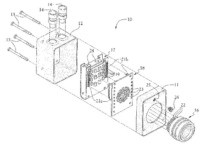
Referring to Fig. 1 for a better understanding of the measurement module, it
may
be seen that the module 10 includes a two piece housing having a top portion
11 and a
bottom portion 12. Screws 13 secure the top and bottom portions together that
hold the
internal electronics. The housing pieces are made of material suitable for the
module
and internal components to meet military specifications such as temperatures
ranging
from -40°C to +85°/C while in operation and -55°C to
+125°C for storage. Two
data/power connectors 14 extend from the upper side of the module for
connection to
the upstream and downstream paths of the USB. A connector 16 electrically
connects
the module to an assigned target system.
Housed within the module 10 are electronics for capturing target system data.
Two circuit card assemblies 17, 18 hold a series of integrated circuits 19
that implement
the functions of the module. Circuit card assembly 17 comprises a folded rigid-
flex
mufti-layered composite board onto which integrated circuits 19 are soldered.
Assembly
18 is a conventional mufti-layered plastic substrate also holding soldered
components.
Both boards have circuits soldered to both sides. Assemblies 17 and 18 are
connected
together through header connectors 21 a,b and through which they communicate.
Assembly 18 includes a series of resisters and diodes to provide for
electrical isolation
of target system inputs to protect against surges that may damage integrated
circuits on
assemblies 17 and 18.
4
CA 02393577 2002-06-03
WO 01/42939 PCT/US99/29627
As may be seen, connector 16 has a series of solder contacts 22 that mate with
contacts 23 to provide 128 potential electrical signal sources to the module
electronics.
The data/power connectors 14 are soldered onto solder pads 24 to connect
directly to the
module integrated circuit electronics 19. An access port 25 is provided to
allow the
introduction of potting compound into the interior of the module and a set
screw 26 is
applied to seal the port after the potting process. Internal application of
potting
compound allows for a more rigid and environmentally sealed module.
Assemblies 17, 18, the connectors 14, 16, and housing portions I I , 12
combine
into a solid, unitary assembly through strategic use of internally positioned
flanges and
penetrating housing screw holes as shown. Flanges on connectors 14 and 16 in
combination with appropriate "O" rings create a sealed unit allowing the
module to meet
stringent military specifications.
Referring to Fig. 2, module 10 can be configured with alternate positioning of
the connectors as shown to facilitate alternate LRU compatibility. Also, this
embodiment simplifies the electronics of the measurement module 10 by allowing
direct
soldering of all connectors to the circuit assemblies in a static orthogonal
relationship.
Multiple circuit assemblies can be stacked on top of one another. Stacking of
multiple
composite circuit assemblies can also be accomplished using a single folded,
rigid-flex
assembly.
Referring now to Fig. 3, each measurement module 10 includes several
integrated circuits that comprise the module electronics. A microcontroller 31
controls
the module electronics in response to commands sent from a host computing
device and
also controls communications via a high speed USB bus. Commands and data are
transceived via upstream 32 and downstream 33 ports. The general duties of the
microcontroller encompass controlling the module electronics to receive
commands
from a host computing device and configuring other module electronics in
response
thereto, and to upload stored data from a target system to the host computing
device
upon request. A suitable microcontroller for the present invention is an Intel
80930
which has built-in input/output (I/O) support for USB, and which may access
both
internal and external program instructions.
Connection to a target LRU is achieved through a 128 pin connector 34 mating
into connector 16. Connector 16 is then soldered onto circuit card assembly 18
which
5
CA 02393577 2002-06-03
WO 01/42939 PCT/US99/29627
holds a series of resistive lo-ids 36 customized to match the electrical
conditions of the
target system. An array of ~ nodes and other line conditioning circuitry 37
protects the
module's internal electrical components from damage caused by voltage spikes
and
general ESD attacks. Exempl. ry products used in the line conditioning
circuitry are a
switching diode array part number MMAD 1103 manufactured by Microsemi and TVS
diodes P/Ns SM05-36 manufactured by Semtech Corporation.
Twin multiplexers 38 and 39 provide for 16 to I and 8 to 1 channel selection,
respectfully, thereby allowing for selection of up to 128 different signal
sources from
the 128 pin test connector 16. Analog devices makes analog multiplexers having
a part
1o numbers AD426 and ADG428 that satisfy the functional requirement of 38 and
39,
respectively. Source selection through 38 and 39 is achieved through 16 bit
bus
addressing 41 and control lines 42.
Analog to digital converter (A/D) 43 provides sampling and conversion of up to
two selected source signals into digital data for storage in static ram buffer
(SRAM) 46.
A/D 43 outputs data over a I 2 bit data bus 48. A/D 43 includes dual channels
A/B from
which simultaneous sampling may occur. Amplifier circuitry 44 further
conditions a
selected source signal into the A/D 43. Suitable industry parts for 43 and 44
are Analog
Devices AD7862 and instrumentation amplifier AD622, respectively. Control
lines 49
allow sampling control over various parameters such as conversion rate,
reference signal
input, and channel selection.
Field programmable (gate) array 52 includes glue logic and logical state
machines for control over A/D 43, SRAM 46, and Flash Programmable Memory 47.
FPGA 52 communicates with microcontroller 31 over two 8 bit buses that allow
for a
16 bit address path 53 as well as 4 additional control lines 54. Control lines
51 and 55
allow for the distribution of control signals to the SRAM and Flash Memory 47.
A
suitable SRAM for the module electronics is a Cypress Semiconductor CY62256
32K
x 8 static ram, and Atmel makes a suitable Flash programable 256K (32k x 8)
memory
AT29C256. The FPGA may be any one of a variety of field programmable arrays
suitable for the herein described functions.
3o Flash Programmable Memory 47 contains the firmware for control of the
microcontroller 31. Instructions are written and saved in the firmware memory
47 to
control the operation of the module 10 at the time of manufacture.
Microcontroller 31
6
CA 02393577 2002-06-03
WO 01/42939 PCT/US99/29627
accesses firmware instructions over bus 41 through FPGA 52. Since the AT29C256
is
erasable, any module 10 may be updated and upgraded to accommodate a new
firmware
store on demand.
As shown in Fig. 4A, a measurement module 10 is connected to a target
component system or LRU 56 via a connector 16-34. Up to 128 signals are
connected
to selected signal sources into the target system and routed back to the
module
connection. The positioning of the module relative to the target system can be
accomplished in a number of ways. The module can be remotely located and
connector
34 can provide access to selected signal sources. The module can be positioned
directly
on the target component system 56 and connected via 16 directly to a pre-
existing test
connector on the LRU. Or, the module electronics can be fully integrated into
the LRU
with only the upstream 32 and downstream 33 connectors exposed.
As may be more easily seen in Fig. 4B, various target component systems in a
tank 57 may be selected for analysis. Individual modules 10 are connected to
various
selected LRUs (1-6) and are connected to one another via data/power cables to
create
a testing network 58. The electrical function of the bus is a modified USB
configuration
with 4 power conductors and 2 signal conductors. The physical construct of the
cable
for the instant invention is more robust than a standard USB shielded cable in
favor of
a double shielded conduit assembly having an outer jacket, a type 1 EMF
shield, and an
inner liner (e.g. MIL-T-81914/2), and a central core of six conductors. The
power for
each individual measurement module 10 is supplied from an external power
supply via
the 4 power conductors of the measurement interconnect cables 60. The power
supply
source exists at the host computing point of either 59 or 61, and provides
+BVDC,
+15VDC, -15VDC, and Ground. Each upstream connector 32 of each module is
connected to a downstream connector 33 of an adjacent LRU except for a
terminating
system with each connector including a dust cover. For example, LRU 1
terminates the
testing network 58, but is connected via its upstream connector 34 to the
downstream
connector 32 of LRU 2. LRU 2 is in turn connected to LRU 3 via its upstream
connector, and so on. LRUs 1-6 combine over the USB to form a full testing
lattice.
A host computing device accesses and analyzes data via the individual modules
10. The host computing device can take the form of an onboard printed circuit
wire
board 59 to take advantage of other input/output devices that may be available
within
7
CA 02393577 2002-06-03
WO 01/42939 PCT/US99129627
a tank's 57 system, or it may take the form of a separate notebook computer 61
that has
connected access to the modules via the USB via a temporary access port 62. In
either
case, the host computing device and complementary power supply provide power
and
data command instructions to each of the modules 10 attached to each of the
target
systems 1-6, and must have sufficient processing power to run a testing
application and
interface with the USB.
Since command instructions from a host computing device are required to
activate a module into a data collection mode, real-time operational analysis
of target
LRUs would necessitate either the permanent installation of a host computing
board, or
l0 the bringing onboard of a notebook computer with the vehicle. Due to the
structure of
USB, any module connected to a LRU may be connected and disconnected from the
testing network at any time. Generally, any module is hot-swappable to the
testing
network 58 at any selected moment. Hence, new LRUs in a tank's system may be
connected at will by simply wiring a module into the LRU to access the
selected source
I S signals of the LRU. This feature allows for inclusion of all LRUs in a
tank system over
an extended time period to allow for the upgrading of LRUs having desirable
testing
points. Obviously, a USB electrical connection must be maintained to each
module.
Referring now to Figs. 5-9, it is important to realize pertinent capabilities
and
features of USB for a proper understanding of the invention. A complete
description
20 of USB is not necessary for a complete understanding of the invention,
however some
understanding of the underlying USB communication architecture is necessary to
understand the structure of the invention's communications protocols. The
present
invention implements USB version 1.1 (9-28-98), and the complete USB version
1.1 is
readily accessible over the Internet at the USB consortium web page
www.usb.org. The
25 specification 1.1 is hereby incorporated by reference and specification
terminology and
concepts shall be readily recited from version 1.1 hereafter.
The USB physical interconnection is a tiered star topology. A hub is at the
center of each star, and each wired segment is a point-to-point connection
between a
host and a hub or function, or a hub connected to another hub or function. All
USB
30 devices are either a host, a hub, a function, or a compound device. A
compound device
appears to other devices on the USB as a hub with one or more non-removable
USB
8
CA 02393577 2002-06-03
WO 01/42939 PCT/US99/29627
devices. The measurement module 10 in our testing system acts as such a
compound
device.
The USB allows devices to be added and removed during full operation of the
bus. All USB devices attach to the USB through ports on specialized USB
devices
known as hubs. Hubs have status indicators that indicate the attachment or
removal of
a USB device on one of its ports. The host queries the hub to retrieve these
indicators.
In the case of an attachment, the host enables the port and addresses the USB
device
through the device's control pipe at the default address. The host then
assigns a unique
USB address to the device and then determines if the newly attached USB device
is a
hub or a function. The host then establishes its end of the control pipe for
the USB
device using the assigned USB address and endpoint number zero. If the
attached USB
device is a hub and USB devices are attached to its ports, then the above
procedure is
followed for each of the attached USB devices. If the attached USB device is a
function, then attachment notifications will be handled by host software that
is
appropriate for the function.
Attachment of a new device to the USB initiates a bus enumeration sequence.
Enumeration allows each device to be identified and assigned a unique address.
Because the USB specification allows for attachment or detachment from the bus
at any
time, bus enumeration is an on-going activity for USB system software.
USB supports functional data and control exchange between the USB host and
a USB device as a set of either uni-direction or bi-directional pipes. USB
data transfers
take place between host software and a particular endpoint on a USB device.
These
associations between the host software and the USB device endpoint are called
pipes.
The USB architecture utilizes four basic types of data transfers: control
transfers; bulk
data transfers; interrupt data transfers; and isochronous data transfers.
Each measurement module 10 of the present invention contains a hub, an
internal function, and one downstream port for connection to other modules.
Upon
connection of a module to the host computing device, such as 59 or 6I, the hub
and
internal function proceed through the USB enumeration process that configures
and
assigns an address to the module, thereby preparing it for communication over
the USB.
The enumeration process typically takes 1 to 2 seconds, and thereafter the
module is
ready to accept commands from the host computing device (hereinafter "host").
As
9
CA 02393577 2002-06-03
WO 01/42939 PCT/US99/29627
additional modules are attached to the USB each shall go through the same
enumeration
process such that each is as: igned a unique address on the bus.
After enumeration, each module establishes specific endpoints at the hub and
function device levels. Each ~mb includes two endpoints and each function
contains
three endpoints through which the host computing device communicates. For each
module in the present invention, the hub and function endpoint configurations
appear
as follows:
Table 1.0 Endpoint
Assignments
Hub Endpoint 0 Control (setup tokens)
Hub Endpoint 1 Interrupt (port change info.
only)
Function Endpoint Control (setup tokens)
0
Function Endpoint Bulk Transmit (i.e. Function
I to Host)
single-packet mode
Function Endpoint Bulk receive (i.e. Host to
2 Function)
single-packet mode
The control and interrupt endpoints are used during enumeration and at any
time
at which a configuration change is detected by the host computing device. The
two
endpoints with which a host's testing application shall access a module's
functions are
endpoints 1 and 2, which are uni-directional pipes. A host application sends
commands
2o to the module via function endpoint 2, and data is received back via
function endpoint
1. For clarity, transmit (tx) and receive (rx) are shown in the above table
from a
module's reference point. To be consistent with the USB specification 1.1,
function
endpoint 2 is labeled the Write Pipe, and function endpoint I is labeled the
Read Pipe.
Prior to the host recognizing a newly attached module on the bus, an
information
file must be loaded into memory on the host. Upon connection of a new module
on the
USB, the host recognizes the existence on the bus of a new device and asks the
user for
an appropriate driver. The file USB.inf already present on the host is
accessed and
utilized as the correct interface driver for the hub portion of the module,
and the file
SIDECAR.inf present on the host shall be accessed and utilized as the
interface driver
CA 02393577 2002-06-03
WO 01/42939 PCT/US99/29627
for the function portion of the module. USB enumeration shall then proceed for
the new
module. Each of these files is a standard driver written to enable the host to
communicate with the modules over the USB.
After enumeration, the module is prepared to respond to four basic host
commands:
Table 2.0 Host Commands
Command Action Translation
to Single List MeasurementMeasure a single selected
source signal
once.
Dual List MeasurementMeasure two selected source
signals
simultaneously once.
Single Waveform Measure a single selected
source signal
continuously for XX XX cycles.
Dual Waveform Measure two selected sources
signals
continuously for XX XX cycles.
Each of the above commands is transmitted over the Write Pipe, and any module
response shall be sent via the Read Pipe. These commands must be correctly
embedded
within a valid USB bulk transaction with actual command residing in the Data
Phase.
For the Write Pipe, a valid bulk transaction would consist of an OUT Token,
then data,
then a handshake signal. For the Read Pipe, a valid bulk transaction would
consist of
an IN Token, then data, then a handshake. Further explanation of USB
transactions,
phases, and packet structure may be found in USB specification 1.1 already
referenced.
Two firmware embodiments for the measurement module 10 exist that
implement two slightly different sets of host commands. The first embodiment
utilizes
the data stream shown below for each host instruction:
CA 02393577 2002-06-03
WO 01/42939 PCT/US99/29627
Table 3.0 Command
Set (Embodiment
One)
Command Resultant Data Stream
(host->function, Hexadecimal
Values)
Single List Measurement02 HI LO
Dual List Measurement82 HI LO HI LO
Single Waveform 03 XX XX HI LO
Dual Waveform 83 XX XX HI LO HI LO
Legend: HI = A target signal number.
LO = A reference signal number.
XX XX = a 16 bit cycle count (number of measurements
performed in hexadecimal).
~ 5 The data phase of embodiment one for a bulk transaction returned to the
host via
the Read Pipe will depend on the particular command sent. Upon receipt of a
command
by a module, analog to digital sampling occurs continuously in A/D 43 until
sampled
data stored in the SRAM 46 is ready to be transmitted back to the host. The
maximum
data packet size that a module 10 can transmit back to the host is 8 bytes.
For sampling
2o data greater than 8 bytes, a module simply sends multiple 8 byte data
packets until all
sampling data present in the SRAM 46 associated with a particular command
sequence
has been transmitted to the host. Measurement values taken by a module are
represented as hexadecimal voltages. Table 4.0 below shows a listing of
expectant data
returns from each function to host for each host command:
12
CA 02393577 2002-06-03
WO 01/42939 PCT/US99/29627
Table 4.0 Expectant
Return Data by Command
(Embodiment One)
Command Resultant Data Stream
(function->host, Hexadecimal
Values)
Single List Measurement2 bytes sampled data
Dual List Measurement4 bytes sampled data
Single Waveform 2 x (XX XX) bytes sampled
data
Dual Waveform 4 x (XX XX) bytes sampled
data
Embodiment two of the command set allows for controlled waveform sampling
rates by allowing for the insertion of read time delays through
microcontroller 31
intervention. The resultant command set and resultant data streams appear
below in
tables 5.0 and 6.0:
Table 5.0 Command
Set (Embodiment
Two)
Command Resultant Data Stream
(host->function, Hexadecimal
Values)
Single List Measurement02 HI LO
Dual List Measurement82 HI LO HI LO HI LO
Single Waveform 03 XX XX HI LO
(Fast)
Dual Waveform (Fast)83 XX XX HI LO HI LO
Single Waveform 43 XX XX TT HI LO HI LO
(Slow)
Dual Waveform (Slow)C3 XX XX TT HI LO HI LO
13
CA 02393577 2002-06-03
WO 01/42939 PCT/US99/29627
Legend: HI = . ~ target signal number.
LO = A reference signal number.
XX ?:X - A 16 bit cycle count (number of measurement
performed in hexadecimal).
TT = Delay time between samplings.
Fast = Samplings are performed continuously without delay
insertions.
Slow = Samplings are performed continuously with delay
1 o insertions.
Table 6.0 Expectant
Return Data by Command
(Embodiment Two)
Command Resultant Data Stream
(function->host, Hexadecimal
Values)
Single List Measurement2 bytes sampled data
Dual List Measurement4 bytes sampled data
Single Waveform (Fast)2 x (XX XX) bytes sampled
data
Dual Waveform (Fast)4 x (XX XX) bytes sampled
data
2o Single Waveform (Slow)2 x (XX XX) bytes sampled
data
Dual Waveform (Slow)4 x (XX XX) bytes sampled
data
For embodiment two, analog to digital sampling occurs continuously until
sampled data stored in the SRAM 46 is ready to be transmitted back to the
host. The
maximum data packet size that a module 10 with firmware embodiment two can
transmit back to the host is 1024 bytes. For sampling data greater than 1024
bytes, a
module simply sends multiple 1024 byte data packets until all sampling data
present in
the SRAM 46 associated with that particular command sequence has been
transmitted
to the host. Hence, except for packet size, data transmission procedure from
the module
3o to the host are similar.
14
CA 02393577 2002-06-03
WO 01/42939 PCT/US99/29627
Referring now to Figs. 5-9, processing flow of host commands and transmission
of sampling data for the invention may be more easily understood. Fig. 5 shows
the top
level processing flow for a measurement module anticipating the receipt of a
testing
command from the host. Ports must first be initialized 66 and the hub and
function
devices enumerated 67. After enumeration, a hub or function setup flags are
set 68 and
the module is ready 69 to respond to hub or function commands. The module then
enters test mode 71 in preparation to receive host commands A and begin a data
sampling procedure. After completing a data sampling procedure B, data is sent
to the
host via process C if data ready flag (Data Ready) has been set 72. If data is
not ready
to to be sent, the enumerations process may need to be executed 67. Hub and
function
devices in the module 10 are setup according to steps 73, 74, 76, and 77 as
shown (see
Figs. 8 and 9). Top level processing is also regained upon completion of
sending data
to the host D.
Referring to Fig. 6, process A corresponds to a module's response to receipt
of
a host command. If a stop all command is received 79, all USB activities are
ceased 81
and a clearing function via control endpoint 1 (EP 1 ) is executed 82 to clear
the transmit
FIFO memory. If a host command is received instructing the module to execute a
single
sampling measurement 83 (whether single or dual channels), then multiplexers
38, 39
are configured 84 to properly select the target signal number embedded in the
2o instruction. Analog to digital conversions) 86 then occur on the connected
target
signals and stored 87 in SRAM 46. A Data Ready flag is then set to true 88 and
control
is returned to the top level process B.
If a waveform instruction is received by the module 89, then multiplexers 38,
39
are again configured 91 to access the specified target signal and sampling
conversions
proceed 92 with the results stored in memory 93. The waveform instruction
specifies
the number of samples to be taken by the A/D 43 as well as any intervention
delay
between each conversion event (see Table 5.0). Samples are taken continuously
until
the number of samples acquired matches the specified value in the host
waveform
command 94. The steps in loop 92, 93, and 94 repeat, therefore, for the
specified
3o number of sampling cycles. Once the maximum number of samples is taken,
Data Ready flag is set to true 96 and control is returned to the top level
process B.
CA 02393577 2002-06-03
WO 01/42939 PCT/US99/29627
Once data is stored, the Data Ready flag set to true, and the top level
process
(shown in Fig. 5) resumes on the module, data may then be sent to the host
through the
process shown in Fig. 7. Initially, existing data in the Transmit FIFO (TX
FIFO) may
be cleared 97 and new data stored in SRAM 46 is loaded 98 into TX FIFO in up
to 8
byte increments. Flow control of data into the TX FIFO occurs through steps
99, 101,
and 102, and data is transmitted to the host 103 in either 8 byte or 1024
bytes packets,
depending upon which firmware embodiment has been installed. Once data has
been
exhausted, control is returned 102 to the top level process D.
The USB hub device in the module is setup according to the process shown in
Fig. 8. An interrupt is sent 104 and if a hub received endpoint 0 (EPO RX) is
encountered 106 then a hub setup flag is set to true 108 if a setup token is
encountered
107. If no setup token is encountered, then data is read 109 from the receive
FIFO
memory (RX FIFO) and control returned I 11. If a hub transmit endpoint 0 (EPO
TX)
is received 112, transmission errors are looked for 113 and if any found then
the TX
FIFO is cleared 114. Control is then returned to the host 111.
The USB function device is setup according to the process shown in Fig. 9. An
interrupt is sent 116 and if transmission function endpoint 1 is encountered
117, then
transmission errors are looked for I 18 and the TX FIFO is cleared 119 if any
are found.
If receive function endpoint 2 is encountered 122, then data is read from the
RX FIFO
123 and the appropriate test mode initiated 124. Control is then returned to
the host 121.
The heart of the present invention is the measurement modules 10, but the
present invention also includes the interaction of multiple measurement
modules with
a host computing device controlling the acquisition of sampling data for each
connected
LRU having an assigned module. The structure of the aforementioned module
processing procedures in conjunction with the stated host command structure,
allows an
entire testing system to be incorporated in any vehicle. The present invention
provides
the structure for a testing application to quickly access selected electronic
components
in any system, whether vehicle based or other, and extract relevant testing
data for
preselected signal sources in each electronic component and evaluate that data
to
ascertain the operational status of each component. Realization of a complete
testing
environment requires an appropriate testing application to be resident on the
host
computing device, however.
16
CA 02393577 2002-06-03
WO 01/42939 PCT/LTS99/29627
One example of a satisfactory testing application is LabVIEW offered by
National Instruments, Inc. LabVIEW is a graphical programming environment that
combines graphical development with the flexibility of a powerful programming
language. With a LabVIEW application, a tightly integrated testing environment
can
be created based upon measurement hardware, such as the presently contemplated
measurement module 10. The LabVIEW application offers routines for data
acquisition,
data analysis, live data presentation on a display device, analysis libraries,
and support
for ActiveX, SQL databases, RS-232/485, and DLL library support. With
appropriate
drivers, USB integration provides for direct access to sampling data at each
module and
live analysis of each target component or LRU can be achieved.
With an application such as LabVIEW loaded on a notebook computer,
maintenance engineers in the field can connect through a port 62 such as shown
in Fig.
4B, and perform maintenance testing on all LRUs connected to the USB testing
bus
through a module 10. It is contemplated that a library of canned testing
functions
written for each component to be tested can be accessed on demand and a series
of
specific testing procedures can be implemented to fully interrogate the status
and
present functionality of any LRU.
While I have shown my invention in one form, it will be obvious to those
skilled
in the art that it is not so limited but is susceptible of various changes and
modifications
2o without departing from the spirit thereof.
17