Note: Descriptions are shown in the official language in which they were submitted.
CA 02393766 2002-06-07
WO 01/43870 PCT/US00/34222
COLUMN AND ROW ADDRESSABLE HIGH DENSITY BIOCHIP ARRAY
BACKGROUND OF THE INVENTION
1. Field of the Invention
This invention relates to the detection of biomolecules. Specifically, the
invention
relates to electronic or electrochemical detection of biomolecules using
biochip arrays. In
particular, the invention provides an apparatus comprising a platform for a
column-and-
row addressable, high-density, enhanced-sensitivity biochip array, and methods
of use
thereof.
2. Background of the Invention
A number of commonly utilized biological applications, including diagnoses of
genetic disease, sequence-polymorphisms, analyses of gene expression, and
studies of
receptor-ligand interactions, rely on the ability to readily detect events
related to probe-
target interactions. In the past decades, autoradiography and fluorescence
detection
technologies have been used extensively in the molecular detection area.
The use of radioactivity to track molecules, however, presents serious health
risks
and requires adherence to burdensome regulatory procedures. Precautions must
be taken
by the user when using radiolabeled materials to avoid exposure to and contact
with
radioisotopes. Fluorescence technologies also require "labeling" to link the
fluorescence
marker to a biologically-relevant material, so that molecular interactions
(such as nucleic
acid hybridization or ligand/receptor binding) can be detected. Linkage of a
fluorescent
tag to a biomolecule inevitably increases the complexity of such molecules and
can
adversely affect probe/target interactions. In addition, fluorescence labeling
is expensive,
labor intensive and time consuming. This leads to increases in experimental
cost (by
requiring use of additional reagents, expensive hardware, and special
equipment) and
difficulty (resulting from the use of complicated procedures for handling and
disposing of
experimental byproducts). Furthermore, experimental reagents containing either
radioactive or fluorescence tags often are of limited usefulness (for example,
due to the
radiochemical half life of the radioisotope, or due to light sensitivity of
the fluorescence
label).
In contrast, electronic or electrochemical detection processes are based on
CA 02393766 2002-06-07
WO 01/43870 PCT/US00/34222
interactions between probe molecules on an electrode and target molecules in
the detection
solution that are detected as alterations in the electrical properties on the
electrode.
Electronic or electrochemical detection eliminates many of the disadvantages
inherent in
using radioactive or fluorescent labels to discern molecular interactions.
More
importantly, electronic or electrochemical detection devices can be made
portable, as has
been demonstrated in the case of widely available glucose sensors. Electrical
and
electrochemical detection devices thus provide an alternative molecular
detection means
that is safe, inexpensive, unobtrusive, and sensitive.
Electronic or electrochemical detection methods provide an attractive
alternative to
autoradiography or optical detection for identifying molecular interactions.
In the prior
art, electrochemical detection of biological molecules (hereinafter,
"biomolecules") has
generally been achieved by one of two methods. The first is selective
modification at
specific sites of a biomolecule (such as a nucleic acid or protein) with redox
active
moieties such as transition metal complexes. The second approach is
intercalation of
redox-active moieties, e.g. into duplex DNA strands. In addition, in the prior
art most
detection schemes have been carried out using either a single electrode or (at
most) a few
electrodes (typically, more electrodes were used for experimental redundancy,
i.e., in
order to improve the accuracy of the result, rather than to increase
experimental
throughput).
Meade et al., in U.S. Patent Nos. 5,591,578, 5,705,348, 5,780,234 and
5,770,369,
disclosed methods of detecting a target sequence in a nucleic acid by
hybridizing a target
sequence with a single stranded nucleic acid that was modified with redox
active moieties
such as transition metal complexes.
International Patent Application, Publication No. WO 97/01646 teaches a method
of detecting a nucleic acid by oxidizing at least one preselected base (e.g.,
adenine or
guanine) with a transition metal complex
A significant disadvantage of the electronic or electrochemical detection
devices
known in the prior art is that these devices use low-density arrays. For
example, in U.S.
Patent Nos. 5,670,322 and 5,532,128, Egger et. al. disclosed an apparatus for
identifying
biomolecular species within a sample substance using an array having a
plurality of test
sites upon which the sample was applied. Each test site had at least one
electrode attached
thereto for coupling with a second electrode surrounding the test site to form
a capacitor in
conjunction with the sample substance. Since the second electrode was
preferably made
-2-
CA 02393766 2002-06-07
WO 01/43870 PCT/US00/34222
of a ring located outside the array and also acted to contain the sample
solution, Egger's
array required a large amount of sample solution (i.e., enough to cover the
area within the
ring) in order for the array to function. More importantly, Egger's array
could not be
made row and column (x-y) addressable, limiting the density of the test sites
in the array
and thereby limiting the usefulness of this apparatus.
In U.S. Patent No. 5,653,939, Hollis et al. disclosed an x-y addressable array
where test sites were composed of digitated electrodes located on a side
bridge that was
connected to both the x and y addressable conductive leads. However, the array
of Hollis
et al. is not practical to fabricate since the test sites are designed to
bridge the x-and-y
addressable conductive leads that are on two different planes with an
insulating layer in-
between.
Thus, there remains a need in this art for detecting molecular interactions by
electronic or electrochemical means using high-density, row-and-column
addressable
arrays. In particular, the need is for an x-y addressable array that can be
easily and cost-
effectively fabricated, and that reduces the cost of performing various
analyses, while
increasing the effectiveness and utility thereof.
SUMMARY OF THE INVENTION
This invention provides an apparatus for electronic biomolecule detection
using a
column-and-row (x-y) addressable, high-density biochip array and methods of
use thereof.
Specifically, the apparatus facilitates electronic or electrochemical
detection of molecular
interactions between probe molecules bound to defined regions of a high-
density
addressable array and target molecules in a solution that is exposed to the
array. The
apparatus comprises a multiplicity of individual well structures, each said
well further
comprising two electrodes that can be individually addressed by applying an
electric
signal specifically to a particular address (well) in the array. In preferred
embodiments,
the bottom of the well comprises one electrode surface, while the second
electrode
surrounds the top of the well. Probe molecules include but are not limited to
oligonucleotides, nucleic acids (DNA, RNA, etc), proteins, antibodies and
peptides that
are immobilized at a specific address comprising a well in the array.
Immobilization of such species is accomplished by direct anchoring of the
probe
molecules on the electrode surface, preferably by attaching the probe
molecules onto a
-3-
CA 02393766 2002-06-07
WO 01/43870 PCT/US00/34222
supporting matrix on the surface of the electrodes. In the practice of the
methods of the
invention, the immobilized probe molecules are exposed to a solution
containing an
intended target molecule, for a time and under conditions sufficient for the
probe
molecules to bind to the target. An electrical signal is then applied to each
of the
individual well structures comprising the array. A change in the detected
electrical signal
in the presence of the solution (compared with the electrical signal detected
in the absence
of the solution) is used to determine whether a binding event between the
probe and target
has occurred at a particular address in the array.
Specific preferred embodiments of the present invention will become evident
from
the following more detailed description of certain preferred embodiments and
the claims.
DESCRIPTION OF THE DRAWINGS
Figure 1 illustrates a schematic representation of a cross-section view of the
device
platform.
Figure 2 illustrates a schematic representation of a top view of the device
platform.
Figure 3 is a schematic diagram of the row/column configuration of a high-
density array
useful in the practice of the invention.
Figure 4 is a photograph of an x-y addressable array of the invention.
Figures SA, SB and SC are masks for depositing electrode and insulating layers
in the x-y
addressable arrays of the invention.
DETAILED DESCRIPTION OF THE PREFERRED EMBODIMENTS
The present invention provides an apparatus for electronic or electrochemical
detection of biomolecules. For the purposes of this invention, the term
"biomolecule" is
intended to encompass biologically-derived molecules that interact
specifically with one
another. Non-limiting examples of such biomolecules are complementary nucleic
acid
strands, ligand/receptor, agonist/receptor and antagonist/receptor pairs,
antigens and their
cognate antibodies, enzyme/substrate and enzyme/inhibitor combinations. In
general, the
-4-
CA 02393766 2002-06-07
WO 01/43870 PCT/US00/34222
biomolecules of the invention comprise a binding pair, whereby there is a
specific
interaction between each member of the pair. As used herein, one member of the
pair is
conveniently termed a "target" and the other a "probe." As used herein,
"probe"
molecules are preferably bound to a solid substrate and "target" molecules
comprise a
sample to be tested for the presence, amount or concentration of the "target."
Target
molecules can be any of these biomolecules, most preferably wherein at least
one of the
target molecules specifically interacts with one of the probe molecules.
In preferred embodiments, the probe molecules are oligonucleotides.
Oligonucleotide probes of length 5 to 1000 basepairs (bp), more preferably 5
to 100bp and
most preferably about 5 to 40bp, can be attached to the attachment medium.
Targets
include PCR amplicons, genomic DNA, cDNA and synthetic and cellular RNA. For
protein binding devices, probes can be oligonucleotides such as aptamers or
other
oligonucleotides having well-defined secondary structure that will bind to
proteins.
Alternatively, peptides, antibodies or antigens can be immobilized to perform
binding
assays.
The present invention provides an apparatus for electronic or electrochemical
detection of biomolecules using a row-and-column ("x-y") addressable array
having a
plurality of addressable sites to which a target sample is applied, and
methods of use
thereof. Each addressable site comprises at least two electrodes that are
connected to two
conductive lead lines that can be addressed in a x-y coordination fashion. The
addressable
site is preferably a well structure as defined herein wherein the bottom of
the well
comprises the surface of one electrode, and the top of the well comprises the
second
electrode. In alternative embodiments, each said well structure further
comprises at least
one additional electrode, preferably a reference electrode, positioned between
the top and
bottom of the well. In more preferred embodiments, the devices of the
invention
comprise at least two electrodes, and a multiplicity of probe molecules
immobilized in
proximity to the electrodes, wherein the probe molecules are preferably
immobilized at the
surface of at least one of the electrodes.
Device embodiments of the invention are useful for performing methods for
biomolecule detection by either electrochemical or electronic means. As used
herein, the
term "electrochemical detection" is intended to encompass methods based on
oxidation/reduction (redox) processes induced by electron transfer between
electrodes,
most preferably mediated by an electrochemical reporter group attached to the
probe
-5-
CA 02393766 2002-06-07
WO 01/43870 PCT/US00/34222
moiety, the target moiety, or both. As used herein, the term "electronic
detection" is
intended to encompass methods that rely on impedance changes (such as
resistance,
capacitance and inductance) due to differences in electronic state occupancy
in the
biomolecules in the bound and unbound conformations.
An additional advantage of the devices of the invention is that both impedance
and
electrochemical measurements can be performed in the same assay using the same
x-y
addressable array to enhance the sensitivity and reduce system "noise"
resulting from
nonspecific binding of biomolecules. For example, in probe arrays comprising
nucleic
acids, it is generally not possible to perform electrochemistry on the probe
molecules
themselves, since they cannot participate in redox reactions under readily-
achievable
voltage potentials unless they are linked to an electrochemical reporter group
that can
participate in such a redox reaction. However, an impedance measurement of the
probe
array can be performed in either the presence or absence of such
electrochemical reporter
groups to monitor the quality of probe attachment at each particular address
prior to
introduction of the target. This permits the user to set a reliable baseline
for each x-y
addressable position (or "pixel") in the array prior to performing an assay.
For
electrochemical detection of nucleic acid hybridization of targets to
oligonucleotide probes
in a high-density, x-y addressable array, application of a low electric field
(< 150 mV, less
than the redox potential of most electrochemical reporter groups) can be used
to
concentrate target nucleic acid molecules in proximity of the array. This
significantly
enhances detection sensitivity and reduces probe-target interaction time; as a
consequence,
assay time is also reduced. After such electrically-enhanced hybridization is
performed,
electrochemistry can be performed on the molecular complex at or near the
redox potential
of the electrochemical reporter group where molecules tagged with an
electrochemical
reporter groups have hybridized to the immobilized probe. This provides an
additive
signal to be measured that distinguishes background binding from specific
binding at each
address in the x-y addressable array. This feature of the assay provides an
increased assay
sensitivity by reducing the baseline (noise or background) signal due to non-
specific
binding of the target to the probe. This feature is also a unique
characteristic of the
multielectrode device structure described here and is not found in the prior
art.
In preferred embodiments, the electrochemical reporter groups comprise a
transition metal complex, most preferably containing a transition metal ion
that is
ruthenium, cobalt, iron or osmium.
-6-
CA 02393766 2002-06-07
WO 01/43870 PCT/US00/34222
The preferred embodiment of the present invention and its advantages over
previously investigated electronic or electrochemical detection devices are
best understood
by referring to Figures 1 and 2 and Example 1. Like numerals have been used in
the
drawings for like and corresponding parts.
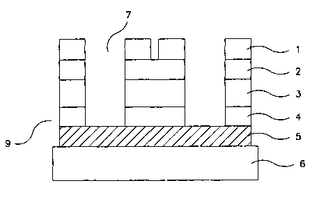
Figure 1 illustrates a schematic representation of a cross-section view of the
device
platform 9 of the present invention. The device 9 is built on a solid
supporting substrate 6,
which can be made of any solid, non-porous substance, including and preferably
glass,
plastic, ceramic, semiconductor or printed circuit board (PCB). Patterned
conductive
electrodes 5 are fabricated on top of the solid supporting substrate. The
patterned
conductive electrodes 5 are fabricated of electrically-conductive metals
(including but not
limited to transition metals such as aluminum, gold, copper, silver, platinum,
chromium,
and titanium), transparent conductors (such as indium-tin-oxide and zinc
oxide),
conductive plastics (such as polymers like polythiophenes, polyanilines,
polypyrroles, and
metal impregnated polymers), or conductive carbon (such as graphite).
1 S The devices are advantageously formed by standard fabrication techniques
used in
semiconductor manufacturing. Non-limiting examples of methods for producing
solid
substrates comprising the device platforms of the invention include but are
not limited to
thermal evaporation, wire bonding, metallization (evaporation, plating,
sputtering over a
shadow mask), dielectric deposition (by plasma, chemical vapor deposition or
sputtering ),
wet or dry chemical etching, reactive ion etching, or liftoff after the
desired pattern has
been defined using conventional photolithography.
A layer of insulative dielectric material 4, which can be made of polymers,
metal
oxide or nitrides such as SiO~, SiNX or AIOX is placed on top of the patterned
conductive
electrodes 5. An optional layer of conductive metal 3 is placed over the
insulative
dielectric material 4. This layer constitutes a reference electrode. In a
preferred
embodiment, the conductive metal layer 3 is silver, which is then
advantageously
converted to silver /silver chloride at a later stage in manufacturing. A
second layer of
insulative dielectric material 2 is then placed on top of the conductive
electrode layer 3. In
embodiments not comprising a reference electrode 3, a continuous dielectric
layer 2
comprising layers 2 and 4 as set forth herein are deposited. The second layer
of insulative
dielectric material 2 is optionally made of the same materials as the
insulative layer 4.
Patterned conductive electrodes 1 constructed on top of the second layer of
insulative dielectric material 2 constitute the final layer of each
addressable site in the
CA 02393766 2002-06-07
WO 01/43870 PCT/US00/34222
device 9. Well structures 7 are fabricated from this device by conventional
photolithography or laser drilling methods used in the semiconductor industry
for PCB
manufacturing. These wells can have rectangular, circular, trapezoidal or
other polygonal
openings. Additionally, the well walls may be either straight or curved, and
may have an
arbitrary angle with respect to the bottom electrode 5. An optional center
electrode can
alternatively protrude into the well area, as shown in Figure 3.
Figure 2 illustrates a schematic representation of a top view of the apparatus
of the
invention. The conductive electrodes 1 are preferred to be oriented in a
direction
orthogonal to the patterned conductive electrodes 5, generating row (i.e.,
patterned
electrodes 5) and column (i.e., conductive electrodes 1) addressable high-
density
electronic or electrochemical mini-cells (i.e., well structures 7) with
optional reference
electrodes built in-between. The well structure is preferably produced wherein
the bottom
of the well structure comprises the top of electrode 5 surface, while the top
of the well
structure is surrounded by the second electrode 1.
The proposed device 9 can be used as an x-y addressable, high-density biochip
array when biological probes 10 are immobilized on the patterned electrodes 5
inside each
well structure 7. The apparatus is capable of detecting changes in the
electrical properties
of the probes 10 in each well structure arising from the interaction of the
probes 10 with
target molecules 11. Though the inventive apparatus is useful for single
species detection,
where only a few test wells (low density) are required, the advantages of the
invention are
more pronounced in a high density array where hundreds, thousands, or millions
of test
wells are integrated in one array.
In a preferred embodiment, the probe molecules may be oligonucleotides,
nucleic
acids (such as DNA or RNA), proteins, peptides, antibodies or small molecules
such as
ligands, wherein probe molecules are chemically modified to contain anchoring
groups
that permit immobilization. Preferred modifications to the oligonucleotides
useful in the
practice of the invention include but are not limited to -OH, -NH2, -SH, -COOR
(where R
= H, lower (C,_,2) alkyl, aryl, heterocyclic alkyl or aryl, or a metal ion), -
CN, or -CHO.
Immobilization of such derivatized probes is accomplished by direct attaching
of the probe
molecules on the electrode surface through a functional group such -OH, -SH, -
NH2.
Alternatively, probe molecules can be efficiently immobilized on the electrode
surface through an intermediate species, termed a "spacer." In these
embodiments, the
surface of the electrode 5 is first modified with an intermediate species that
carries
-g_
CA 02393766 2002-06-07
WO 01/43870 PCT/US00/34222
functional groups such as hydroxyl (-OH), amino (-NHZ), thiol (-SH), carboxyl
ester (-
COOR, where R = H, lower (C,_,2) alkyl, aryl, heterocyclic alkyl or aryl, or a
metal ion),
nitrite (-CN), or aldehylde (-CHO), which can react with the probe molecules
functionalized with complementary members of the aforementioned anchoring
groups.
In another embodiment, the surface of the electrodes 5 is covered with a layer
of
polymer matrix. In these embodiments, probe molecules are attached onto a
supporting
matrix on the surface of the electrodes using the functional chemistry
mentioned above.
The polymer matrix is preferably selected to be polypyrrole, polythiophene,
polyaniline,
polyacrylamide, agarose gel, polyethylene glycol, cellular, sot gels,
dendrimers, metallic
nanoparticles, carbon nanotubes, and their copolymers. To increase the probe
loading
capacity, porous matrix such as polyacrylamide, agarose, or sot gels are
preferred.
Electronic or electrochemical detection of molecular interactions between
probe
and target molecules is achieved by devices having the structure, for example,
as depicted
in Figure 1. The electric or/and electrochemical methods used to interrogating
the
1 S biomolecule targets may be selected from, but are not limited to, AC
impedance, cyclic
voltammetry (CV), pulse voltammetry, square wave voltammetry, AC voltammetry
(ACV), hydrodynamic modulation voltammetry, potential step method,
potentiometric
measurements, amperometric measurements, current step method, and combinations
thereof.
In an alternative embodiment, an active driving circuit such as the one used
in an
active matrix liquid crystal display device can be built underneath or nearby
each test well
site to replace the electronic column and row drivers for x-y addressing such
as the one
used in the passive matrix liquid crystal display device.
In the practice of the invention, a high-density, x-y addressable probe array
is
exposed to an electrolyte solution containing a target molecule for a time and
under
conditions sufficient for the target to bind to a probe present in at least
one of the
particular addresses of the column-and-row addressable array. A voltage
potential or
other electric signal is applied to the each of the electrodes comprising each
of the
addressable sites through the x-y addressable column and row electrodes.
Changes in the
electrical properties or electrical signals from a particular electrode at a
particular site in
the x-y addressable array arising from interactions between probe molecules on
the
electrode and target molecules in the solution are detected to determine the
presence and
concentration of the target molecules in the solution.
_9_
CA 02393766 2002-06-07
WO 01/43870 PCT/US00/34222
In certain advantageous embodiments, electrical cross-talk between electrodes
is
reduced or eliminated in the x-y addressable array during target interrogation
with an
external electrical source. In these embodiments, the electrodes at the top of
the wells are
covered with an array of microfluidic channels. These channels are designed to
be
independently isolated from each other, with each having its own isolatable
liquid inlet
and outlet port. In addition to functioning as an electrical isolator, the
channels also act as
containers or reaction chambers for liquid during probe-target hybridization,
enzymatic
reactions and target interrogation with the external electrical source. In an
active driving
array where the x-y addressable columns and rows are replaced by an active
driving circuit
built underneath or nearby each test well site, the microfluidic channels can
be replaced by
a single chamber that covers all the test sites with
Electrolyte solutions useful in the apparatus and methods of the invention
include
any electrolyte solution at physiologically-relevant ionic strength
(equivalent to about
O.15M NaCI) and neutral pH. Nonlimiting examples of electrolyte solutions
useful with
the apparatus and methods of the invention include but are not limited to
phosphate
buffered saline, HEPES buffered solutions, and sodium bicarbonate buffered
solutions. In
alternative embodiments useful for electrical detection methods provided by
the invention,
the electrolyte solution comprises metal cations or polymerized cations that
are ion
conductive and capable of reacting with probes or probe-target complexes.
The Examples, which follow, are illustrative of specific embodiments of the
invention, and various uses thereof. They are set forth for explanatory
purposes only, and
are not to be taken as limiting the invention.
EXAMPLE 1
Fabrication of a linear microarray with four wells
A linear test microarray with four wells was fabricated on a 3" inch silicon
wafer
as follows. A photograph of the array is shown in Figure 4.
The linear test array was fabricated by conventional photolithography in a
class
100 clean room and fabrication was performed using three layers of masks as
shown in
Masks 12 (Figure SA), 14 (Figure SB) and 16 (Figure SC).
A three inch silicon wafer was cleaned using a solution of NH40H:H20 (1:10
v/v),
rinsed with de-ionized water, and then dried using a stream of nitrogen at
room
temperature. On the top of the wafer, 2000 Si02 was deposited by conventional
- 10-
CA 02393766 2002-06-07
WO 01/43870 PCT/US00/34222
chemical vapor deposition technique.
The array was then prepared sequentially as follows.
1. Bottom Electrode Formation
After cleaning the Si02-prepared substrate using a solution of NH40H:H20 (1:10
v/v), a de-ionized water rinse, and drying with a stream of nitrogen as
described above, a
thick (5 micron) photoresist (PR) layer was spin-coated on the wafer through a
three stage
process of spin-coating and softbaking. Using Mask 12 (shown in Figure SA) to
protect
the portion of the substrate that forms the bottom electrode, the surface was
exposed to an
ultraviolet light source using a wavelength of 365 nm and an intensity of 6
mW/cm3.
Following this treatment, the PR was hardbaked and developed. After removal of
Mask
12, the following metals were deposited sequentially by evaporation: Ti (to a
thickness of
1.0 Angstrom), Au (to a thickness of 21,000 Angstrom), and Ti (to a thickness
of 500
Angstrom). After evaporative deposition of these metal layers, a liftoff
protocol was used
to produce the bottom patterned electrode.
2. Top Electrode Formation
After cleaning the bottom electrode-prepared substrate using a solution of
NH40H:H20 (1:10 v/v), a de-ionized water rinse, and drying with a stream of
nitrogen as
described above, the wafer was coated with a thick (8 micron) layer of PR, as
described
above. Using Mask 14 (Figure SB) to protect the portion of the substrate that
forms the
top electrode, the surface was exposed to an ultraviolet light source using a
wavelength of
365 nm and an intensity of 6 mW/cm3. Following this treatment, the PR was
hardbaked
and developed as described above After removal of Mask 14, the following
metals were
deposited sequentially by evaporation: Ti (to a thickness of 1.0 Angstrom) and
Au (to a
thickness of 21,000 Angstrom). After evaporative deposition of these metal
layers, a
liftoff protocol was used to produce the top patterned electrode, as described
above.
3. Well Structure Formation
After cleaning the top electrode-prepared substrate using a solution of
NH40H:H20 (1:10 v/v), a de-ionized water rinse, and drying with a stream of
nitrogen as
described above, the wafer was then coated with a 4 micron layer of PR. The
surface was
exposed to an ultraviolet light source using a wavelength of 365 nm and an
intensity of 6
CA 02393766 2002-06-07
WO 01/43870 PCT/US00/34222
mW/cm3. Following this treatment, the PR was hardbaked and developed as
described
above. The wafer was then subjected to buffer oxide etching solution (4:1)
until each well
opening was cleared. The PR was removed by placing in a Branson 4000
Sonicator.
It should be understood that the foregoing disclosure emphasizes certain
specific
embodiments of the invention and that all modifications or alternatives
equivalent thereto
are within the spirit and scope of the invention as set forth in the appended
claims.
- 12-