Language selection

Search

Patent 2395080 Summary

Third-party information liability

Some of the information on this Web page has been provided by external sources. The Government of Canada is not responsible for the accuracy, reliability or currency of the information supplied by external sources. Users wishing to rely upon this information should consult directly with the source of the information. Content provided by external sources is not subject to official languages, privacy and accessibility requirements.

Claims and Abstract availability

Any discrepancies in the text and image of the Claims and Abstract are due to differing posting times. Text of the Claims and Abstract are posted:

  • At the time the application is open to public inspection;
  • At the time of issue of the patent (grant).
(12) Patent: (11) CA 2395080
(54) English Title: MULTILAYER PRINTED BOARD
(54) French Title: CARTE A CIRCUIT IMPRIME ET A PLUSIEURS COUCHES
Status: Term Expired - Post Grant Beyond Limit
Bibliographic Data
(51) International Patent Classification (IPC):
  • H05K 01/03 (2006.01)
  • H05K 03/46 (2006.01)
(72) Inventors :
  • SCHEEL, WOLFGANG (Germany)
  • KRABE, DETLEF (Germany)
  • CYGON, MANFRED (Germany)
  • DIETZ, MATHIAS (Germany)
(73) Owners :
  • FRAUNHOFER-GESELLSCHAFT ZUR FOERDERUNG DER ANGEWANDTEN FORSCHUNG E.V.
(71) Applicants :
  • FRAUNHOFER-GESELLSCHAFT ZUR FOERDERUNG DER ANGEWANDTEN FORSCHUNG E.V. (Germany)
(74) Agent: OYEN WIGGS GREEN & MUTALA LLP
(74) Associate agent:
(45) Issued: 2006-10-17
(86) PCT Filing Date: 2000-12-21
(87) Open to Public Inspection: 2001-06-28
Examination requested: 2003-11-21
Availability of licence: N/A
Dedicated to the Public: N/A
(25) Language of filing: English

Patent Cooperation Treaty (PCT): Yes
(86) PCT Filing Number: PCT/EP2000/013121
(87) International Publication Number: EP2000013121
(85) National Entry: 2002-06-17

(30) Application Priority Data:
Application No. Country/Territory Date
199 61 842.9 (Germany) 1999-12-21

Abstracts

English Abstract


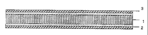
Disclosed is a multilayer printed board to be provided with electronic
components, which
has at least one layer whose thermal expansion behavior corresponds
approximately to
the thermal expansion behavior of the electronic components while at the same
time
substantially determining the thermal expansion behavior of the multilayer
printed board.


French Abstract

Carte à circuit imprimé et à plusieurs couches, destinée à être équipée de composants électroniques. Ladite carte comporte au moins une couche dont le comportement de dilatation thermique correspond à peu près au comportement de dilatation thermique des composants électroniques et détermine en même temps pour l'essentiel le comportement de dilatation thermique de la carte à circuit imprimé et à plusieurs couches.

Claims

Note: Claims are shown in the official language in which they were submitted.


6
What Is Claimed Is:
1. Method of manufacturing a multi-layer pc board for the assembly of
electronic devices,
which comprises at least one layer whose thermal expansion properties
correspond approximately
to the thermal expansion properties of the electronic devices and, at the same
time, determine
essentially the thermal expansion properties of the multi-layer pc board,
wherein
a thin glass foil (1) configured as borosilicate glass layer, having a
thickness of 30 µm to
1100 µm, is joined by means of a resin formulation (2) to a further
laminate (3) of the multi-layer
pc board by pressing so as to form a laminate.
2. Method according to claim 1, characterised in that a thickness in the range
from 50 to 500
µm is selected as thickness of said thin glass foil (1).
3. Method according to claim 1 or 2, characterised in that thermoplastic or
thermosetting
materials, metals or electrically conducting or non-conducting synthetic
resins are used as
laminates (3).
4. Method according to any of the claims 1 to 3, characterised in that said
thin glass foil (1)
is disposed inside or as outside layer of said multi-layer pc board.
5. Method according to any of the claims 1 to 4, characterised in that said
thin glass foil (1)
is used as reinforcing material for laminates and prepregs and/or as outside
layer in combination
with thermoplastic or thermosetting polymers.
6. Method according to any of the claims 1 to 5, characterised in that said
layer is perforated,
rendered porous, structured for optical applications, imprinted, physically
coated, chemically
coated, processed in a roll-to-roll process and/or thermally moulded.

Description

Note: Descriptions are shown in the official language in which they were submitted.


CA 02395080 2002-06-17
PCT/EP00/13121
Multilayer Printed Board
Technical Field
The present invention relates to a multilayer printed board to be provided
with electronic
components.
State of the Art
The increasing demand for electronic devices, greater function demands,
miniaturization
of components, which is closely linked to the further development in the
component
sector, and the demand for greater reliability have led to a wide spectrum of
printed
boards.
Particularly important for this is the printed board's dimensional stability
(constant
dimensions) if the board is exposed to thermal shock stress. The expansion
coefficient a
is considered as the criterium for the dimensional stability in dependence on
temperature. For FR quality (fiber glass fabric/epoxy resin) printed board
substrates, the
expansion coefficient is 16-18 ppm/K. The expansion coefficient for SI chips
is 3 ppm/K.
Thus it is impossible to mount semiconductor chips directly on printed boards
without
additional aids (e.g. uriderfilling) and further development of printed boards
for future
system integration is therefore very restricted. In view of this situation,
the structure of
molded laminated materials must be modified in such a manner that their
expansion
coefficient corresponds approximately to the expansion coefficient of silicon.
Employed as a carrier material for molded laminated materials are paper and
glass silk
fabric, more rarely glass silk mats, nonwoven glass fiber and quartz-fiber-
based fabric
as well as aramide-fiber-based fabrics. The most common binder is an epoxy
resin. If
there is thermal shock stress during mounting or during operation, differences
in the
thermal longitudinal expansion coefficients of materials lead to thermally
induced
mechanical tensions in the circuit carrier as well as at the points of
connection and at the

CA 02395080 2002-06-17
PCT/EP00/13121 2
points of contact, which lead to fatigue at the points of contact and in
extreme cases to
breaks in contact.
Typical examples of this problem are the differences in the expansion
coefficients of an
epoxy resin glass fabric as the base material for printed boards mounted with
bare
silicon chips respectively SMD components. When soldering, the difference
between the
longitudinal expansion coefficients in z-direction in the epoxy resin glass
fabric can lead
to tears in the metallization of the holes.
In order to overcome this problem, the expansion coefficients of the
connection
components have to be matched. Possible methods in use relating to fatigue at
the
points of contact are elastic connection component elements and underfilling
bare chip
structures.
The first possibility is not feasible with two-dimensional connections and the
second
possibility is an additional complicated process step.
Moreover, the integration of micronic function structures in multilayer
printed boards is
very expensive and complicated to realize.
Description of the Invention
The object is to provide a multilayer printed board which has greater
dimensional
stability, as a result of which the connections to the electric components
should be
exposed to less thermal expansion stress.
The solution is set forth in claim 1. Advantageous further improvements of the
present
invention are the subject matter of the subclaims.
In order to master the problem, a printed board having greater dimensional
stability is
proposed which not only eliminates the basic drawbacks of the previous method
of
2

CA 02395080 2002-06-17
PCT/EP00/13121
proceeding while making a substantially higher degree of system integration
possible,
e.g. with micronic function elements (optical, mechanical...).
An element of the present invention is that the multilayer printed board to be
provided
with electronic components has at least one layer whose thermal expansion
behavior
corresponds approximately to the thermal expansion behavior of the electronic
components while at the same time substantially determining the thermal
expansion
behavior of the multilayer printed board.
Especially suited is glass, particularly in the form of a thin glass film.
Such type suited
thin glass films can be obtained, for example, from the German firm DESAG
under the
item number AF45 and D263. Such type thin glass films are, in particular,
borosilicate
glass layers having a typical layer thickness of between 30 wm and 1.1 mm.
Preferably
suited for the aforementioned purpose, however, are thin glass films with
thicknesses
between 50 and 500~.m.
Other layer materials, such as glass composite materials or semiconductor
materials,
preferably the materials of which the components themselves are made, for
example SI,
can of course also be used.
Brief Description of the Invention
The present invention is made more apparent by way of example in the following
using a
preferred embodiment with reference to the accompanying drawing without the
intention
of limiting the overall inventive idea.
Fig. 1 shows a cross section of a multilayer arrangement.
Ways to Carry Out the Invention, Commercial Applicability

CA 02395080 2002-06-17
PCT/EP00/13121 4
By means of pressing, a laminate is produced from a 1 OOwm thick glass film (1
) together
with a special epoxy-resin-based resin formula (2) and a 18wm thick copper
foil (3). The
laminate has an overall thickness of 160~m.
The expansion of the laminate was measured under a constant load (100mN) by
means
of thermomechanical analysis (TMA) in dependence on temperature. The heating
up
time was 10°C/min.
The following values were determined for the expansion coefficients a:
-a1 (from 40/°C to T9) 6.2 ppm/°C
-a2 (from Tg to 195°C) 4.3 ppm/°C
-a3 (from 40°C to 195°C) 5.3 ppm/°C
4

CA 02395080 2002-06-17
PCT/EP00/13121
List of Reference Numbers
i glass film
2 resin layer
3 copper layer

Representative Drawing
A single figure which represents the drawing illustrating the invention.
Administrative Status

2024-08-01:As part of the Next Generation Patents (NGP) transition, the Canadian Patents Database (CPD) now contains a more detailed Event History, which replicates the Event Log of our new back-office solution.

Please note that "Inactive:" events refers to events no longer in use in our new back-office solution.

For a clearer understanding of the status of the application/patent presented on this page, the site Disclaimer , as well as the definitions for Patent , Event History , Maintenance Fee  and Payment History  should be consulted.

Event History

Description Date
Inactive: Expired (new Act pat) 2020-12-21
Letter Sent 2020-08-31
Inactive: COVID 19 - Deadline extended 2020-08-19
Inactive: COVID 19 - Deadline extended 2020-08-06
Inactive: COVID 19 - Deadline extended 2020-07-16
Inactive: COVID 19 - Deadline extended 2020-07-02
Inactive: COVID 19 - Deadline extended 2020-06-10
Letter Sent 2019-12-23
Common Representative Appointed 2019-10-30
Grant by Issuance 2006-10-17
Inactive: Cover page published 2006-10-16
Pre-grant 2006-07-26
Inactive: Final fee received 2006-07-26
Notice of Allowance is Issued 2006-03-28
Letter Sent 2006-03-28
Notice of Allowance is Issued 2006-03-28
Inactive: IPC assigned 2006-03-22
Inactive: Approved for allowance (AFA) 2006-01-13
Amendment Received - Voluntary Amendment 2005-12-07
Amendment Received - Voluntary Amendment 2005-11-23
Inactive: S.30(2) Rules - Examiner requisition 2005-09-13
Letter Sent 2003-12-09
All Requirements for Examination Determined Compliant 2003-11-21
Request for Examination Requirements Determined Compliant 2003-11-21
Request for Examination Received 2003-11-21
Letter Sent 2003-07-30
Inactive: Correspondence - Transfer 2003-06-16
Inactive: Office letter 2003-05-08
Inactive: Single transfer 2003-02-26
Inactive: Courtesy letter - Evidence 2002-11-19
Inactive: Cover page published 2002-11-15
Inactive: Notice - National entry - No RFE 2002-11-13
Application Received - PCT 2002-09-05
National Entry Requirements Determined Compliant 2002-06-17
Application Published (Open to Public Inspection) 2001-06-28

Abandonment History

There is no abandonment history.

Maintenance Fee

The last payment was received on 2005-10-14

Note : If the full payment has not been received on or before the date indicated, a further fee may be required which may be one of the following

  • the reinstatement fee;
  • the late payment fee; or
  • additional fee to reverse deemed expiry.

Patent fees are adjusted on the 1st of January every year. The amounts above are the current amounts if received by December 31 of the current year.
Please refer to the CIPO Patent Fees web page to see all current fee amounts.

Owners on Record

Note: Records showing the ownership history in alphabetical order.

Current Owners on Record
FRAUNHOFER-GESELLSCHAFT ZUR FOERDERUNG DER ANGEWANDTEN FORSCHUNG E.V.
Past Owners on Record
DETLEF KRABE
MANFRED CYGON
MATHIAS DIETZ
WOLFGANG SCHEEL
Past Owners that do not appear in the "Owners on Record" listing will appear in other documentation within the application.
Documents

To view selected files, please enter reCAPTCHA code :


To view images, click a link in the Document Description column. To download the documents, select one or more checkboxes in the first column and then click the "Download Selected in PDF format (Zip Archive)" or the "Download Selected as Single PDF" button.

List of published and non-published patent-specific documents on the CPD .

If you have any difficulty accessing content, you can call the Client Service Centre at 1-866-997-1936 or send them an e-mail at CIPO Client Service Centre.


Document
Description 
Date
(yyyy-mm-dd) 
Number of pages   Size of Image (KB) 
Representative drawing 2002-06-16 1 15
Claims 2002-06-16 2 59
Abstract 2002-06-16 1 12
Description 2002-06-16 5 154
Drawings 2002-06-16 1 18
Claims 2005-11-22 1 37
Claims 2005-12-06 1 38
Representative drawing 2006-09-20 1 15
Notice of National Entry 2002-11-12 1 192
Request for evidence or missing transfer 2003-06-17 1 101
Courtesy - Certificate of registration (related document(s)) 2003-07-29 1 107
Acknowledgement of Request for Examination 2003-12-08 1 188
Commissioner's Notice - Application Found Allowable 2006-03-27 1 162
Commissioner's Notice - Maintenance Fee for a Patent Not Paid 2020-02-02 1 541
Courtesy - Patent Term Deemed Expired 2020-09-20 1 552
PCT 2002-06-16 10 452
Correspondence 2002-11-12 1 26
PCT 2002-06-17 5 206
Correspondence 2003-05-07 1 20
Correspondence 2006-07-25 1 35