Note: Descriptions are shown in the official language in which they were submitted.
CA 02395847 2002-06-27
WO 01/50407 PCT/CA01/00017
- 1 -
TITLE: A SYSTEM FOR MULTI-STANDARD RFID TAGS
FIELD OF THE INVENTION
The present invention relates generally to radio
frequency identification systems, and more particularly,
to a reader for a.radio frequency identification system
that can operate with different tags at different
frequencies using different protocols.
BACKGROUND OF THE INVENTION
In general an RFID tag system allows for objects to
be labeled with tags such that when the tag is passed
through the electromagnetic field of a
reader/interrogator the object can be identified by
reading the tag that is attached to the object. In use,
RFID tags are attached in a wide variety of methods
including being bolted to the item or simply glued to the
inside of existing packaging or labeling. They can be
encoded with a user-defined data at time of use, or pre-
coded at time of tag manufacture numbering system or even
a combination of both.
Radio frequency identification systems provide a
number of advantages over paper and ink labels, such as
bar code systems in that: a much greater degree of
automation is permitted; clear line of sight is not
required, tags can be obscured by dirt, paper, even other
objects or packaging; reading distances can be greater;
tags can be hidden either to protect the tag from damage
in use or for security reasons; and in the case of
read/write tags incremental information can be stored on
the tags such as PO#, expiry date, destination,
confirmation of an applied process, etc.
Those are just some of the advantages of RFID tags.
CA 02395847 2002-06-27
WO 01/50407 PCT/CA01/00017
- 2 -
The tag may be a single integrated circuit chip bonded to
a flat, printed antenna, or could be a complex circuit
including battery and sensors for temperature, position,
orientation or any other required feature.
Specifically there are a great deal of different tag
types that can be characterized as having one or more,
but not limited to the following properties: passive,
having no battery and therefore receiving all of its
power required for operation from an electromagnetic
field transmitted by the reader/ interrogator or active
using a self contained battery on the tag; collision
arbitration, meaning that more than one tag can be read
in the field of a single reader/interrogator at one time
or non collision, meaning that only one tag can be in the
field of the reader/interrogator at a time in order to
insure a good read; multiple frequency where the data
from the tag is carried on a different frequency from the
data to the tag or single frequency where the carrier in
both directions is the same; full duplex, where the tag
is transmitting data back to the reader/interrogator
while the reader/interrogator's transmitter is active or
half duplex where the tag waits for the
reader/interrogator's transmitter to go inactive before
replying; solicited, where the tag must be commanded by
the reader/interrogator before it transmits the data
back, or unsolicited, where the tag transmits back as
soon as it is powered up; active transmitter, where the
tag has its own oscillator and transmitter or back-
scatter, where the tag modulates the field set up by the
reader/interrogator's transmitter; read only tag, which
can be equated to an electronic barcode or read/write
tag, which allows for the equivalent of a scratch pad on
the tag. In either case tags can have different sizes of
data that is transferred, different sizes of write-able
CA 02395847 2002-06-27
WO 01/50407 PCT/CA01/00017
- 3 -
memory, different accessing schemes to the data and
different methods of writing; carrier frequency, is a
function of the application, the physics of the objects
being tagged, the range required and the radio frequency
spectrum regulations of the country in which it is
operating; data rate, is a function of the carrier
frequency, the application needs and the radio frequency
spectrum regulations .of the country in which it is
operating; data encoding methods can vary significantly
however some form which encodes the data with the clock,
such as Manchester encoding is generally used; packet
protocol for data transmission from and to the tag has to
be defined in terms of headers, addressing, data field
types and sizes, commands, functions, handshaking, etc.
etc. ; error correction or detection codes, can be used by
the tags to improve reliability of the tag data transfer,
generally a CRC error detection only scheme is used,
however the particular CRC code must be specified,;
additional signaling devices such as beepers or LEDs can
be added.to the tag to alert and direct the operator to
a particular tagged object in the field; additional
sensors, such as, for example temperature, can be added
to the tag to record extreme conditions that the tagged
object has been passing through.
As can be seen from the list above, there is an
extremely wide variety of tag types that may be used or
required by an application making it very hard to have
one reader/interrogator handle all tag types. Typically
there would have to be a specific reader/interrogator
matched to the specific properties of each type of tag
being used in the application.
For example, a typical low cost passive tag system
with unsolicited tag response, would be implemented as
CA 02395847 2002-06-27
WO 01/50407 PCT/CA01/00017
- 4 -
follows; the reader/interrogator would first activate
the tag by generating an electromagnetic field of a given
frequency. Such an electromagnetic field can be
generated, for example, by applying an alternating
electrical current at a given frequency to a coil for low
frequency near field systems commonly called inductively
coupled systems or to an RF antenna for far field higher
frequency systems.
The tag includes an antenna, which could be a dipole
for far field systems or a coil for inductive systems
tuned to the frequency of the interrogator's generated
electromagnetic field. The electrical current thus
generated in the tag's antenna is used to power the tag.
Data is generally sent to the tag by modulating this
interrogator generated electromagnetic field which is
commonly called the exciter or illuminating field. The
tag can send data back to the interrogator either by
transmitting with its own transmitter with a separate
frequency and antenna from the illuminating field or by
modulating the illuminating field by changing the loading
of the tag's antenna in what is commonly called a back
scatter system. In any case, either the new
electromagnetic field from the tag or the disturbances in
the interrogator's illuminating field caused by the tag's
back scatter system is detected by the interrogator. The
data from the tag is thus decoded, thereby enabling the
tag and the item to which the tag is attached to be
identified. In some cases written to, as in the case of
read/write tags by modulating the interrogator's
generated electromagnetic field. Typical information
that might be stored on the tags would be: PO#; expiry
date; destination; confirmation of an applied process,
etc.
CA 02395847 2002-06-27
WO 01/50407 PCT/CA01/00017
- 5 -
The advantages and disadvantages of using different
properties for the tag depend so heavily on the type of
application that at this point there is no clear winner
type of tag that will totally dominate the field. For
example, in some cases range is an advantage, in .other
cases range is a disadvantage. Objects with high
moisture or water content are not suitable for tagging
with high frequency tags. Applications requiring high
data rates or many tags in the field at any one time are
not suitable to low frequency tags. Cost of,the tag in
relationship to the object being tagged and or the re-
usability of the tag is a very important constraint in
selecting tag properties.
As can be seen even from the few examples shown
above, any application will be a compromise of tag
properties in order to meet the application's need. In
order to maximize the performance and meet the cost
goals, the type of tag must be selected to match the
application. Even if a single carrier frequency can be
selected for an application differences in the other
properties of the tag could still necessitate different
reader/interrogators for the different tag types. Given
that this is the case and that any large application may
have different performance goals and therefore tag types,
it is extremely advantageous to have a
reader/interrogator that is flexible and can read many
tag types simultaneously. This might even be mandatory
in applications where there are different
reader/interrogator types operating at the same carrier
frequency and thus interfering with each other-. Such a
universal reader/interrogator would also solve the other
great hurdle in implementing RFID tag systems, and that
is the ,fear of obsolescence and not being able to read
the next type of tag that may be required in the
CA 02395847 2002-06-27
WO 01/50407 PCT/CA01/00017
- 6 -
application.
In some situations, it is possible for an end user
of the radio frequency identification system to include
multiple readers, so that different tags using different
protocols can be read. However, this is inefficient and
expensive, as multiple readers would not be required if
a single common standard for tags were used.
Furthermore, multiple readers are likely to interfere
with each other, especially if they operate at common
radio frequencies.
Prior art readers for radio frequency identification
systems have been devised to address some of the above-
mentioned problems. For example, International patent
application No. PCT/US98/10136, filed by AVID
Identification Systems, Inc., on 14 May 1998, and
entitled READER FOR RFID SYSTEM discloses a reader for
reading tags of different protocols in a radio frequency
identification system. According to this system, the
identification signal from the tag is sensed by the
inductive coil of the reader as described above in that
the voltage across the coil is modulated in accordance
with the code sequence programmed into the tag. The
signal received by the coil is sent to a central
processing unit for processing and decoding, where the
signal is first analyzed by measuring the pulse width of
the signal. The central processing unit then selects a
tag protocol that is most likely to be the correct
protocol based on the pulse width that has been measured.
The AVID radio frequency identification system may
suffer from a number of shortcomings. For example, while
the radio frequency identification system provides for
reading of tags using different protocols in the same
CA 02395847 2002-06-27
WO 01/50407 PCT/CA01/00017
frequency range, it does not permit tags operating at
different frequencies to be read by the same reader as
the inductive coil of the reader is not operable for all
electromagnetic frequencies. The AVID system is
essentially an inductive based arrangement operating at
a single frequency. Furthermore, the AVID system does
not accommodate all of the tag properties and
characteristics described above. Because the AVID system
measures a single pulse width, at worst the system can
only infer data rate from the pulse width and at best the
system can only select from a very small group of tag
types where the tag type would only be suitable if it has
a distinguishing header pulse width. In general, the
AVID system is not suitable for multiple carrier
frequencies.
In view of the foregoing, there still remains a
reader for a radio frequency identification system that
may be used with tags operating at different frequencies
with different protocols.
SUMMARY OF THE INVENTION
The present invention provides a reader/interrogator
for a radio frequency identification system which is
suitable for use with tags operating. at' different
frequencies and also with different tag operating
properties, such as data protocol, encoding, data rates,
and functionality as introduced above.
The reader/interrogator system according to the
invention divides the problem of multiple tag types into
two classes. The first class is characterized by
carrier frequency and the second class is characterized
by the tag operating parameters. The first class may be
broadly broken down into four principal frequency bands
CA 02395847 2002-06-27
WO 01/50407 PCT/CA01/00017
_ g _
that are in common use today. Each of these bands, on
its own, requires its own antenna configuration,
transmitter and receiver appropriate to the frequency of
operation. This frequency dependent component is
referred to as an RFM or radio frequency module.
The second class is defined as the remaining tag
operating parameters, sometimes grouped together and
referred to as protocol, and are considered as
, computational problems. This is handled by another
component of the invention referred to as the ICM or
interrogator control module. This module either directly
calculates the parameters from the incoming tag signal,
such as data rate, message~length and encoding scheme or
exhaustively tries either in parallel or serial the
possible remaining parameters, such as type of CRC used.
The results of the parameter determinations are verified
against a list of acceptable tag parameter combinations
before passing on the decoded data as a valid message.
The reader/interrogator according to the invention
simultaneously handles tags operating at different
carrier frequencies by utilizing a separate RFM for each
required carrier frequency connected to an ICM. The data
being passed between the RFM and ICM is stripped of any
carrier frequencies and is processed by the ICM in a like
manner regardless of which frequency band the tag is
operating in. The carrier frequency or RFM from which
the tag data is received is only used as one of many
parameters to specify a tag type from the last of valid
tag type parameter combinations.
In addition, multiple RFMs operating at the same
carrier frequency may be used with a single ICM where the
application requires a special shaping of the field or
CA 02395847 2002-06-27
WO 01/50407 PCT/CA01/00017
- 9 -
multiple antenna orientations or polarizations in order
to read all the tag configurations. In this case the
single ICM removes any problems of interference that
would arise from having two separate reader/interrogators
trying to handle the collision arbitration and commands
to a tag that might be picked up by both units
simultaneously. It also prevents having the strong
signal from one reader/interrogator totally wiping out
any low level return signal from a tag which would
otherwise only be visible to another reader/interrogator.
In accordance with one aspect of the present
invention, there is provided an interrogator for a radio
identification system having a number of tags, with
selected tags operating at a first frequency, and other
tags operating at another frequency, the interrogator
comprises: (a) a first radio frequency module having a
transmitter for transmitting an output signal at the
first frequency to the tags, and including a receiver for
receiving return signals transmitted by the tags
operating at the first frequency; (b) a second radio
frequency module having a transmitter for transmitting an
output signal at the second frequency to the tags, and
including a receiver for receiving return signals
transmitted by the tags operating at the second
frequency; (c) a controller module coupled to the first
and second radio frequency modules, the controller module
including a controlling for controlling the transmitters
for transmitting the output signals to the tags, and
including a decoder for decoding the return signals
received from the tags.
BRIEF DESCRIPTION OF THE DRAWINGS
Reference will now be made, by way of example, to
the accompanying drawings, which show a preferred
CA 02395847 2002-06-27
WO 01/50407 PCT/CA01/00017
- 10 -
embodiment of the present invention, and in which:
Fig. 1 is a block diagram showing a reader according
to the present invention for a radio frequency
identification system;
Fig. 2 is a block diagram showing a conventional tag
suitable for use with the reader according to the present
invention;
Fig. 3(a) is a block diagram showing a reader
frequency module for the reader according to the present
invention;
Fig. 3(b) is a block diagram showing an interrogator
control module for the RFID reader according to the
present invention;
Fig. 4(a) is a schematic diagram showing in more
detail the front-end of the reader frequency module of
Fig. 3 (a) ; and
Fig. 4(b) is a schematic diagram showing in more
detail the rear-end of the reader frequency module of
Fig. 3 (a) .
DETAILED DESCRIPTION OF THE PREFERRED EMBODIMENT
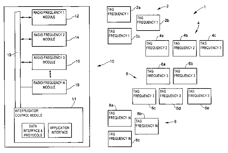
Reference is first made to Fig. 1 which shows a
multiple-frequency/protocol RFID tag reader according to
the present invention and indicated generally by
reference 10. The multiple-frequency/protocol RFID tag
reader 10 provides the interrogator in a radio frequency
identification ("ID") system 1. As shown in Fig. 1, the
radio frequency identification system or RFID 1 comprises
a plurality of tags. In conventional RFID systems the
CA 02395847 2002-06-27
WO 01/50407 PCT/CA01/00017
- 11 -
tags in the field for a reader all operate at the same
frequency with the same tag parameters. As will be
described, the- reader 1 according to the present
invention is suitable for interrogating tags operating at
different frequencies in the radio frequency field.
The reader or interrogator 10 as shown in Fig. 1 is
operable with four different frequency types of tags 2,
4, 6 and 8. The first type of tags 2, shown individually
as 2a, 2b and 2c, operate at a first frequency, for
example, 125 KHz. The second type of tags 4, shown
individually as 4a, 4b, and 4c, operate at a second
frequency, for example, 13.56 MHz. The third type of tags
6, shown individually as 6a, 6b, 6c, 6d and 6e, operate
at a third frequency, for example, 869 MHz. The fourth
type of tags 8, shown individually as 8a, 8b and 8c,
operate at a fourth frequency, for example, 2 . 45 GHz . It
will be appreciated that while the reader 10 according to
the present invention is described in the context of four
types of tags, the reader 10 is suitable for operation
with tags operating at other frequencies and with
differing operating parameters whether at the same or
different frequency.
In the industry, radio frequency identification tags
generally come in four different frequency bands, 100-200
KHz., 13.56 MHz., 450-869-917 MHz. and 2.45 GHz. As will
be understood, all four bands have different physical
properties which make the tags suitable for specific
applications and environments.
The first frequency band, i.e. 100-200 KHz., is
suitable for tagging containers holding liquids and also
for tagging the human body. These radio frequency fields
can be well defined and well contained. The first
CA 02395847 2002-06-27
WO 01/50407 PCT/CA01/00017
- 12 -
frequency band, however, is suitable only for short
ranges, typically less than one meter. Moreover, the
first frequency band is only capable of very low data
rates and therefore provides poor performance in
applications requiring multiple tags to be read.in the
radio frequency field at the same time.
The second frequency band, i.e. 13.56 MHz., is
commonly used for short range passive tags. It is
generally inductively coupled in the tag since the
wavelength is too long for a practical far field antenna.
Like the first band, the range is relatively short,.
approximately one meter. This frequency band is also
sensitive to the presence of water and de-tuned by the
human body.
The third band, i.e. 458-869-917 MHz., is commonly
used for long passive tags (e.g. half-duplex tags). The
wavelength in this band is short enough to use dipole
antennas and far field effects. This band is suitable
for long range tag applications, e.g. one-half watt of
power provides an approximate range of 10 to 15 feet.
This band also supports high data rates and with anti-
collision algorithms in the reader, numerous tags can be
supported at the same time. However, spacers or special
antennas must be utilized to tag metal objects, and these
tags are not suitable for tagging people or container of
liquid.
3 0 The fourth band, i . a . 2 . 45 .GHZ . , can support very
high data rates and is therefore suitable for multiple
tags operating in the radio frequency field. Also with
the high frequency, only a very small antenna geometry is
needed which results in a small footprint for the tag.
When compared to the other frequency bands, tags for this
CA 02395847 2002-06-27
WO 01/50407 PCT/CA01/00017
- 13 -
band are the most sensitive to water and people. Another
disadvantage is that these type of tags tend to utilize
expensive components in order to provide efficient field
operation.
Reference is made back to Fig. 1. To provide the
capability to operate with different types of tags 2, 4,
6 or 8, the reader 10 according to the present invention
comprises an interrogator control module 11, and a radio
frequency module for each different frequency of tag.
Differing types of tags, which have the same carrier
frequency, may use the same radio frequency module. As
shown in Fig. 1, the reader 10 includes a radio frequency
module 12 for reading the tags 2 operating at the first
frequency (e.g. 125 KHz.), a radio frequency module 14
for reading the tags 4 operating at the second frequency,
a radio frequency module 6 for reading the tags 6
operating at the third frequency (e.g. 13.56 MHz.), a
radio frequency module 16 for reading tags 6 operating at
the third frequency (e. g. 869 MHz.), and a radio
frequency module 18 for reading tags 8 operating at the
fourth frequency (e. g. 2.45 GHZ.). The radio frequency
modules 12, 14, 16, 18 provide the radio interfaces
between the respective tag types and the interrogator
control module 11.
As shown in Fig. 1, the radio frequency modules 12,
14, 16, 18 are coupled to the interrogator control module
11 through a bus 19. The bus 19 is implemented as a low
speed bus and provides control signals to the radio
frequency modules 12 to 18 for interrogating the
respective types of tags 2 to 8 and data signal for
receiving information transmitted by the tags to the
respective radio frequency modules. By utilizing such an
arrangement, the radio frequency modules are arranged in
CA 02395847 2002-06-27
WO 01/50407 PCT/CA01/00017
- 14 -
parallel to provide a multi-frequency capability for the
reader 10, which is further adaptable by adding
additional radio frequency modules or replacing one or
more of the existing radio frequency modules 12, 14, 16
or 18 with radio frequency modules configured for other
frequency bands. In addition, a plurality of radio
frequency modules may be used at the same frequency band
where that might be required for shaping of the field or
for handling different tag orientations being presented
in the field. It will be appreciated that if multiple
radio frequency modules are being used in the same
frequency band, they should differ in the center
frequency sufficient to meet regulations and such that
the beat frequency between the two units is higher than
the maximum data rate.
Reference is next made to Fig. 2, which shows in
diagrammatic form the organization of a typical tag 20
according to the art. The tag 20 comprises a series of
modules including an air interface 21, logic 22, a power
supply 24. If the tag 20 is a read/write tag, there is
memory module 26. The air interface 21 provides a radio
frequency communication interface to the reader 10. The
logic 22 comprises conventional logic (i.e. digital
circuitry) that controls the other modules in the tag 20.
The power supply 24 provides local power to run the tag
20. In the majority of tags, i.e. passive tags, the
power supply 24 is energized by the RF signal received
from the reader 10. In active tags the power supply
circuit comprises a battery and an activation circuit.
If the tag 20 is read/writeable, then user defined data
may be stored in this memory and read back by the reader.
Depending on the tag properties, a particular tag might
be a write once device or it might be erasable and
rewritten many times (typically 10,000). Some tags may
CA 02395847 2002-06-27
WO 01/50407 PCT/CA01/00017
- 15 -
only be write-able via direct contact and not through the
RF interface, however, the reader provides the capability
to write the tags via the RF interface.
Referring next to Figs. 3(a) and 3(b), the radio
frequency module 12 and the interrogator control module
11, respectively, are shown in more detail. According to
this aspect of the present invention, the radio frequency
module 12 provides the radio interface to the associated
types of tags) 2, 4, 6 or 8. The radio frequency module
12 is a frequency dependent device, e.g. 100-200 KHz.,
13.56 MHz, 458-869-917 Mhz. or 2.45 GHZ. The radio
frequency module 12 and the tag(s)~ go together as one
type of unit (indicated as 13 in Fig. 3(a)), i.e. any
given tag frequency will have a dedicated radio frequency
module 12 in the reader 10. As shown in Fig. 3(a), the
radio frequency module 12 comprises an air interface
stage 31 and a data interface stage 32. Both the air
interface stage 31 and the data interface stage 32
comprise analogue circuitry as will be described in more
detail below with reference to Fig. 4. The data
interface stage 32 provides a data shaping function.
The interrogator control module 11 as described
above connects to and controls several types of radio
frequency modules 12, 14, 16 and 18 and tag types through
the bus 19 (Fig. 1). This arrangement according to the
present invention allows the reader 10 to read tags in
the same field which operate at different frequencies
and/or different operating parameters. As shown in Fig.
3(b), the interrogator control module 11 comprises a data
interface and protocols stage 34, and an application
interface stage 36.
The application interface stage 36 comprises a
CA 02395847 2002-06-27
WO 01/50407 PCT/CA01/00017
- 16 -
programmed microprocessor which interfaces to the data
interface and protocols stage 34 and controls the
operation of the interrogator control module 11 and the
individual radio frequency modules 12, 14, 16 and 18
through the bus 19. As shown in Fig. 3(b), the
interrogator control module 11 also includes a LCD touch
panel 38 for accepting user commands and displaying
information concerning the operation of the radio
frequency identification system 1, the radio frequency
modules 12, 14, 16 and 18, and the tag types.
Preferably, the program memory for the microprocessor in
' the application interface 36 is implemented using flash
memory thereby allowing programs to be downloaded from a
PC (not shown) via a conventional network connection.
The data interface and protocols stage 34 includes
circuitry for processing the receive signal output from
the data interface stage 32 (Fig. 3(a)) in-the radio
. frequency modules 12 (14, 16 and 18) . This processing
includes performing clock separation, recovering data
from the receive signal output, and the handling of data
protocols based the tag types being controlled. The data
interface and protocols stage 34 is preferably
implemented as a field programmable gate array or FPGA.
Advantageously, an implementation utilizing a field
programmable logic device allows the reloading of
different protocols under the control of the
microprocessor in the application interface 36. The FPLD
is programmed to accept the data rates and protocols
available on the various types of tags 2, 4, 6, or 8. In
operation, the microprocessor in the interrogator control
module 11 loads the FPGA with the appropriate
configuration data to handle data decoding and protocol
conversion for the tags which are to be interrogated in
the field. At this point the data is totally stripped of
CA 02395847 2002-06-27
WO 01/50407 PCT/CA01/00017
- 17 -
its carrier frequency component and other than being used
as an index into a list of acceptable tag types with
their possible operating parameters, the carrier
frequency is no longer used in the decoding. There are
tag families which use the same logic circuit and
therefore operating parameters regardless of the carrier
frequency. In this case the data interface and protocol
stage use the same procedure for decoding regardless of
which RFM the signal came in on. In some cases there
will be different tag types operating on the same carrier
frequency and the interface and protocol stage will use
different procedures even for signals coming in on the
same RFM.
The FPGA directly controls the transmitter for data
going back to the tag or for collision arbitration
signals going to the tags, since the FPGA has derived the
clock rate and timing required for the particular tag
type. The RFM and the microprocessor may also gate these
signals to have general control of the RFM's transmitter.
The ICM turns on the transmitters according to regulatory
and application requirements to power the passive tags
and/or to wake up the active tags and any polling
sequence that may be required for the tags types in use
is transmitted. The ICM then waits for the response
signals from the tags and determines the type of tag that
is in the field. The FPGA directly calculates a selected
parameter from the incoming tag signal, such as data
rate, message length and encoding scheme or exhaustively
tries either in parallel or serial the possible remaining
parameters, such as type of CRC used. The results of the
parameter determinations are verified against a list of
acceptable tag parameter combinations before passing on
the decoded data as a valid message.
CA 02395847 2002-06-27
WO 01/50407 PCT/CA01/00017
- 18 -
The FPGA is configured to handle all low level
communications to and from the tag via the air interface
stage 31 and the data interface stage 32 in the radio
frequency module 14. While the FPGA is programmed to
handle the low level communication, the microprocessor is
programmed to perform all higher level data protocol
conversions and the forwarding of processed data to the
user (i.e. via a LCD touch panel) or to a networked PC
using a standard communication protocol such as TCP/IP.
Preferably, the handling of data rate and data
encoding for the tags in the reader 10 is implemented as
a clock and data separation scheme utilizing a phase
locked loop on the incoming signal. This implementation
is advantageous since the tag rate can and will vary
during transmission and therefore measuring a single
pulse is generally not sufficient to yield an accurate
bit rate for the tag data. This yields a far better
result than just measuring the width of the leading pulse
in the message.
It will be understood that while accurately
determining the data rate of the tag message may be
sufficient to distinguish between the tag types on the
basis of different data rates, in general, this is not
sufficient to determine other operating parameters of the
tag.
The data and clock separation function. in the FPGA
presents the data to the protocol and error checking
function of the FPGA. Preferably the FPGA is implemented
to provide several protocols and CRC checks in parallel.
The path leading to a full check, or zero errors in
decoding is assumed to be the correct operating
parameters for that tag. The tag message along with the
CA 02395847 2002-06-27
WO 01/50407 PCT/CA01/00017
- 19 -
assumed tag type is presented to the microprocessor which
then determines if the type is in the list of acceptable
tag types. If so the tag data is passed on to the
application.
Reference is next made to Figs. 4 (a) and 4 (b) which
show in more detail the air interface stage 31 and the
data interface 32, respectively, for a radio frequency
module 12, 14, 16 and 18. In particular the figures
depict a far field effect type of RFM which uses an RF
antenna as opposed to a coil with inductive coupling.
This type of RFM is suitable for the high frequencies
such as UHF or higher. As shown in Fig. 4(a), the air
interface stage 31 comprises an antenna 101, a circulator
102, a transmitter 104, a mixer stage 106, and an
amplifier stage 108. Preferably, the mixer stage 106 and
amplifier stage 108 comprise a minimum of two channels
with a delay between them to allow for quadrature
. decoding of the signal. Additional channels and delays
could be added to allow the same RFM to~ be used at
different frequencies. Fig. 4(a) shows three channels,
which could allow for quadrature decoding of up to three
separate carrier frequencies. Each channel having a
corresponding mixer 107, shown individually as 107a, 107b
and 107c, and a corresponding amplifier 109, shown
individually as 109a, 109b, and 109c. As will be
understood by those skilled in the art, the three channel
configuration allows quadrature information to be
extracted for each tag. The transmitter 104 is coupled
to the antenna 101 through the circulator 102. In known
manner, the circulator~102 allows the antenna 101 to be
used for both transmitting signals to the tags 2 (4, 6,
and 8) and receiving signals from the tags 2 (4, 6, and
8 ) . The transmitter 104 generates a constant f field ( i . a .
the illumination or power signal) which provides power to
CA 02395847 2002-06-27
WO 01/50407 PCT/CA01/00017
- 20 -
each of the tags 2 associated with the radio frequency
module 12. The transmitter 104 also generates a
reference output signal that is fed to the mixer for each
of the channels as shown in Fig. 4 (a) . The mixer 107b
for the second channel includes a delay element 105a to
delay the feed of the reference output signal.
Similarly, the mixer 107c for the third channel includes
a delay element 105b to further delay the feed of the
reference output signal (received from the first delay
element 105a).
The mixer subtracts the carrier to produce a Non
Return to Zero image of the data that was modulated onto
the carrier by the tag. The signal from the mixer is AC
coupled to the amplifier stage to remove any DC component
that might be contained in the signal. This allows for
higher gains on the amplifiers. The signal is then
further differentiated to provide sharp pulses on the
leading and trailing edges of the data bits.
20. Advantageously, this allows for even higher amplification
stages and eliminates the, need for filtering between
stages according to the data rate, thus making the
channel suitable for a wide range of data rates. The
data interface stage 32 receives the output from the
amplifier stage 108 (i.e. the amplifier 109 for each of
the three channels) in the air interface stage 31. The
data interface stage 32 provides a pulse shaping
operation and comprises a pulse shaping circuit 110 as
shown in Fig. 4(b) for each of the three channels in the
air interface stage 31 (Fig. 4(a)). The pulse shaping
circuit 110 comprises a discriminator 111, a rectifier
circuit 112, a summing amplifier 114, a logic level
convertor 116 and a output port 118. The discriminator
111 comprises a capacitor which couples the output from
the amplifier 109a to the rectifier circuit 112. The
CA 02395847 2002-06-27
WO 01/50407 PCT/CA01/00017
- 21 -
discriminator 111 converts the output signal into pulses
with defined edges. The rectifier circuit 112 comprises
a pair of diodes which separate the pulses into positive
and negative edges. The positive and negative edges are
then summed together by the operational amplifier 114
resulting in a pulse for, each .edge. The logic level
convertor converts the level of the pulses for output.
The output port 118 to the bus 19 (Fig. 1) is implemented
using an opto-coupler device which advantageously
provides isolation and levelconversion between the
circuitry in the radio frequency module 12 ( 14 , 16 or 18 )
and the interrogator control module 11. The pulses are
then processed by a data protocol decoder in the data
interface and protocols stage 34 of the interrogator
control module 11.
The data decoder is implemented in the program (i.e.
firmware) executed by the microprocessor in the data
interface and protocols stage 34. The data decoder
provides the functionality to decode the pulse streams
received from the data interface stage 32 in the radio
l
frequency module 12 (14, 16 and 18). Utilizing the phase
locked loop clock and data separation scheme, the pulse
stream is decoded according to the protocol (e. g.
Manchester encoded)associated with the type of tag 2, 4,
6 or 8. The three output data channels in each radio
frequency module 12, 14, 16 anc~ 18 provide parallel paths
for the decoding the data received from the tags. The
programmed microprocessor performs code checking and CRC
decoding to select the tag data stream which does not
have any code violations and a successful CRC result.
In operation, the interrogator control module 11
initiates the interrogation of the tags through the radio
frequency module configured for the frequency band of the
CA 02395847 2002-06-27
WO 01/50407 PCT/CA01/00017
- 22 -
tags, for example, the second radio frequency module 14
(Fig. 1) .is configured for the 13.56 MHz tags 4. The
interrogation can be in response to an input from the
user entered on the LCD touch panel 38 or to a command
received from a networked PC. The interrogator control
module 11 sends a command (i.e. control signals) via the
bus 19 to the radio frequency module configured for the
tags being interrogated, for example, the radio frequency
module 14 for 13.56 MHz tags 4. In the radio frequency
module 14, the transmitter 104 (Fig. 4(a)) excites the
antenna 101 to transmit an interrogation or power signal
to the tags 4 in the field. At the sameltime, the
transmitter 104 also generates a reference output signal
for the mixer stage 106 (Fig. 4(a)) as described above.
The tags 4 tuned to the frequency of the radio frequency
module 14 receive and are energized by the interrogation
signal and after a short delay transmit their response
signals back to the radio frequency module 14. The
response signals are received by the antenna 101 and
reflected back and split into three channels for the
mixer stage 106 through the circulator 102. In the mixer
stage 106, the received signal is subtracted from the
transmitted signal to produce a phase shift. The output
from the mixer stage 106 is passed to the amplifier stage
108. ' The amplified signal is then shaped by the pulse
shaping circuit 110 (as described above with reference to
Fig. 4(b)) to generate a series of pulses in three
channels. The three channels of pulses are transferred
over the bus 19 to the data interface and protocols stage
34 of the interrogator control module 11. In the
interrogator control module 11, the data decoder (data
interface and protocols stage 34) uses a phase locked
loop Clock and data separation scheme to lock onto the
pulse stream, determine the protocol for the tag, and
extract the data transmitted by the tag. Code checking
CA 02395847 2002-06-27
WO 01/50407 PCT/CA01/00017
- 23 -
and application of CRC is also performed to ensure the
integrity of the data decoding.
The present invention may be embodied in other
specific forms without departing from the spirit or
essential characteristics thereof. Certain adaptations
and modifications of the invention will be obvious to
those skilled in the art. Therefore, the presently
discussed embodiments are considered to be illustrative
and not restrictive, the scope of the invention being
indicated by the appended claims rather than the
foregoing description, and all changes which come within
the meaning and range of equivalency of the claims are
therefore intended to be embraced therein.