Note: Descriptions are shown in the official language in which they were submitted.
CA 02395900 2002-08-12
FILE NO. PRIVILEGED AND CONFIDENTIAL
- 4 -
Field of the Invention
The invention relates to capacitor in integrated circuit technology.
Background of the Invention
Traditionally integrated circuit capacitors are made using parallel plates,
where each
conductive plate is on a different conductive layer separated by a special
thin oxide. Because
this requires special processing steps, not used in standard digital
circuitry, many designers are
forced to use metal interconnection layers, separated by standard dielectrics.
Parallel plate
capacitors using this method have a much lower density (capacitance per area)
and higher
parasitic capacitances than the specialized capacitance process.
Recently due to the shrinking dimensions in deep sub-micron processes,
designers have been
choosing to use the capacitance created by lateral flux within a single metal
layer [2]. Since
the minimum spacing between interconnect layers for deep sub-micron processes
is becoming
much smaller and better controlled than the dielectric thickness, the
capacitance density and
matching for this type of capacitor is better than a horizontal parallel plate
capacitor in the
same technology [1]. Other methods [5,6,7,8,9] have attempted to improve on
the capacitance
density, but the highest density capacitor is obtained by using interleaved
vertical posts or
fingers [1]. This structure is undesirable because it has high resistive
losses and uses two metal
interconnect layers for the connection of the fingers.
Both plates of the capacitor will experience parasitic capacitances to the
ground or power
2 0 connection of the integrated circuit. For many circuit designs it is
desirable to have both plates
of the capacitor exactly the same, i.e. with the same parasitic capacitance.
Furthermore, many
circuit designs rely on the matching of two different capacitors. Many
different techniques,
such as the use of fractal structures have been construed to improve the
matching of the
capacitors [5,6].
2 5 In integrated circuit technology, the photolithography used to create
conductive geometries will
deviate from the ideal. The amount of deviation varies from one chip to
another and within the
chip itself. Often, the deviation from the ideal of a geometry is related to
the direction of that
geometry. For example a conductor drawn on the x-axis may have a width 10 %
greater than
ideal, while an conductor intended to match, drawn on the y-axis may have a
width 10 % less.
3 0 It is desirable to have a structure that minimizes this variation by
averaging the offsets caused
by the different lithographic traces.
Summary of the Invention
There is therefore provided in a present embodiment of the invention a method
for creating
capacitors, using primarily the lateral flux with geometries which allow good
matching
3 5 between the two plates of the capacitor and from one capacitor to another.
The invention involves the use of a plurality of lateral flux capacitors in
varying orientation,
connected together. The orientation of each section is rotated from the
adjacent sections such
that an entire circle (360 degrees is formed). A capacitor with 4 sections,
each section a lateral
flux capacitor with 'fingers' oriented at 90 degrees from the adjacent section
is a specific
4 0 example. The invention is extended to two or more conductive layers, where
pluralities of flux
capacitors on each layer are connected together. This mufti-layer capacitor
can also have
CA 02395900 2002-08-12
FILE N0. PRIVILEGED AND CONFIDENTIAL
- 5 -
orientation of the lateral flux capacitor regions from one layer to another
that differs in such a
way that it is perpendicular to that of the adjacent conducting layer.
Description of the Drawings
Many of the features and advantages of the present invention will be better
understood from
the following detailed description read in light of the accompanying drawings,
wherein:
Figure 1 Illustrates the preferred embodiment of claim 1
Figure 2 Illustrates an example of connection between conductive layers
Figure 3 Illustrates an example of connection and orientation, as described in
claim 3
Figure 4 Illustrates an example of the third conductor in claim 6
Detailed Description of the Preferred Embodiments
The present invention now will be described more fully with reference to the
accompanying
drawings, in which embodiments of the invention are shown. The invention may
be embodied
in many different forms and should not be construed as limited to the
embodiments set forth
herein; rather, these embodiments are provided so that this disclosure will be
thorough and
complete, and will fully convey the scope of the invention to those skilled in
the art. In the
drawings, like numbers refer to like elements throughout. The accompanying
drawings and the
description below refers to the preferred embodiment, but is not limited
thereto.
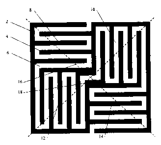
Figure 1 shows the preferred embodiment of claim I . Two conductive regions
are shown (2,4)
2 0 shaded different colours. The regions are spaced apart by a predetermined
distance (6). This
distance is normally determined by the minimum spacing rules set out in the
physical design
specification for the IC technology in use. The capacitance created between
the two
conductors is due to the lateral flux through the dielectric. The total
capacitance of the inter
digitized structure is made up primarily from the perimeter of the facing
edges of the two
2 5 conductive regions.
The overall capacitor structure of Figure 1 is made up of 4 separate regions.
Each region is
defined by the orientation of the inter-digitized fingers within said region.
The upper left
region (8) had fingers perpendicular to the upper right region (10). The lower
right region (14)
has fingers parallel to the upper left region (8). The lower left region (12)
is again
30 perpendicular to the upper left region (8) but parallel to the upper right
region (10). The entire
structure is symmetrical if miwored about both diagonal axes ( 16,18). In
other words, it is
identical if rotated 180 degrees. The overall structure has near symmetry in
the number of
fingers that are oriented in a given direction and the different orientations
are arranged in a
common centroid fashion about the center of the capacitor.
35 While the preferred embodiment shows 4 distinct regions to obtain an
overall equality in the
orientation of the inter-digitized fingers, it is understood that this
stnacture could be extended to
more regions, given a larger area. Each region would contain fingers which
originated from
lines extending from the center of the structure, as in the 4 region case of
Figure 1.
Figure 2 illustrates an example of claim 2, where two identical layers, like
that described in
4 0 claim 1 are present, one on top of another. The respective conductive
regions in the two layers
CA 02395900 2002-08-12
FILE N0. PRIVILEGED AND CONFIDENTIAL
- 6 -
are connected by vias (20). The vial are typical of those defined by the
physical design
specification in use. In this case the capacitor is still made up of primarily
lateral flux, as the
two different conductive regions in each layer do not overlap the unrelated
conductive region
in the next layer.
While the present embodiment shows the inter-layer connections using vias at
the outermost
conductors only, other embodiments could have the inter-layer connections
created differently.
For example, the region at the center of the structure (22) could be used for
via connections or
the via connections could be made throughout the structure providing that the
fingers are made
wide enough to allow for them. It is intended that these claims cover any of
these methods.
Figure 3 illustrates an example of claim 3, where the orientation of the
structure in the second
layer is rotated by 90 degrees. The conductors in the second layer (24,
outlined with a dashed
line) for each of the 4 regions described above are perpendicular to the
conductors in the first
layer. This has the effect of increasing the overall capacitance by using
vertical flux where the
conductive region in one layer coincides with the unrelated conductive region
in the next layer.
The vertical flux as well as the same lateral flux from the structure in
Figure 2 adds to give an
overall higher capacitance. While the higher capacitance density may be
desirable, the vertical
flux can suffer from more variation over different areas on the chip and from
one chip to
another, compared to the lateral flux [1 ].
Figure 4 illustrates the third conductive region (26) described in claim 6.
This conductive
2 0 region surrounds the entire structure, maintaining the same distance for
each outer edge. The
outer conductor serves to minimize the variation in the parasitic capacitances
at the edges of
the capacitor. With the third c<mductive region, the parastics at the outside
edges of the
capacitor will not depend on structures that are placed near to the capacitor.
This outside
conductor is extended to all the layers in which the capacitor is used, as in
claims 2 through 5.
2 5 This conductor may be electrically connected to a power signal or ground
signal or it may be
left as a floating node.
In all the examples described above, the resultant capacitor structure can be
used as an array,
where the structure described above is used as the unit section of the array.
By varying the
orientation of the cells in the array a uniform, well-matched capacitor array
can be created.
3 0 While the present invention has been illustrated and described with
reference to specific
embodiments, further modifications and improvements will occur to those
skilled in the art. It
is to be understood, therefore, that this invention is not limited to the
particular forms
illustrated, for example, other types of filters or tuning algorithms could be
used. It is intended
that these claims cover all modifications that do not depart from the spirit
and scope of this
3 5 invention.