Note: Descriptions are shown in the official language in which they were submitted.
CA 02396820 2002-07-08
WO 01/59479 PCT/SE01/00234
RADIATION DETECTOR, AN APPARATUS FOR USE IN RADIOGRAPHY AND A
METHOD FOR DETECTING IONIZING RADIATION
FIELD OF THE INVENTION
The invention relates to a detector for detection of ionizing
radiation, to an apparatus for use in radiography and to a
method for detecting ionizing radiation.
BACKGROUND OF THE INVENTION AND RELATED ART
A detector, an apparatus and a method of the kind mentioned
above are described in the copending Swedish application SE-
9901325-2, which is incorporated herein by reference. The
detector described therein includes a gaseous parallel plate
avalanche chamber. The detector provides good position
resolution, high X-ray detection efficiency, and the ability
to count every photon absorbed in the detector. This enables
numerous possibilities for processing the detection signals,
such as energy detection, discriminating detection signals
from photons in certain energy ranges or from photons incident
at certain distance ranges from the anode or the cathode.
US-5 614 722 discloses a radiation detector based on charge
amplification in a gaseous medium. Said detector includes a
substrate having a cavity defined therein, an anode surface
positioned in the bottom of the cavity and a cathode
positioned adjacent the cavity opening. A drift electrode is
juxtaposed over the substrate opposite the cavity and defines
a region containing a gaseous medium. Said document also
discloses that the cathode terminates in a cathode sidewall,
which preferably terminates short of the cavity opening, and
the cathode sidewall may terminate at greater distances from
CA 02396820 2002-07-08
WO 01/59479 2 PCT/SE01/00234
the cavity opening. Moreover, in said document it is mentioned
that the gaseous medium of the detector can be replaced with a
liquid such as, for example, liquid argon or liquid xenon.
A drawback with conventional gaseous parallel plate avalanche
chambers is that the electrical field between the electrodes,
i.e. the voltage applied between the electrodes, needed for
efficient operation of the instrument is close to the limit
where sparks are produced which could harm the detector.
SUMMARY OF THE INVENTION
A main object of the invention is to provide an improved
detector for detection of ionizing radiation, which employs
avalanche amplification, and ensures stronger focusing effect
than in conventional designs, and which can be manufactured in
a simple and cost effective way. The stronger focusing effect
will render the streamer formation more difficult compared to
prior art designs.
This and other objects are attained by a detector for
detection of ionizing radiation, comprising a chamber filled
with an ionizable medium, at least one first electrode
arrangement provided in said chamber and including an electron
avalanche amplification unit, which includes at least one
avalanche cathode and at least one avalanche anode between
which a voltage is to be applied for creation of an electric
field for avalanche amplification, at least one arrangement of
read-out elements for detection of electron avalanches, said
at least one avalanche cathode having at least one hole or
opening, wherein the area of said at least one hole or opening
in the avalanche cathode is lager than the area of at least
one associated anode, as seen from above, and wherein said at
CA 02396820 2002-07-08
WO 01/59479 3 PCT/SE01/00234
least one anode is centered with respect to said at least one
hole or opening in the avalanche cathode, characterized in
that at least one focusing electrode is arranged between said
at least one avalanche cathode and said at least one avalanche
anode and has an opening or hole the area of which is smaller
than the area of the at least one hole or opening in said
avalanche cathode but larger than the area of said at least
one avalanche anode.
The detector also can operate at high X-ray fluxes without
performance degradation and has a long lifetime.
The detector of claim 1 also achieves effective detection of
any kind of radiation, including electromagnetic radiation as
well as incident particles, including elementary particles.
It is also an object of the invention to provide an apparatus
for use in radiography comprising said detector for detection
of ionizing radiation, which employs avalanche amplification,
provides well-defined avalanches, and can be manufactured in a
simple and cost effective way.
This and other objects are attained by an apparatus for use in
radiography, comprising an X-ray source, and a detector for
detection of ionizing radiation, comprising a chamber filled
with an ionizable medium, at least one first electrode
arrangement provided in said chamber and including an electron
avalanche amplification unit, which includes at least one
avalanche cathode and at least one avalanche anode between
which a voltage is to be applied for creation of an electric
field for avalanche amplification, at least one arrangement of
read-out elements for detection of electron avalanches, said
CA 02396820 2002-07-08
WO 01/59479 4 PCT/SE01/00234
at least one avalanche cathode having at least one hole or
opening, wherein the area of said at least one hole or opening
in the avalanche cathode is lager than the area of at least
one associated anode, as seen from above, wherein said at
least one anode is centered with respect to said at least one
hole or opening in the avalanche cathode and wherein at least
one focusing electrode is arranged between said at least one
avalanche cathode and said at least one avalanche anode and
has an opening or hole the area of which is smaller than the
area of the at least one hole or opening in said avalanche
cathode but larger than the area of said at least one
avalanche anode.
The apparatus for use in radiography may also include a simple
and inexpensive detector that can operate with high X-ray de-
tection efficiency and with good energy resolution for X-rays.
The apparatus for use in radiography may also include a detec
tor which can operate at high X-ray fluxes without a perform
ance degradation and has a long lifetime.
It is also an object of the invention to provide a method for
detection of ionizing radiation, which employs avalanche
amplification, provides well-defined avalanches and focusing
of the electrons by means of at least one focusing electrode,
and can be implemented in a simple and cost effective way.
This and other obj ects are attained by a method for detecting
ionizing radiation, wherein the radiation interacts with atoms
in a volume filled with an ionizable medium, for creation of
released electrons, said method comprising the steps of:
CA 02396820 2002-07-08
WO 01/59479 5 PCT/SE01/00234
forming in each of at least one region, including at least one
avalanche cathode and at least one avalanche anode, a
concentrated electric field for causing electron avalanches,
detecting the electron avalanches with read-out elements,
focusing the electrons with at least one anode having a
smaller area than associated holes or openings in the at least
one avalanche cathode, wherein the area of the at least one
anode is centered with respect to the associated holes or
openings in the at least one cathode, subjecting the electrons
to a first electric field in a conversion and drift volume,
said first electric field forces the electrons to enter the at
least one region with a concentrated electric field,
c h a r a c t a r i z a d b y the further step of focusing
the electrons with at least one focusing electrode arranged
between the at least one avalanche cathode and the at least
one avalanche anode, said at least one focusing electrode
having a hole or opening, the area of which is smaller than
the area of the hole or opening in the at least one avalanche
cathode.
The method can be used at high X-ray fluxes.
BRIEF DESCRIPTION OF THE DRAWINGS
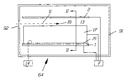
Figure 1 illustrates schematically, in an overall view, a
general embodiment of a detector for radiography.
Figure 2 is a schematic, partly enlarged, cross sectional
view, taken at II-II in Figure 1, of a detector according to a
first specific embodiment of the invention.
CA 02396820 2002-07-08
WO 01/59479 6 PCT/SE01/00234
Figure 3 is a schematic, partly enlarged, cross sectional
view, taken at II-II in Figure l, of a detector according to a
second specific embodiment of the invention.
Figure 4 is a schematic cross sectional view of an alternate
embodiment of an anode.
Figure 5 is a schematic, partly enlarged, cross sectional
view, taken at II-II in Figure l, of a detector according to a
third specific embodiment of the invention.
Figure 6 is a schematic, partly enlarged, cross sectional
view, taken at II-II in Figure 1, of a detector according to a
fourth specific embodiment of the invention.
DESCRIPTION OF PREFERRED EMBODIMENTS
Fig. 1 is a sectional view in a plane orthogonal to the plane
of a planar X-ray beam 9 of a detector 64 for radiography.
A major fraction of the incident X-ray photons are detected in
the detector 64, which includes a conversion and drift volume
13 and an electron avalanche amplification unit 17. The X-ray
photons may enter sideways between two electrode arrangements
l, 2, between which an electric field for the drift of
electrons and ions in the conversion and drift volume 13 is
created or alternatively enter the detector from any direction
in the range of 0-180° where 0° is defined as coinciding with
the above-mentioned sideways entry direction.
The detector 64 and its operation according to the invention
will be further described below.
CA 02396820 2002-07-08
WO 01/59479 ~ PCT/SE01/00234
The detector 64 includes a first drift electrode arrangement
being a cathode plate 2 and a second drift electrode
arrangement being an anode plate 1. The plates 1,2 may be
mutually parallel and a gap or region 13 between said plates
includes an ionizable medium, such as a gaseous medium, liquid
medium or a solid medium, and the plates enclose the
conversion and drift volume 13 and the electron avalanche
amplification unit 17. Alternatively, the plates 1,2 are non-
parallel.
A voltage is applied between the anode plate 1 and the cathode
plate 2, and one or several voltages is (are) applied on the
electron avalanche amplification unit 17. This results in a
drift field causing a drift of electrons and ions in the gap
13, and electron avalanche amplification fields in the
electron avalanche amplification unit 17. In connection with
the anode plate 1 is an arrangement 15 of read-out elements
for detection of electron avalanches. Preferably the
arrangement of read-out elements 15 also constitutes the anode
electrode. Alternatively, the arrangement of read-out elements
15 can be formed in connection with the cathode plate 2 or the
electron avalanche amplification unit 17. The arrangement of
read-out elements 15 can also be formed on the anode or
cathode plate separated from the anode or cathode electrode by
a dielectric layer or substrate. In this case, the anode or
cathode electrode should be semi-transparent to induced
pulses, e.g. the anode or cathode electrode should be formed
as strips or pads.
In case of X-rays incident sideways on the detector 64 between
the cathode plate 2 and the anode plate 1, the detector 64 can
easily be made with an interaction path long enough to allow a
major fraction of the incident X-ray photons to interact and
CA 02396820 2002-07-08
WO 01/59479 8 PCT/SE01/00234
be detected. A collimator may be used for this purpose and
should preferably be arranged so that the thin planar beam en-
ters the detector 64 close to the electron avalanche amplifi-
cation unit 17 and preferably parallel therewith.
The gaseous ionizable medium can be a mixture of for example
90% krypton and 10% carbon dioxide or a mixture of for example
80o xenon and 20o carbon dioxide. The gas can be under pres-
sure, preferably in a range 1 - 20 atm. Therefore, the detec-
for 64 includes a gas tight housing 91 with a slit entrance
window 92, through which the X-ray beam 9 enters the detector
64. The window 92 may be made of a material, which is trans-
parent for the radiation, e.g. Mylar~, or a thin aluminum
foil. Detecting sideways incident beams in a gaseous ava-
lanche chamber 64 is a particularly advantageous additional
effect of the invention. The slit entrance window 92 is ar-
ranged at another place on the housing 91 than indicated in
figure 1 when X-rays enter the detector from a direction which
is not sideways, i.e. ~ 0 or 180°, alternatively the housing 91
may be made of a material transparent to the X-rays.
The liquid ionizable medium may for instance be THE (Tri
Methyl Ethane) or TMP (Tri Methyl Pentane) or any liquid ioni-
zable media with similar properties.
The solid ionizable medium may for instance be a semi conduct-
ing material, for instance, silicon. When the ionizable medium
is solid the housing 91 can be excluded.
In operation, the incident X-rays 9 enter the detector 64 and
travel through the gas, liquid or solid ionizable medium in a
direction in the range of 0-180° as defined above. Each X-ray
photon produces a primary ionization electron-ion pair within
CA 02396820 2002-07-08
WO 01/59479 9 PCT/SE01/00234
the gas, liquid or solid ionizable medium as a result of in-
teraction with an atom in the medium. This production may be
caused by photoeffect, Compton-effect or Auger-effect. Each
primary electron 11 produced loses its kinetic energy through
interactions with new atoms, causing further production of
electron-ion pairs (secondary ionization electron-ion pairs).
Typically between a few hundred and a few thousand secondary
ionization electron-ion pairs are produced from a 20 keV X-ray
photon in this process. The secondary ionization electrons 16
(together with the primary ionization electron 11) will drift
towards the electron avalanche amplification unit 17 due to
the electric field in the conversion and drift volume 13. When
the electrons 11, 16 enter regions of focused field lines of
the electron avalanche amplification unit 17, they will un-
dergo avalanche amplification, which will be described further
below.
The movements of the avalanche electrons and ions induce sig-
nals in the arrangement 15 of read-out elements for the detec-
tion of electron avalanches. The signals are picked up in con-
nection with the electron avalanche amplification unit 17, the
cathode plate 2 or the anode plate 1, or a combination of two
or more of said locations. The signals are further amplified
and processed by readout circuitry 14 to obtain accurate meas-
urements of the X-ray photon interaction points, and option-
ally the X-ray photon energies.
Figure 2 shows a schematic, partly enlarged, cross sectional
view, taken at II-II in Figure 1, of a detector 64 according
to a first specific embodiment of the invention. As seen, the
cathode plate 2 includes a dielectric substrate 6 and a con-
ductive layer 5 acting as a cathode electrode. The anode 1 in-
cludes a dielectric substrate 3 and a conductive layer 4 act-
CA 02396820 2002-07-08
WO 01/59479 1 ~ PCT/SE01/00234
ing as an anode electrode. Between the gap 13 and the anode l,
the electron avalanche amplification unit 17 is arranged. The
electron avalanche amplification unit 17 includes an avalanche
amplification cathode 18 and a focusing electrode 19, sepa-
rated by a dielectric 24. The dielectric 24 could be a gas,
liquid or a solid substrate 24 carrying the cathode 18 and the
focusing electrode 19, as shown in Figure 2.
Between the cathode 18 and the focusing electrode 19 a voltage
is applied by a DC power supply 7 for creation of a very
strong focused electric field in an avalanche amplification
region 25. The avalanche amplification region 25 is formed in
a region between and around the edges of the avalanche cathode
18 which are facing each other, where a concentrated electric
f field occurs due to the applied voltages . The DC power supply
7 is also connected with the cathode electrode 5 and the anode
electrode 4 (19). The voltages applied are selected so that a
weaker electric field, drift field, is created over the gap
13. Electrons 11, 16 (primary and secondary electrons) re-
leased by interaction in the conversion and drift volume 13
will drift, due to the drift field, towards the electron ava-
lanche amplification unit 17. The electrons 11, 16 enter the
very strong avalanche amplification fields and are acceler-
ated. The accelerated electrons 11, 16 interact with other at-
oms in the region 25 causing further electron-ion pairs to be
produced. Those electron-ion pairs will also be accelerated in
the field, and will interact with new atoms, causing further
electron-ion pairs to be produced. This process continues dur
ing the travel of the electrons in the avalanche region 25 to
wards the anode 4 and an electron avalanche is formed.
The avalanche region 25 is formed by an opening or channel in
the cathode 18 and in the dielectric substrate 24, if present.
CA 02396820 2002-07-08
WO 01/59479 11 PCT/SE01/00234
The opening or channel can be of any shape for instance circu-
lar, square, triangular, rectangular, elliptical etc., when
viewed from above, or continuous, longitudinal extending be-
tween two edges of the substrate 24, if present, and the cat-
s bode 18. In the case the openings or channels are circular
when viewed from above, they may be arranged in rows, each row
of openings or channels including a plurality of circular
openings or channels. A plurality of longitudinal openings or
channels or rows of circular channels may be formed beside
each other, parallel with each other or with the incident X-
rays. Alternatively, the circular openings or channels can be
arranged in other patterns.
As an example, the longitudinal channels in the cathode 18 can
have a width in the range 0.01-1 mm. The longitudinal openings
or holes in the focusing electrode 19 are smaller than the as-
sociated longitudinal openings or holes in the cathode 18. The
dielectric 24 may have an inclined surface 26 with respect to
a normal to a surface of the avalanche cathode 18, the in-
clined surface 26 forming a limiting surface of a region for
avalanche amplification. The size of the area of the anode 4,
as seen from above, is smaller than the associated area of the
focusing electrode 19.
The difference in size of the holes or openings in the cathode
18, the focusing electrode 19 and the anode 4 ensure stronger
focusing effect compared to holes or openings of equal sizes.
If a streamer appears at high gains they will be self-
quenched. The reason for the self-quenching is the focused
field lines and the radial dependency of the field strength
seen from the avalanche region 25.
CA 02396820 2002-07-08
WO 01/59479 12 PCT/SE01/00234
Alternatively the conductive layers 5, 4 can be replaced by a
resistive carrier of e.g. silicon monoxide, conductive glass
or diamond, with the dielectric substrates 3, 6 being replaced
by a conductive layer.
An electric field is created between the anode electrodes 4
and the focusing electrode 19. This field could be a drift
field, i.e. a weaker field, or an avalanche amplification
field, i.e. a very strong electric field.
As an alternative, the electric field in the conversion and
drift gap 13 (volume) can be kept high enough to cause
electron avalanches, hence to be used in a pre-amplification
mode.
The distance between the cathode plate 2 and the electron
avalanche amplification unit 17 may be in the range of 0-10
mm, but preferably within the range of 100-5000 Vim. The
distance between the avalanche amplification cathode 18 and
the focusing electrode 19 may be in the range of 0-10 mm, but
preferably within the range of 50-500 Vim. The distance between
the focusing electrode 19 and the anode substrate 3 may be in
the range of 0-1 mm, but preferably within the range of 50-500
Vim.
Figure 3 shows a schematic, partly enlarged, cross sectional
view, taken at II-II in Figure l, of a detector 64 according
to a second specific embodiment of the invention. As seen, the
cathode plate 2 includes a dielectric substrate 6 and a con-
ductive layer 5 acting as a cathode electrode. The anode 1 in-
cludes a dielectric substrate 3 and an extended conductive
layer 4 acting as an anode electrode. The avalanche cathode 18
acts in this embodiment, as the avalanche amplification unit
CA 02396820 2002-07-08
WO 01/59479 13 PCT/SE01/00234
17, i.e. the distance in Figure 2 between the avalanche cath-
ode 18 and focusing electrode 19 is reduced to 0 in this em-
bodiment. Due to the shape of extended anode 4 more field
lines per unit area may be incident at the top of said anode
S compared to the inclined surface, thereby increasing the gain
of the detector 64 . The area of the extended anode 4 , as seen
from above, is smaller than the associated area of the hole or
opening in the avalanche cathode 18. It is noted that the top
portion of the anode 4 may be any shape (for example, flat
rounded or pointed) as long as the shape allows more field
lines per unit area to be incident at the top of the anode 4
as compared with the inclined surface.
In figure 4, another embodiment of the extended anode 4 ar-
ranged on the substrate 3 is shown. In this embodiment the ex-
tended anode 4 has a smooth shape, e.g. like a half ellipse.
The height of the extended anode could be as high as the dis-
tance between the substrate 3 and the focusing electrode 19 if
present or the avalanche cathode 18 in absence of said focus-
ing electrode 19.
Figure 5 shows a schematic, partly enlarged, cross sectional
view, taken at II-II in Figure 1, of a detector 64 according
to a third specific embodiment of the invention. The anode 1
includes a dielectric substrate 3 and an extended conductive
layer 4 acting as an anode electrode. The avalanche cathode 18
and the focusing electrode 19 act, in this embodiment, as the
avalanche amplification unit 17. The distance between the
cathode 2, including a dielectric substrate 6 and a conductive
layer 5, and the avalanche cathode 18 is reduced to 0 in the
embodiment as shown in figure 5, thereby eliminating the vol-
ume 13, i.e. the drift and conversion volume. In this embodi-
ment the incident X-rays will enter the detector 64 directly
CA 02396820 2002-07-08
WO 01/59479 14 PCT/SE01/00234
in the avalanche region 25 where the electrical field is very
high. Due to the shape of extended anode 4 more field lines
per unit area will be incident at the top of said anode com-
pared to the inclined surface, thereby increasing the position
resolution of the anode 4. The area of the extended anode 4,
as seen from above, is smaller than the associated area of the
hole or opening in the avalanche cathode 18 and the area of
the hole or opening in the focusing detector.
Figure 6 shows a schematic, partly enlarged, cross sectional
view, taken at II-II in Figure 1, of a detector according to a
fourth specific embodiment of the invention. The anode 1 in-
cludes a dielectric substrate 3 and an extended conductive
layer 4 acting as an anode electrode. As seen, the cathode
plate 2 includes a dielectric substrate 6 and a conductive
layer 5 acting as a cathode electrode. Between the gap 13 and
the anode 1 an electron avalanche amplification unit 17 is ar-
ranged. The avalanche cathode 18 and the focusing electrode 19
represent, in this embodiment, the avalanche amplification
unit 17. The voltages applied are selected so that a weaker
electric field, drift field, is created over the gap 13. Elec-
trons 11, 16 (primary and secondary electrons) released by in-
teraction in the conversion and drift volume 13 will drift,
due to the drift field, towards the avalanche amplification
unit 17. The electrons 11, 16 enter the very strong avalanche
amplification fields and are accelerated. The accelerated
electrons 11, 16 interact with other atoms in the region 25
causing further electron-ion pairs to be produced. Those pro-
duced electron-ion pairs will also be accelerated in the
field, and may interact with new atoms, causing further elec-
tron-ion pairs to be produced. This process continues during
the travel of the electrons in the avalanche region towards
the anode 4 and an electron avalanche is formed. In compari-
CA 02396820 2002-07-08
WO 01/59479 15 PCT/SE01/00234
son to figure 2, the distance between the focusing electrode
and the dielectric substrate 3 is reduced to 0 in the embodi-
ment as shown in f figure 6 . Due to the shape of extended anode
4, more field lines per unit area will be incident at the top
of said anode compared to the inclined surface, thereby in-
creasing the gain of the apparatus. The area of the extended
anode 4, as seen from above, is smaller than the associated
area of the hole or opening in the avalanche cathode 18 and
the area of the hole or opening in the focusing detector.
An apparatus comprising the inventive detector, as described
above, may also include an X-ray source, for irradiation of an
object to be imaged. The X-rays from the X-ray source are
transmitted through the object and enter the inventive
detector 64.
In general, for all embodiments, the volume of gas, liquid or
solid may be very small, which results in a fast removal of
ions, which leads to low or no accumulation of space charges.
This makes operation at high rate possible.
In general, for all embodiments, smaller distances lead to low
operating voltages, which results in low energy and a reduced
possibility for sparks, which is favorable for the electro
nics .
A streamer is a form of channel of plasma in which a spark can
form. The focusing of the field lines in the embodiments is
also favorable for suppressing streamer formations. This also
leads to a reduced risk of sparks.
Although the invention has been described in conjunction with
a number of preferred embodiments, it is to be understood that
CA 02396820 2002-07-08
WO 01/59479 16 PCT/SE01/00234
various modifications may still be made without departing from
the spirit and scope of the invention, as defined by the
appended claims. For example the voltages can be applied in
other ways as long as the described electrical fields are
created.