Note: Descriptions are shown in the official language in which they were submitted.
CA 02398301 2002-07-23
WO 01/67568 PCT/GBO1/00898
1
QUANTUM WELL INTERMIXING
Background to the Invention
The monolithic integration of several optoelectronics
devices in optoelectronics integrated circuits (OEICs) and
photonic integrated circuits (PICs) is of considerable
interest for the development of telecommunications systems.
Tn OEICs, optical devices such as lasers and
electronic devices such as transistors are integrated'on a
single chip for high speed operation since parasitic
reactance in the electrical connections can be minimized
from the closely packed devices.
PICs are a subset of OEICs with no electrical
components, in which only photons are involved in the
communication or connection between optoelectronics and/or
photonic devices. The driving forces fox PICs are to
improve the complexity of next-generation optical
communication links, networking architectures and switching
systems, such as in multiple channel wavelength division
multiplexing (WDM) and high speed time division
multiplexing (TDM) systems. In PICs, besides gaining from
the low cost, size reduction, and increased packaging
robustness, the main advantage is that all the
interconnections between the individual guided-wave
optoelectronics devices are precisely and permanently
aligned with respect to one another since the waveguides
are lithographically produced.
In the integration process, complex devices are built
up from components that are very different in functionality
such as light emitters, waveguides, modulators and
detectors. Each component needs different material
structures to achieve optimized performance. As a result,
the ability to modify the bandgap energy and the refractive
index of materials is important in order to realize OEICs
and PICs. A number of techniques have emerged for this
purpose, including growth and regrowth, selective area
CA 02398301 2002-07-23
WO 01/67568 PCT/GBO1/00898
2
epitaxy or growth on a patterned substrate and quantum well
intermixing (QWI).
Growth and regrowth is a complicated and expensive
technique which involves growing, etching and regrowing of
quantum viell (QW) layers at selected areas on bulk
material. These layer structures are overgrown with the
same upper cladding but a different active region. This
approach suffers from mismatches in the optical propagation
coefficient and mismatches in the dimensions of the
waveguide at the regrown interface. Tn addition, this
process gives low yield and low throughput, and therefore
adds cost to the final product.
Selective area growth utilizes differences in
epitaxial layer composition and thickness produced by
growth through a mask to achieve spatially selective
bandgap variation. Prior to epitaxy growth, the substrate
is patterned with a dielectric mask such as Si02, in which
slots with different widths are defined. The growth rate
in the open areas depends on the width of the opening and
the patterning of the mask. No growth can take place on
top of the dielectric cap. However, surface migration of
the species can take place for some distance across the
mask to the nearest opening. The advantage of this
approach is a reduction in the total number of processing
steps such that essentially optimum laser and modulator
multiple quantum well (MQW) sections can be accomplished in
a single epitaxial growth stage. This process works well
under a precisely controlled set of parameters but is
difficult to manipulate in a generic fashion. Tn addition,
this technique gives poor spatial resolution of around 100
~.m, and hence the passive section generally has a
relatively high loss.
QWI is based on the fact that a QW is an inherently
metastable system due to the large concentration gradient
of atomic species across the QWs and barriers interface.
Hence, this allows the modification of the bandgap of QW
structures in selected regions by intermixing the QWs with
CA 02398301 2002-07-23
WO 01/67568 PCT/GBO1/00898
3
the barriers to form alloy semiconductors. This technique
offers an effective post-growth method for the lateral
integration of different bandgaps, refractive index and
optical absorption within the same epitaxial layers.
The QWI technique has been gaining recognition and
popularity for which several potential applications in
integrated optoelectronics have been identified, for
example bandgap-tuned electroabsorption modulators,
bandgap-tuned lasers, low-loss waveguides for
interconnecting components on an OEIC or PIC, integrated
extended cavities for line-narrowed lasers, single-
frequency distributed Bragg reflector (DBR) lasers, mode-
locked lasers, non-absorbing mirrors, gain or phase
gratings for distributed feedback (DFB) lasers,
l5 superluminescent diodes, polarization insensitive QW
modulators and amplifiers and multiple wavelength lasers.
Current research has been focused on QWI using
approaches such as impurity free vacancy induced
disordering (IFVD), laser induced disordering (LID) and
impurity induced disordering (TID). Each of these QWI
techniques has its advantages and shortcomings.
The IFVD method involves the deposition of a
dielectric capping material on the QW materials and
subsequent high temperature annealing to promote the
generation of vacancies from the dielectric cap to the QW
materials and hence enhance the intermixing at selected
areas. For instance, in GaAs-AlGaAs QW materials, SiO~ is
known to induce out-diffusion of Ga atoms during annealing,
hence generating group III vacancies in the QW material.
The thermal stress at the interface between the GaAs and
the SiOa layer plays an important role. The thermal
expansion coefficient of GaAs is ten times larger than that
of SiO~. During high temperature annealing, the bonding in
the highly porous SiOz layer deposited using plasma-
enhanced chemical vapor deposition (PECVD) may be broken
due to the stress gradient between the GaAs and SiO~ film.
Thus, the out-diffusion of Ga helps to relieve the tensile
CA 02398301 2002-07-23
WO 01/67568 PCT/GBO1/00898
4
stress in the GaAs . These Ga vacancies then propagate down
to the QW and enhance the interdiffusion rate of Ga and Al,
and hence result in QWI. After the intermixing process,
the bandgap in the QW material widens and the refractive
index decreases.
The selectivity of this technique can be obtained
using an SrF~ layer to inhibit the outdiffusion of Ga,
hence suppress the QWI process. Using this technique,
devices such as multiple wavelength bandgap tuned lasers
and multiple channel waveguide photodetectors have been
successfully demonstrated.
Although IF~7D is a successful technique when employed
in GaAs/AlGaAs system, this technique gives poor
reproducibility in InGaAs/InGaAsP systems. Furthermore,
Z5 due to the poor thermal stability of InGaAs/InGaAsP
materials, the IFVD process, which requires high
temperature annealing, is found to give low bandgap
selectivity in InGaAs/InGaAsP based QW structures.
Laser induced disordering (LID) is a promising QWI
process to achieve disordering in InGaAs/InGaAsP QW
materials due to the poor thermal stability of the
materials. In the photoabsorption-induced disordering
(PAID) method, a continuous wave (CW) laser irradiation is
absorbed in the QW regions, thereby generating heat and
causing thermal induced intermixing. Although the
resulting material is of high optical and electrical
quality, the spatial selectivity of this technique is
limited by lateral flow to around 100 ~,m. A modification
of the PAID method, known as pulsed-PAID (P-PAID), uses
high-energy Q-switched Nd:YAG laser pulses to irradiate the
InP-based material. Absorption of the pulses results in
disruption to the lattice and an increase in the density of
point defects. These point defects subsequently
interdiffuse into the QW during high temperature annealing
and hence enhance the QW intermixing rate. Though P-PAID
can provide spatial resolution higher than 1.25 ~.m and
CA 02398301 2002-07-23
WO 01/67568 PCT/GBO1/00898
direct writing capability, the intermixed materials give
low quality due to the formation of extended defects.
Of all the QWI methods, impurity induced disordering
(IID) is the only process which requires the' introduction
5 of impurities into the QW materials in order to realize the
intermixing process. These impurities can be introduced
through focused ion beam, furnace-based impurity diffusion
and also ion implantation.
IID is a relatively simple and highly reproducible
intermixing process. It has the ability to provide high
spatial resolution for the integration of small dimension
devices and bandgap shifts can be controlled through the
implantation parameters. This technique is commonly used
to achieve lateral electrical and optical confinement in
semiconductors such that low threshold current and single
lateral-mode operation can be obtained. Furthermore, the
IID process is of considerable interest for the integration
of WDM systems, such as multiple wavelength laser sources,
low-loss waveguides, modulators and even detectors.
The IID effect is widely accepted to consist of two
stages. The first stage is to implant impurities into the
QW material. The subsequent stage is to anneal the
material to induce diffusion of both impurity and point
defects into the QWs and barriers, and hence interdiffusion
of matrix elements between QWs and barriers. In an
InGaAs/InGaAsP QW system, the interdiffusion of Group V
elements from barrier to well, which results in
blueshifting of the bandgap energy, are believed to be
caused by the diffusion of point defects generated during
the implantation process, the self-interdiffusion at
elevated temperature (thermal shift), and the diffusion of
the implanted species.
During implantation, impurities as well as point
defects, such as Group III vacancies and interstitials, are
introduced into the material in selected areas. The
diffusion of these point defects and impurities at elevated
temperature enhances the interdiffusion rate between the
CA 02398301 2002-07-23
WO 01/67568 PCT/GBO1/00898
6
QWs and barriers and hence promotes intermixing after
annealing. Under the influence of injected impurities, the
compositional profile of the QW is altered from a square to
a parabolic-like profile. As a result, after the
interdiffusion process, the local bandgap increases and the
corresponding refractive index decreases.
Using the IID technique, selective area intermixing
across a wafer can be obtained by using an Si02 implant
mask with various thicknesses. However, this technique
involves multiple lithography and etching steps which
complicate the fabrication process.
A paper entitled "Integration process for photonic
integrated circuits using plasma damage induced layer
intermixing", Electronics Letters, Volume 31, 449, 1995, by
B S Ooi, A C Bryce, and J H Marsh, describes a quantum well
intermixing process based on reactive ion bombardment
damage. In this technique, a high RF power, and hence high
damage, H~ plasma process was used to introduce point
defects on the surface of samples which were then annealed
to diffuse the point defects into the QW region. The
plasma exposure was performed using a parallel plate
reactive-ion etching (RIE) machine. Similarly, L M Lam et
al, in. a paper entitled "Plasma Immersion Ar+ Ion
Implantation Induced Disorder in Strained InGaAsP Multiple
Quantum Wells", Electronic Letters, Volume 34, No. 8, 16
April 1998, disclose a plasma immersion ion implantation
process that uses an RIE machine. In each of these
techniques, the QWI process is based on ion bombardment
damage and requires multiple cycles to affect fairly modest
degrees of bandgap shift.
The ability to control the bandgap across a III-V
semiconductor wafer is a key requirement for the
fabrication of monolithic PICs. The absorption band edge
of QW structures needs to be controlled spatially across a
wafer to allow the fabrication of integrated lasers,
modulators, and low-loss waveguides. Although QWI
techniques offer great advantages over growth and regrowth
CA 02398301 2002-07-23
WO 01/67568 PCT/GBO1/00898
7
and selective epitaxial growth techniques for the bandgap
engineering process, the spatial control of conventional
QWI techniques is indirect and complicated.
The explosive growth of Internet traffic, multimedia
services and high-speed data services has exerted pressure
on telecommunications carriers to expand the capacity of
their networks quickly and cost effectively. Carriers
normally have three options to expand capacity, ie install
new fibers, increase the bit rate of the transmission
system, or employ wavelength division multiplexing (WDM).
While the first option has problems of high cost and right
of-way and the second option has limited growth potential
because of inherent system limitations, the third option is
therefore very attractive because it is capable of manifold
increase of the network capacity at a modest cost.
Summary of the Iaveatioa
According to the. present invention, a method of
manufacturing a photonic integrated circuit comprising a
compound semiconductor structure having a quantum well
region, in which the method comprises the steps of
irradiating the structure using a source of photons to
generate defects, the photons having an energy (E) at least
that of the displacement energy (ED) of at least one
element of the compound semiconductor, and subsequently
annealing the structure to promote quantum well
intermixing.
The preferred radiation source is a plasma, although
there are a number of sources of high energy photons that
can be used. Suitable plasma sources include those
generated using an electron cyclotron resonance (ECR)
system, an inductively coupled plasma (ICP) system, a
plasma disk excited by a soft vacuum electron beam, and
plasma soft x-ray (SFR) devices. Other suitable sources of
high energy radiation include electrical gas discharge
devices, excimer lasers, synchrotron devices, flash x-ray
devices and gamma ray sources.
CA 02398301 2002-07-23
WO 01/67568 PCT/GBO1/00898
8
The method may include the step of masking a portion
of the structure to control the degree of radiation damage.
In this manner, the mask may be adapted to prevent
intermixing entirely. However, preferably the structure is
masked in a differential manner to selectively intermix the
structure in a spatially controlled manner by controlling
the exposure of portions of the structure in a
predetermined manner.
There are a number of suitable forms of exposure
l0 masks, including binary masks, phase masks, gray masks,
dielectric or metal masks, and photoresist masks. The
spatial control of intermixing is advantageously controlled
using a variable profile mask pattern. Our co-pending
International patent application number
(Agent s reference PJF01075W0)
describes a method for patterning a structure by exposing
a layer of photoresist through a gray scale mask. The
degree of quantum well intermixing is controlled in a
spatially selective manner in dependence on the optical
transmittance characteristics of the gray scale mask. This
technique is especially suitable for use in the present
invention since it allows a mask to be constructed that can
control the exposure of the structure to high energy
radiation. The photoresist mask pattern may be used alone
to control the degree of exposure or it may instead be used
to transfer a mask pattern to an underlying material, such
as a layer of dielectric material, through an etching
process.
The key feature of the present invention is the use of
a radiation source to cause radiation damage to a
crystalline structure. To achieve this, a well defined
minimum energy transfer is needed. This is called the
displacement energy, ED. Energy transfers exceeding ED will
cause atom displacement, either primary displacement, when
a host ion is struck by one of the instant particles, or
secondary displacement, when energy transfer is from the
host atom previously struck. Energy values of ED in eV for
CA 02398301 2002-07-23
WO 01/67568 PCT/GBO1/00898
9
a range of group TII-V materials are given in the table
below.
GaAs 9/9.4
InP 6.7/8.7
InAs 6.7/8.3
InSb 5.7/6.6
Whilst it is known that vacuum ultraviolet (VLTV)
radiation can cause damage to semiconductor structures,
this has always previously been investigated on the basis
that this damage should be avoided, or at least repaired by
annealing to ensure that these defects do not affect the
operation of the device.
This novel, low cost, and simple technique can be
applied for the fabrication of PICs in general, and WDM
sources in particular. By applying a QWI technique in
accordance with the present invention, the bandgap energy
of a QW material can be tuned to different degrees across
a wafer. This enables not only the integration of
monolithic multiple-wavelength lasers but further extends
to integrate with modulators and couplers on a single chip .
This technique can also be applied to ease the fabrication
and design process of superluminescent diodes (SLDs) by
expanding the gain spectrum to a maximum after epitaxial
growth.
The photonic integration research community currently
views QWI technology as a promising approach only for two
section photonic devices as conventional QWI processes
would otherwise become tedious and complicated. Although
it is complex and not cost effective, researchers have
instead preferred to use selective area epitaxy for
multiple-section integration. The present invention
demonstrates that the application of QWI is not limited to
two sectional devices. In addition, the technique is more
CA 02398301 2002-07-23
WO 01/67568 PCT/GBO1/00898
cost effective, and offers a higher throughput and higher
yield compared to selective area epitaxy.
Brief Description of the Drawings
5 Examples of the present invention will now be
described in detail with reference to the accompanying
drawings, in which:
Figure 1 is a schematic diagram of an example of an
ECR system;
10 Figure 2 is a schematic representation of an
InGaAs/InGaAsP SQW layer structure and a band diagram for
the structure;
Figures 3A and 3B are graphs illustrating the PL
spectra of samples exposed to Ar plasma;
Figure 4 is a graph illustrating the relationship
between Ar exposure time and relative bandgap energy shift
for different microwave powers;
Figure 5 is a graph illustrating the relationship
between process temperature and relative bandgap energy
shift;
Figure 6 is_a graph illustrating the relationship
between process pressure and relative bandgap energy shift;
Figure 7 is a schematic diagram of a sample partially
masked by a layer of photoresist;
Figure 8 is a graph illustrating the PL spectra
obtained from the sample of Figure 7 after exposure to an
Ar plasma;
Figure 9 is a graph illustrating the relationship
between RF power and relative bandgap energy shift;
Figure 10 is a graph illustrating the relationship
between microwave power and relative bandgap energy shift;
Figure 11 is a graph illustrating the relative bandgap
energy shift for samples exposed to Ar plasma with
different Si02 mask thicknesses;
Figure 12 is a schematic diagram of a broad area gain
guided laser; and,
CA 02398301 2002-07-23
WO 01/67568 PCT/GBO1/00898
11
Figure 13 is a graph illustrating the normalized
spectra of the device of Figure 12.
Detailed Descrip~ioa
The present invention is based on the discovery that
a more effective form of plasma induced QWI can be achieved
using high energy radiation, such as the Wv radiation
generated in an ECR generated plasma. This plasma process
operates in a totally different regime compared to that
described in earlier plasma induced disordering QWI
techniques. Tn an ECR, the microwave power control allows
for the generation of high energy radiation that is not
found in a conventional RIE machine. As a result, the QWT
blue shift obtained using high energy radiation is
significantly greater.
In an ECR system, a magnetic field is applied with an
exciting electromagnetic wave. Electrons under these
fields undergo a circular or orbital motion with a radius
relating to the strength of the fields, and rotating at a
frequency known as electron cyclotron frequency. If the
frequency of the electromagnetic wave is equal to the
cyclotron frequency, there will be a phase coherence
causing the electrons to continuously gain energy. Under
this condition, emission transfer of energy from the
exciting electromagnetic field to the electrons takes place
in what is known as the resonant process, In this resonant
process, the electrons in the bulk of the plasma gain their
energy from the exciting microwave and subsequently
transfer the energy to the molecules via collisions,
causing electron impact ionizations and generating a high
plasma density. The highly ionized ions emit photons with
line emissions.
ECR plasma is becoming increasingly popular in
microelectronics processing such as etching and thin film
deposition due to its ability to sustain highly dissociated
and highly ionized plasmas at relatively low pressures and
temperatures. It has the capability to operate at lower
CA 02398301 2002-07-23
WO 01/67568 PCT/GBO1/00898
12
pressure (typically 10-3 to 10-2 torr) than a conventional
RIE RF plasma and its degree of ionization can be as high
as 10% or so in some cases.
Resonance, or enhanced energy absorption, occurs when
the frequency of the alternating electric field equals the
cyclotron frequency. At this condition, the electron s
spiralvmotion is in phase with the alternating electric
field, allowing it to be accelerated resonantly with each
change in polarity. At the industrial microwave frequency
of 2.45 GHz, resonance occurs with a permanent magnet of
8736. For resonant absorption of energy to occur
efficiently, the electrons must undergo their cyclotron
orbits .'without collision with neutrals. Collisions
interfere with energy absorption due to energy transfer to
the neutrals and randomization of direction. As a general
rule, collisions result in inefficient electron cyclotron
heating at pressures above 20 mTorr. In an efficient ECR
discharge, ion and electron densities up to 1O12crri 3 are
achievable. This is roughly 100 to 1000 times the density
achievable in plasma generated by conventional RIE systems.
The ECR system used in the processing of the samples
described below was a Plasma Quest Series II PQM-9187-A
system. This is shown in Figure 1. The system 10 consists
of a microwave generator 11 of 2.45 GHz that is fed into
the ECR cavity Z2 through a quartz window. The microwave
power ranges from 0-1500 W. It is attached with a three-
stub tuner, which consists of three impedance matching
stubs installed within a 9-inch length of waveguide 13.
This is used to reduce the reflected power of microwave
energy directed to an easy-to-tune plasma source or
customer load. Additional Nd-Fe-B permanent magnets 14 of
alternating polarity are arranged around the perimeter of
the reactor and embedded in the grounded upper electrode.
This arrangement produces a magnetic field which better
confines the plasma. It focuses the plasma ions into the
center of the chamber, away from the chamber wall, and
thereby reduces the loss of charged species to the wall.
CA 02398301 2002-07-23
WO 01/67568 PCT/GBO1/00898
13
The ECR reactor also consists of a sample chuck 15
that is connected to a 13.56 MHz RF power supply 16. The
maximum power producible by the RF generator is 500 W. The
microwave power controls the amount of dissociation and
generation of reactive species. On the other hand, the RF
source provides the bias to the substrate and thus controls
the ion flux to the substrate, enhancing the directionality
of the process.
The InZGal_ZAs/InXGal_XAsxPl_Y structures used in the
examples described below were grown by metal organic
chemical vapour deposition (MOCVD) on an InP substrate.
The single quantum well (SQW) region is undoped and
consists of a 5.5 nm wide InZGa~_ZAs QW, with 12 nm InXGal_
xAsyPl_y (Ag=1. 26 ~,m) barriers . The active region was
bounded by step graded index (GRIN) InXGal_XAsYPl_y confining
layers. The thickness and composition of these layers were
50 nm of 2~g=1.18 ~,m, and 80 nm of Ag=1.05 ~,m, respectively.
The structure, which was lattice matched to InP throughout,
was completed with a 1.4 ~,m InP upper cladding layer and a
layer of 0.65 ~,m InXGal_XAsyPl_y followed by a 0.1 ~m InZGal_ZAs
which functions as the contact layer. The lower cladding
layer was sulfur-doped to a concentration of 2.5x10¹⁸etri 3.
The first upper cladding layer (InP) was doped with Zn to
a concentration of 7.4x101~crri 3 and the subsequent layer was
doped with 2x101gcrri 3 and 1. 3x1Ol9cm 3 concentration of Zn
respectively. A summary of the layer structure and
graphical interpretation is given in Table 1 and Figure 2,
respectively.
CA 02398301 2002-07-23
WO 01/67568 PCT/GBO1/00898
14
Table 1
Layer ThicknessMaterial Ts (g) DopantType Conc(cm~)
(nrii)
11 100 In(x)GaAs 6500.53 Zn p 8.000e+18
. 50 InGaAsP, ~,g=1.18650 Zn p 2.000e+18
5 9 ~ 1400 InP 650 Zn p 6.000e+17
8 80 InGaAsP, ~,g=1.05650 a
7 50 InGaAsP, ~,g=1.18650 a
6 12 aInGaAsP, 650 a
~,g=1.26
5 ~ . 5.5 In(x)GaAs 6500.53 a
10 4 12 TnGaAsP, ~,g=1.26650 a
3 50 InGaAsP, ~,~1.18650 S n S.OOOe+17
2 80 InGaAsP, ~,g=1.05650 S n S.OOOe+17
1 1000 InP 650 S n 2.000e+18
- - *InP Substrate
The GRIN structure is used to produce better optical
conf inement due to the di f f erence in ref ract ive index, i , a .
higher .refractive index in the QW as compared to the
barriers. The lower GRIN region is doped with S (n-type),
but the upper GRIN region (layer 7-8) is not doped with p-
type Zn to prevent it from diffusing into the QW region
during the QWI stage, hence degrading the quality of the
active layer. The top InGaAs layer is used as a contact
layer, and an InGaAsP.layer is sandwiched between the InP
and InGaAs layer so as not to cause an abrupt change from
InP structure to InGaAs structure.
Samples 17 were first cleaned and cleaved into size of
2x2 mm2. They were then exposed to Ar plasma within the
ECR arrangement 10 shown in Figure 1 at different process
conditions. For the first set of samples subjected to
plasma treatment, the RF and microwave powers were fixed at
450 W (self-DC bias around -35 V) and 1400 W respectively,
CA 02398301 2002-07-23
WO 01/67568 PCT/GBO1/00898
with an Ar flow rate of 50 sccm and process pressure of 30
mTorr. The exposure time was varied from 1 to 15 minutes.
Another set of samples was then exposed to the Ar plasma
with the same process conditions with the exception that
5 the microwave power was reduced to 800 W (self-DC bias
around -60 V). The exposure time was varied from 1 to 9
minutes. After plasma exposure, the samples were
subsequently annealed at 600°C for 2 minutes using a rapid
thermal processor (RTP). A GaAs proximity cap was used
10 during the annealing stage in order to provide As over
pressure to the samples.
Figures 3A and 3B show the PL spectra of the samples
exposed to Ar plasma at different times and microwave
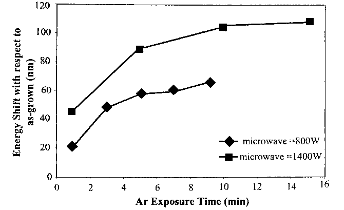
powers of 1400 W and 800 W, respectively. Figure 4 shows
15 the relative bandgap shift with respect to the as-grown
sample, as a function of exposure time, for Ar plasma
generated using RF 450 W and microwave powers of 800 W and
1400 W, respectively.
As can be seen from Figure 4, the QWI effect, which
causes the broadening of the bandgap energy and blue
shifting of the luminescence wavelength, can be observed
for the samples exposed to the Ar plasma. The degree of
intermixing increases gradually with increasing exposure
time for samples exposed at 1400 W. The bandgap shift
saturated at about 106 nm (72 meV) after 10 minutes of
plasma treatment. The saturation in energy shift implies
that the maximum point defects generated by both ion
bombardments and radiation damage saturates after an
exposure time of 10 minutes. The samples exposed to 800 W
produced results of similar trend to that of 1400 W, but
with lower degrees of blue shift. This could be attributed
to the use of lower microwave power, and hence lower
ionization of the Ar plasma. The highest attainable blue
shift under this exposure condition was found to be around
66 nm (42 meV) for the sample treated for 9 minutes.
As can be seen from Figure 5, there is no linear
relationship governing the bandgap energy shift and the
CA 02398301 2002-07-23
WO 01/67568 PCT/GBO1/00898
16
process temperature. A maximum bandgap shift of 32 nm was
obtained at a process temperature of 100°C. It is
generally expected that higher temperature would produce
higher degree of QWI under the ion bombardment damage
process. However, this phenomenon was not observed here.
It could thus be concluded that the concentration of the
damage induced by this process is below a certain threshold
to activate QWI.
Figure 6 shows the bandgap energy shift with respect
to different process pressures, The bandgap energy shift
increased to a maximum of 49 nm at process pressure of 30
mTorr and gradually decreases with increasing process
pressure.. From the results obtained, it could be explained
that as the process pressure increased from 10 mTorr to 30
mTorr, the density of the neutral and ionized species of
the plasma increased. Thus, a higher amount of damage is
produced, resulting in a higher degree of intermixing.
However, as the pressure continues to increase, the mean
free path of the ions becomes shorter. This causes the
amount of ions and neutral species colliding onto the
sample surface to reduce significantly, thus reducing the
amount of damage induced. Higher ionization due to
increasing process pressure should produce greater
radiation damage. However, the results indicate that the
radiation intensity change is minimal and its effect on QWI
over a range of different pressures remains fairly
constant.
QWT is generally only useful if it can be localized to
desired areas of the semiconductor, i.e. it is able to
intermix selectively. Selectivity is an important aspect
in a process as it provides the possibility of integration.
For QWI, interface sharpness between the intermixed and un
intermixed region is known as the spatial resolution. High
spatial resolution is necessary in intermixing processes as
it. ensures the compactness in device integration.
In order to study the selectivity of the plasma
process, samples 20 of 2 x 4 mm~ were prepared (Figure 7).
CA 02398301 2002-07-23
WO 01/67568 PCT/GBO1/00898
17
Half of the samples were then patterned with photoresist
21. These samples 20 were exposed to an Ar plasma of RF
450 W and microwave 1400 W for 5 minutes. The portion
masked with photoresist 21 is shielded from the damage
caused by the Ar plasma exposure and thus would undergo
none or minimal QWI after the RTP process.
Figure 8 shows the PL spectra obtained from the sample
20 after Ar exposure and subsequent thermal annealing. As
can be seen from the graph, the portion masked with a layer
of photoresist 21 underwent a small amount of bandgap shift
(~10 nm), whereas the portion 22 exposed to the plasma
exhibited a much larger bandgap shift of 64 nm, thus
producing a relative bandgap difference of 54 nm between
masked and unmasked regions. This result strongly
indicates that high selectivity is obtainable in the
InGaAs-InGaAsP samples using only photoresist as a masking
layer. The small amount of bandgap shift in the masked
region could be due to the bandgap modification induced by
thermal related effects.
The plasma generated using only RF power is expected
to predominantly create ion bombardment damage. This is
mainly due to the high potential difference between the
plasma and the semiconductor, which could be as high as 130
eV. By exposing the sample with such plasma, the QWI
mechanism in an ion-bombardment dominated plasma
environment can be investigated.
A set of samples was exposed to Ar plasma generated
using different RF conditions, while other process
parameters were held constant. All the exposures were
performed for 5 minutes. Figure 9 shows the relative
bandgap shift as a function of RF power. As can be seen
from Figure 9, samples treated with plasma under RF-only
conditions exhibit insignificant bandgap shift, with a
maximum shift of 22 nm (10 meV). The bandgap shifts under
different RF values were also rather small.
A further set of samples was then. exposed to plasma
generated by different microwave conditions, while other
CA 02398301 2002-07-23
WO 01/67568 PCT/GBO1/00898
18
process parameters were held constant. All the exposures
were performed for 5 minutes. Upon exposure, the samples
were annealed at 600°C for 2 minutes. Figure 10 shows the
relativelbandgap energy shift as a function of microwave
power.
As can be seen from Figure 10, samples treated with
plasma under microwave-only conditions produced a bandgap
energy shift as large as 66 nm (42 meV) . The amount of
bandgap shift also increases with increasing microwave
power. This result implies that high-energy VUV radiation
generated by high-density ECR plasma has a stronger
influence on the QWI effect than ion bombardment. It thus
plays an. important role in QWI in the TnGaAs-InGaAsP
structures using this process.
Table 2 below provides a summary of the process
variables investigated above, showing the potential
operating range of each variable and the preferred
operating~range.
Table 2
Potential Operating Preferred Operating
Range Range
RF power 0 ~ 500 W 0 W
Microwave power 300 ~ 3000 W 1000 ~ 2000 W
Process temperature25 ~ 500C 25 ~ 200 C
2 Process pressure 0.1 ~ 100 mTorr 20 ~ 50 mTorr
5
Exposure time 30 s ~ 1 hr 4 ~ 14 min
In the following example, a layer of Si02 is used to
act as an Ar plasma exposure mask to investigate the rate
of intermixing with respect to the SiO~ thickness deposited
on InGaAs/TnGaAsP MQW. The ability to control the amount
of intermixing with different Si02 thicknesses would enable
the lateral variation of bandgap energy in the sample.
This would enable the realization of devices requiring
CA 02398301 2002-07-23
WO 01/67568 PCT/GBO1/00898
19
different operating wavelengths across the sample, such as
multiple wavelength lasers.
InGaAs/InGaAsP MQW samples were cleaved into 2 x 2
mm2, and Si02 of different thicknesses were deposited on the
samples using a PECVD system. The SiOz thicknesses ranged
from 100 nm to 1200 nm. Four samples were used for each
Si02 thickness; this was done in order to study the
repeatability of the process.
All the samples were exposed to an Ar plasma of RF 450
W and microwave 1400 W for 10 minutes. After exposure, two
of the samples for each Si02 thickness were placed in a
solution of HF:H~O in the ratio of 2:1. This is to remove
the SiO~ layer on the samples before going through the
annealing process. Thus, the effect of annealing with and
without SiO~ capping could be studied. The samples were
then annealed in an RTP at a temperature of 590°C for 2
minutes. PL measurements were then performed to analyze
the degree of QWI.
Figure 11 shows the relative bandgap energy shift for
samples exposed to the Ar plasma with different SiO~
thicknesses. As can be seen from Figure 11, the degree of
intermixing decreased gradually as the thickness of SiO~
increases. However, the degree of intermixing remains
rather constant, having a bandgap shift in the range of 40
50 meV, when the SiOZ thickness is below 500 nm. No
significant bandgap shift was observed for an Si02 cap
thickness above 800 nm. In the SiOZ thickness range of
500-800 nm, the degree of intermixing reduced significantly
with increasing thickness.
Accordingly, we have shown that QWI in InGaAs/InGaAsP
MQW using Ar plasma exposure is controllable by altering
the thickness of SiO~ deposited on the sample before
exposure. The ability to control the degree of intermixing
enables the fabrication of devices which require different
bandgap energy across a sample. Devices such as multiple
wavelength lasers for WDM applications could be realized by
controlling the thickness of the Si02 across the wafer
CA 02398301 2002-07-23
WO 01/67568 PCT/GBO1/00898
before Ar exposure. With the invention of the novel gray
scale mask lithographic technique described in our co-
pending International patent application number
(Agent's reference PJF01075W0), this
5 fabrication would be further simplified, as it requires
only one-step RIE processing to transfer various thickness
of Si02 onto the samples. Alternatively, the mask may
consist only of a photoresist pattern having different
thicknesses applied using the same gray scale mask
10 technique.
In order to investigate the lacing wavelength of the
materials after QWI, broad area gain guided lasers were
fabricated from an as-grown sample (no plasma treatment and
annealing), a control sample (no plasma treatment but
15 annealed), and an Ar plasma intermixed sample:
Samples of 6 x 6 mm~ were cleaved along the crystal
orientation from an InGaAs/InGaAsP MQW wafer. They were
then exposed to Ar plasma of RF 450 W and microwave 800 W
for 5 minutes. An annealing step at 590°C for 120 seconds
20 was subsequently carried out to promote QWI. The samples
were then coated with a 200 nm PECVD SiO~ dielectric cap.
Next, 50 ~,m stripe windows were defined using
photolithography and both dry and wet etching were used to
open the windows. To minimize RIE damage from the CFQ and
OZ process, dry etching was first carried out for 5
minutes, followed by wet-etching using buffered HF for 10
seconds, to remove the remaining 75 nm of SiO~. These
lasers are gain-guided since the injected current produced
population inversion and a subtle waveguide effect only in
the 50 ~,m stripe regions. After this, front contact
metallization (p-type: Ti/Au, 50 nm/200 nm) was done using
an electron beam evaporator. Samples were then thinned to
a thickness of around 180 ~.m. Another metallization for
back contact (n-type: Au/Ge/Au/Ni/Au, 14 nm/14 nm/14 nm/11
nm/200 nm) were evaporated and the whole fabrication was
completed by annealing the samples using RTP at 360°C for
60 seconds. The processed samples were then scribed into
CA 02398301 2002-07-23
WO 01/67568 PCT/GBO1/00898
21
individual lasers with different cavity lengths for
characterization. A schematic diagram of a bandgap shifted
oxide stripe laser 30 is given in Figure 12.
Figure 13 shows the as-grown, control and Ar plasma
intermixed laser spectra. From the Figure, the control
samples and as-grown samples exhibit almost similar peak
lacing wavelength at 1.55 um, and the Ar plasma intermixed
lasers give a peak lacing wavelength at 1.517 ~,m, a shift
of 38 nm.