Note: Descriptions are shown in the official language in which they were submitted.
CA 02398613 2002-07-29
SF-806
1
Description
SUBSTRATE AND PROCESS FOR PRODUCING THE SAME
TECHNICAL FIELD
The present invention relates to a substrate having
inside an electrically conductive layer (internal
electrically conductive layer), having an electrically
conductive via hole formed between the internal
electrically conductive layer and the surface of the
substrate, which is formed from an aluminum nitride
sintering product, and relates to a process for producing
the substrate. More particularly, the invention relates
to the above-mentioned substrate which has high thermal
conductivity, good adhesion properties between the
aluminum nitride sintering product and the internal
electrically conductive layer or the electrically
conductive. via hole and high denseness of the internal
electrically conductive layer and the electrically
conductive via hole and hardly suffers warpage, and
relates to a process for producing the substrate.
BACKGROUND ART
Since aluminum nitride sintering products have
excellent properties such as high thermal conductivity,
CA 02398613 2002-07-29
SF-80b
2
good electrical insulation properties and a coefficient
of thermal expansion almost equal to that of Silicon (Si)
for forming integrated circuits, they are used as
substrates (sometimes referred to as "aluminum nitride
substrates" hereinafter) on which semiconductor circuit
parts are mounted. Particularly, aluminum nitride
substrates having a so-called electrically conductive aria
hole (sometimes referred to as a "via hole" simply
hereinafter) that is a through hole filled with an
electrically conductive material enable electrical
connection between external circuits of a semiconductor
through the via hole, and hence they are extremely useful.
In recent years, miniaturization of semiconductor
circuit manufactured articles and improvement of
performance thereof have been promoted, and with such
promotion, the number of the via holes formed in the
aluminum nitride substrates has been increased and the
arrangement of the via holes has been complicated. To
meet such market requirements, there has been utilized
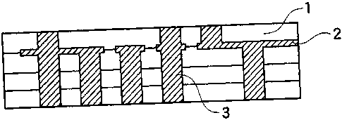
such an aluminum nitride substrate (1) as shown in the
sectional view of Fig. l, which has inside an internal
electrically conductive layer (2) and plural electrically
conductive via holes (3) which are electrically connected
to one another through the internal electrically
CA 02398613 2002-07-29
SF-806
3
conductive layer. The aluminum nitride substrate having
an electrically conductive layer inside can be produced
by laminating plural aluminum nitride molded products
having via holes through electrically conductive paste
S layers and then dewaxing and sintering the resulting
aluminum nitride molded product laminate.
The aluminum nitride sintering product produced by
the above process, however, has a thermal conductivity of
at most about 170 W/mK at 25°C because of restriction
imposed by that sintering of the electrically conductive
layer and sintering of the substrate are simultaneously
carried out.
On the other hand, as one method to calcine aluminum
nitride (simple substrate) having no via hole and no
conductive layer, a two-step firing method wherein the
sintering temperature is changed in the specific range is
carried out (Japanese Patent Laid-Open Publication No.
10552511993). In this method, a high thermal-conductive
aluminum nitride sintering product having a thermal
conductivity of about 200 W/mK at 25°C can be obtained.
When the sintered aluminum nitride substrate having
the via hole and the internal electrically conductive
layer is prepared according to the above-mentioned two-
step firing method, however, it was difficult to obtain
CA 02398613 2002-07-29
SF-806
4
sufficiently high adhesion strength between the aluminum
nitride sintering product and the internal electrically
conductive layer. Further, there was a problem that the
electrically conductive layer did not have satisfactory
denseness and as a result cracks occurred inside the
aluminum nitride substrate or the value of resistance of
the via hole was increased. Moreover, there was a
problem of large warpage of the substrate.
Accordingly, it has been desired to develop an
aluminum nitride substrate with a via hole and an
internal electrically conductive layer, which has a high
thermal conductivity of the aluminum nitride sintering
product, high adhesion strength of the internal
electrically conductive layer or the via hole to the
aluminum nitride sintering product and other excellent
properties.
DISCLOSURE OF THE INiJENTION
The present inventor has earnestly studied to solve
the above-mentioned problems. As a result, it has been
found that the defects of the substrate are caused by the
action of carbon after dewaxing, and it has been further
found the followings: cracks occurring inside the
aluminum nitride substrate and increase of warpage of the
CA 02398613 2002-07-29
SF-806
substrate can be inhibited by controlling the carbon
residue of the dewaxed aluminum nitride molded product
laminate to the specific range; the adhesion strength
between the aluminum nitride sintering product and the
5 internal electrically conductive layer or the via hole
can be sufficiently enhanced and stabled by controlling
the carbon residue of the dewaxed laminate, the
composition of the electrically conductive paste used and
the temperature range of the two-step firing method to
the specific ranges; and the thermal conductivity of the
aluminum nitride sintering product can also be
sufficiently enhanced by these operations. Based on the
finding, the present invention has been accomplished.
The substrate according to the invention is a
substrate having an internal electrically conductive
layer, at least one electrically conductive via hole
formed between the internal electrically conductive layer
and at least one surface of the substrate, which is
formed from an aluminum nitride sintering product,
wherein:
the thermal conductivity of the aluminum nitride
sintering product at 25°C is 190 W/mK or more, and the
adhesion strength between the aluminum nitride sintering
CA 02398613 2002-07-29
SF-806
6
product and the internal electrically conductive layer is
5.0 kg/mm2 or more.
In the substrate of the invention, the adhesion
strength between the aluminum nitride sintering product
and the electrically conductive via hole is preferably
5.0 kg/mm2 or more.
In the substrate of the invention, it is preferable
that the electrically conductive via hole comprises a
sintering product of an electrically conductive paste
having a refractory metal concentration of 85 to 95 o by
weight and the internal electrically conductive layer
comprises a sintering product of an electrically
conductive paste having a refractory metal concentration
of 65 to 83 °s by weight.
A metallized substrate according to the invention
has an electrically conductive pattern formed on at least
one surface of both surfaces of the above-mentioned
substrate, wherein at least a part of the electrically
conductive pattern is electrically connected to the
electrically conductive via hole.
The process for producing a substrate according to
the invention comprises:
forming at least one via hole-forming through hole
in a first aluminum nitride molded product comprising an
CA 02398613 2002-07-29
SF-806
7
aluminum nitride powder, a sintering aid and an organic
binder,
filling the through hole with an electrically
conductive paste (A) comprising 100 parts by weight of a
refractory metal powder and 2 to 10 parts by weight of an
aluminum nitride powder,
coating the surface of the first aluminum nitride
molded product with an electrically conductive paste (B)
comprising 100 parts by weight of a refractory metal
powder and 2 to 20 parts by weight of an aluminum nitride
powder to form an electrically conductive paste layer,
laminating a second aluminum nitride molded product
comprising an aluminum nitride powder, a sintering aid
and an organic binder on the first aluminum nitride
molded product through the layer of the electrically
conductive paste (B), and
dewaxing the resulting aluminum nitride molded
product laminate so that the carbon residue becomes 800
to 3000 ppm, then sintering the laminate at a temperature
of 1200 to 1700°C and further sintering the laminate at a
temperature of 1800 to 1950°C.
In the above process, it is preferable that the
concentration of the refractory metal in the electrically
conductive paste (A) with which the via hole-forming
CA 02398613 2002-07-29
SF-806
8
through hole of the first aluminum nitride molded product
is to be filled is in the range of 85 to 95 o by weight
and the concentration of the refractory metal in the
electrically conductive paste (B) with which the surface
of the first aluminum nitride molded product is to be
coated is in the range of 65 to 83 o by weight.
It is particularly preferable that the viscosity of
the electrically conductive paste (A) with which the via
hole-forming through hole of the first aluminum nitride
molded product is to be filled is in the range of 100 to
30000 poise at 25°C/5rpm and the viscosity of the
electrically conductive paste (B) with which the surface
of the first aluminum nitride molded product is to be
coated is in the range of 800 to 1200 poise at 25°C/5rpm.
According to the process of the invention, the
aforesaid substrate of the invention can be produced.
BRIEF DESCRIPTION OF THE DRAWINGS
Fig. 1 is a schematic sectional view of a substrate,
in a typical embodiment, according to the present
invention.
Figures 2 to 4 are schematic sectional views of
substrates, in other embodiments, according to the
present invention.
CA 02398613 2002-07-29
SF-806
9
Fig. 5 is a schematic perspective view of a
substrate, in another embodiment, according to the
present invention.
1: substrate
2: internal electrically conductive layer
3: electrically conductive via hole
BEST MODE FOR CARRYING OUT THE INVENTION
The substrate of the invention comprising an
aluminum nitride sintering product has an electrically
conductive layer formed inside. Although the thickness
of the internal electrically conductive layer is not
specifically restricted, it is usually in the range of 5
to 50 um. The material to constitute the internal
electrically conductive layer is not specifically
restricted provided that it is a refractory metal. The
material is usually a refractory metal such as tungsten
or molybdenum and is preferably one containing aluminum
nitride in an amount of 2 to 20 parts by weight based on
100 parts by weight of the refractory metal.
The internal electrically conductive layer is
usually formed as a flat film inside the substrate.
Although this layer is generally formed in parallel to
both surfaces of the substrate, it may be provided as a
CA 02398613 2002-07-29
SF-806
layer inclined to the substrate surface to a certain
extent when necessary.
The internal electrically conductive layer does not
need to be provided all over the horizontal section of
5 the aluminum nitride substrate, and it may be provided
partially. It is particularly preferable to form the
internal electrically conductive layer as a desired
circuit pattern according to the positions and the number
of the electrically conductive via holes to be formed.
10 The proportion of the internal electrically conductive
layer to the horizontal section of the aluminum nitride
substrate is desired to be in the range of usually 30 to
100 0.
In the present invention, two or more internal
electrically conductive layers may be provided at
prescribed intervals inside the aluminum nitride
sintering product. In this case, at least one via hole
is generally formed between the internal electrically
conductive layers to electrically connect those layers to
each other.
In the aluminum nitride substrate of the invention,
at least one via hole to link (electrically connect) the
internal electrically conductive layer to at least one
surface of the substrate is formed. The via hole may be
CA 02398613 2002-07-29
SF-806
11
formed between the internal electrically conductive layer
and one surface of the substrate or may be formed with
penetrating the upper and the lower surfaces of the
substrate through the internal electrically conductive
layer.
When plural via holes are formed in the substrate of
the invention, via holes corresponding to the pattern of
the internal electrically conductive layer are
electrically connected to one another through the
internal electrically conductive layer. Although the
number of via holes is not specifically restricted, the
proportion of the total volume of all the via holes to
the volume of the whole aluminum nitride sintering
product containing the via holes is preferably in the
range of 0.1 to 20 0.
Although the size of the via hole is not
specifically restricted, the diameter is preferably in
the range of 0.03 to 0.50 mm, and the ratio of the length
to the diameter (length/diameter) is preferably not more
than 4 0 .
The electrically conductive material filled in the
via hole is not specifically restricted provided that it
is a refractory metal. Usually, a high-melting point
such as tungsten or molybdenum is employed. The
CA 02398613 2002-07-29
SF-806
12
electrically conductive material is preferably one
containing aluminum nitride in an amount of 2 to 10 parts
by weight based on 100 parts by weight of the refractory
metal.
Typical embodiments of the substrate of the
invention having an internal electrically conductive
layer and a via hole formed therein are, far example,
those shown in the sectional views of Figs. 1 to 4.
The aluminum nitride substrate of the invention has
striking characteristics that the thermal conductivity of
the aluminum nitride sintering product is not less than
190 W/mK and the adhesion strength between the aluminum
nitride sintering product and the internal electrically
conductive layer is 5.0 kg/mm2 or more.
Since the aluminum nitride substrate of the
invention is of a so-called composite system containing a
via hole and an internal electrically conductive layer,
it is difficult to accurately evaluate the thermal
conductivity of the substrate itself in many cases. In
the present invention, therefore, a thermal conductivity
of an aluminum nitride substrate of the same thickness,
which is made of the same material by the same batchwize
dewaxing and sintering but has no via hole and no
internal electrically conductive layer, is employed as
CA 02398613 2002-07-29
~~-gQ~
I3
the thermal conductivity of the aluminum nitride
sintering product of the invention. If the thermal
conductivity of the aluminum nitride sintering product
portion can be directly measured using a residual portion
obtained by removing the internal electrically conductive
layer and the via hole from the aluminum nitride
sintering product by grinding or the like, it is a matter
of course to take the measured value as the thermal
conductivity. In the present invention, the thermal
U conductivity is a value measured at 25°C.
In the present invention, the adhesion strength
between the aluminum nitride sintering product and the
internal electrically conductive layer is measured in the
following manner. The surface of the substrate is ground
IS until the internal electrically conductive layer is
exposed outside, and on the thus exposed internal
electrically conductive layer, a thin film of Ti/Pt/.l~u is
formed. Then, the substrate is cut to give a chip of
about 5 mm x 5 mm. Onto the thin film of the chip, a pin
ZQ of 0.5 mm~J with a flat tip is soldered perpendicularly.
Then, the pin is pulled in the perpendicular direction to
measure a breaking strength. In this measurement,
whether the via hole underlies the internal electrically
conductive layer onto which the pin is to be soldered
CA 02398613 2002-07-29
SF-806
14
have little influence on the value of the adhesion
strength irrespective of the proportion of the underlying
via hole to the internal electrically conductive layer.
The above-mentioned measurement is carried out by
appropriately selecting the position of the pin at which
the internal electrically conductive layer is present all
over the lower surface of the pin to be soldered. If the
internal electrically conductive layer is formed by such
a fine circuit pattern that the measurement by the
selection of the above position is difficult, conversion
based on the area of the internal electrically conductive
layer actually evaluated has to be made.
It has been heretofore difficult to satisfy both of
increase of thermal conductivity of the aluminum nitride
sintering product and increase of adhesion strength
between the aluminum nitride sintering product and the
internal electrically conductive layer. In the substrate
of the invention, however, the thermal conductivity of
the aluminum nitride sintering product is 190 W/mK or
more and the adhesion strength between the aluminum
nitride sintering product and the internal electrically
conductive layer is 5.0 kg/mm2 or more, so that the
values of those properties are both high. Moreover, by
selecting the production conditions from more preferred
CA 02398613 2002-07-29
SF-806
ranges, a substrate wherein the thermal conductivity of
the aluminum nitride sintering product is 200 W/mK or
more and the adhesion strength is 7.0 kg/mmz or more,
particularly 10.0 kg/mm2 or more, can be obtained.
5 In the substrate according to the invention, the
adhesion strength between the aluminum nitride sintering
product and the electrically conductive via hole is
preferably 5.0 kg/mmz or more, more preferably 7.0 kg/mm2
or more, particularly preferably 10.0 kg/mm2 or more.
10 The adhesion strength between the aluminum nitride
sintering product and the electrically conductive via
hole stands for a breaking strength measured by cutting
the substrate across the center of the via-hole,
polishing the cut surface like a mirror surface, forming
15 a thin Ti/Pt/Au film on the cut surface, soldering a pin
of a diameter of 0.5 mm having a flat end in a manner to
come in contact with the surface of the via-hole
perpendicularly thereto, and pulling the pin from a
direction perpendicular thereto.
Next, the process for producing an aluminum nitride
substrate according to the invention is described. The
aluminum nitride substrate of the above structure may be
a substrate produced by any process, but it is preferably
obtained by a process comprising:
CA 02398613 2002-07-29
SF-806
16
forming at least one via hole-forming through hole
in a first aluminum nitride molded product comprising an
aluminum nitride powder, a sintering aid and an organic
binder,
filling the through hole with an electrically
conductive paste (A) comprising 100 parts by weight of a
refractory metal powder and 2 to 10 parts by weight of an
aluminum nitride powder,
coating the surface of the first aluminum nitride
molded product with an electrically conductive paste (B)
comprising 100 parts by weight of a refractory metal
powder and 2 to 20 parts by weight of an aluminum nitride
powder to form an electrically conductive paste layer,
laminating a second aluminum nitride molded product
comprising an aluminum nitride powder, a sintering aid
and an organic binder on the first aluminum nitride
molded product through the layer of the electrically
conductive paste (B), and
dewaxing the resulting aluminum nitride molded
product laminate so that the carbon residue becomes 800
to 3000 ppm, then sintering the laminate at a temperature
of 1200 to 1700°C and further sintering the laminate at a
temperature of 1800 to 1950°C.
CA 02398613 2002-07-29
SF-806
17
There is no specific limitation on the aluminum
nitride powder to constitute the first and the second
aluminum nitride molded products, and any of commonly
known ones is employable. In particular, a powder having
an average particle diameter, as measured by a
sedimentation method, of not more than 5 um is preferably
employed, and a powder having an average particle
diameter of not more than 3 um is more preferably
employed, and a powder having an average particle
diameter of 0.5 to 2 um is most preferably employed.
Further, an aluminum nitride powder having an average
particle diameter D1, as calculated using the specific
surface area, and an average particle diameter D2, as
measured by a sedimentation method, which satisfy the
following formulas is preferably employed, because such
an aluminum nitride powder can reduce a linear shrinkage
ratio in the firing process and thereby improve
dimensional stability of the sintering product or bring
the linear shrinkage ratio close to that of the internal
electrically conductive layer, whereby the adhesion
strength between the aluminum nitride sintering product
and the via hole or the internal conductive electrically
conductive layer can be further enhanced.
0 . 2 um ~ D 1 ~ 1 . 5 ~zm
CA 02398613 2002-07-29
SF-806
18
D2/D1 'c 2.60
Also preferable is an aluminum nitride powder which
has an oxygen content of not more than 3.0 o by weight
and a cation impurity content of not more than 0.5 % by
weight with the proviso that the composition of the
aluminum nitride is A1N, and particularly preferable is
an aluminum nitride powder having an oxygen content of
0.4 to 1.0 o by weight, a cation impurity content of not
more than 0.2 % by weight and a total amount of Fe, Ca,
Si and C among the cation impurities being not more than
0.17 o by weight. When such an aluminum nitride powder
is used, the thermal conductivity of the resulting
aluminum nitride sintering product is greatly improved,
so that such an aluminum nitride powder is preferably
used.
As the sintering aid added to the aluminum nitride
molded product in the present invention, commonly known
sintering aid can be used without any restriction.
Specifically, an alkaline earth metal compound, e.g., an
oxide such as calcium oxide, or a compound comprising
yttrium or a lanthanide element, e.g., an oxide such as
yttrium oxide, is preferably used.
Likewise, as the organic binder used for the
aluminum nitride molded product in the present invention,
CA 02398613 2002-07-29
SF-806
19
commonly known organic binders can be used without any
restriction. Examples of the organic binders include
acrylic resins, such as polyacrylic esters and
polymethacrylic esters: cellulose resins, such as methyl
cellulose, hydroxymethyl cellulose, nitrocellulose and
cellulose acetate butyrate; vinyl group-containing resins,
such as polyvinyl butyral, polyvinyl alcohol and
polyvinyl chloride; hydrocarbon resins, such as
polyolefins; and oxygen-containing resins, such as
polyethylene oxide. These resins are used singly or in
combination of two or more kinds. Of these, the acrylic
resins are preferably used because they have good
dewaxability and can reduce resistance of a via hole. As
other components such as a solvent, a dispersant and a
plasticizer, those commonly known can likewise be used
without any restriction.
As for the proportions of the components for
constituting the first and the second aluminum nitride
molded products, commonly known proportions can be
adopted without any restriction in the present invention.
For example, the sintering aid in an amount of 0.01 to 10
parts by weight and the organic binder in an amount of
0.1 to 30 parts by weight are preferably used based on
100 parts by weigh of aluminum nitride. Particularly,
CA 02398613 2002-07-29
SF-806
the sintering aid in an amount of 2 to 7 parts by weight
is preferably adopted since such amount is advantageous
in the enhancement of the thermal conductivity. Likewise,
there is no specific limitation on the process for
5 producing an aluminum nitride molded product using these
components, and in general, the molded product is formed
as a green sheet by a doctor blade method. The green
sheet may be used singly, or plural green sheets may be
laminated together to give a united one having a desired
10 thickness, prior to use.
In the present invention, each of the electrically
conductive pastes used for forming the via hole and the
internal electrically conductive layer contains the
aforesaid type of the refractory metal powder. As the
15 refractory metal powder for the electrically conductive
paste (A) for forming the via hole, a powder having an
average particle diameter, as measured by the Fischer's
method, of 1 to 2.5 um is preferably used, and a powder
having an average particle diameter of 1.6 to 2.0 um is
20 most preferably used, because occurrence of cracks inside
the via hole can be effectively inhibited. As the
refractory metal powder for the electrically conductive
paste (B) for forming the internal electrically
conductive layer, a powder having an average particle
CA 02398613 2002-07-29
sF-go6
21
diameter, as measured by the Fischer's method, of 0.8 to
5.0 um is preferably used, and a powder having an average
particle diameter of 1.0 to 3.0 um is most preferably
used, because a dense internal electrically conductive
layer is formed and occurrence of warpage of the aluminum
nitride substrate can be effectively reduced.
As the aluminum nitride powder used for the both
electrically conductive pastes, an aluminum nitride
powder commonly known can be used without any restriction.
Particularly, the aluminum nitride powder of the
aforesaid properties that is preferably used for the
aluminum nitride molded product is preferably used,
because not only it has good sintering properties with
the refractory metal powder and thereby exhibits an
effect to enhance adhesion properties of the internal
electrically conductive layer but also it reduces a
difference in the shrinkage ratio between the aluminum
nitride portion and the internal electrically conductive
layer portion to improve dimensional stability of the
sintering product.
In the present invention, the electrically
conductive paste (A) for forming the electrically
conductive via hole has a composition containing 2 to 10
parts by weight of the aluminum nitride powder based on
CA 02398613 2002-07-29
SF-806
22
100 parts by weight of the refractory metal powder. If
the amount of the aluminum nitride powder is less than 2
parts by weight in the electrically conductive paste, the
adhesion strength between the via hole and the aluminum
nitride sintering product becomes low or the difference
in the shrinkage ratio between the via hole portion and
the aluminum nitride sintering product portion is
increased to bring about a gap in the junction interface.
If the amount of the aluminum nitride powder is more
than 10 parts by weight, the viscosity of the
electrically conductive paste becomes high to deteriorate
filling properties of the paste, and as a result,
adhesion strength between the via hole and the aluminum
nitride sintering product is lowered by the voids
produced, or discoloration due to aluminum nitride is
liable to take place on the surface of the via hole to
increase the value of resistance. When the amount of the
aluminum nitride powder is in the range of 3 to 7 parts
by weight, the difference in the firing shrinkage ratio
between the via hole and the ceramic is extremely small,
so that the stress generated around the via hole is small
and the electrical resistance of the via hole can be
decreased. Hence, such amounts are preferable.
CA 02398613 2002-07-29
SF-806
23
On the other hand, the electrically conductive paste
(B) for forming the internal electrically conductive
layer has a composition containing 2 to 20 parts by
weight of the aluminum nitride powder based on 100 parts
S by weight of the refractory metal powder. If the amount
of the aluminum nitride powder is less than 2 parts by
weight in the electrically conductive paste, the adhesion
strength between the internal electrically conductive
layer and the aluminum nitride sintering product is
lowered, or the difference in the shrinkage ratio between
the aluminum nitride sintering product portion and the
internal electrically conductive layer portion is
increased to bring about separation on the junction
interface. If the amount of the aluminum nitride powder
is more than 20 parts by weight, the viscosity of the
electrically conductive paste becomes high to deteriorate
printability. On this account, printing non-uniformity
or blur takes place to lower adhesion strength between
the internal electrically conductive layer and the
aluminum nitride sintering product and to increase
electrical resistance of the internal electrically
conductive layer itself.
If the amount of the aluminum nitride powder is more
than 20 parts by weight, further, storage stability of
CA 02398613 2002-07-29
SF-806
24
the electrically conductive paste itself is decreased.
Therefore, if the electrically conductive paste is used
after a passage of several days from the preparation, the
viscosity of the electrically conductive paste becomes
high to deteriorate printability, and as a result,
adhesion strength between the internal electrically
conductive layer and the aluminum nitride sintering
product is lowered by the printing non-uniformity or blur
produced. In the electrically conductive paste for
forming the internal electrically conductive layer, the
amount of the aluminum nitride powder is in the range of
preferably 2 to 18 parts by weight, more preferably 11 to
18 parts by weight, from the viewpoint of storage
stability.
In addition to the refractory metal and the aluminum
nitride powder, to each of the electrically conductive
pastes used for forming the via hole and the internal
electrically conductive layer are generally added an
organic binder, an organic solvent, etc. to make them
pasty. Examples of the organic binders include acrylic
resins, such as polyacrylic esters and polymethacrylic
esters; cellulose resins, such as methyl cellulose, ethyl
cellulose, hydroxymethyl cellulose, nitrocellulose and
cellulose acetate butyrate; vinyl group-containing resins,
CA 02398613 2002-07-29
sF-go6
such as polyvinyl butyral, polyvinyl alcohol and
polyvinyl chloride; hydrocarbon resins, such as
polyolefins; and polyethylene oxide. Examples of the
organic solvents include di-n-butyl phthalate, diethylene
5 glycol mono-n-hexyl ether, 2-(2-butoxyethoxy)ethyl
acetate and terpineol.
In the electrically conductive paste (A) for forming
the via hole, the concentration of the refractory metal
is in the range of preferably 85 to 95 % by weight, more
10 preferably 87 to 93 % by weight, from the viewpoints of
enhancement of the adhesion strength of the via hole and
inhibition of occurrence of cracks inside the via hole.
In the electrically conductive paste (B) for forming the
internal electrically conductive layer, the concentration
15 of the refractory metal is in the range of preferably 65
to 83 % by weight, more preferably 72 to 83 % by weight,
from the viewpoint of obtaining higher adhesion strength
of the resulting electrically conductive layer to the
aluminum nitride sintering product.
20 The electrically conductive paste (A) for forming
the via hole is desirably prepared so as to have a
viscosity of preferably 100 to 30000 poise, more
preferably 500 to 7000 poise, at 25°C/5rpm, from the
viewpoints of enhancement of adhesion strength of the via
CA 02398613 2002-07-29
SF-806
26
hole and inhibition of occurrence of cracks inside the
via hole. The electrically conductive paste (B) for
forming the internal electrically conductive layer is
desirably prepared so as to have a viscosity of
preferably 800 to 1200 poise, more preferably 850 to 1000
poise, at 25°C/5rpm, from the viewpoint of obtaining
higher adhesion strength of the resulting electrically
conductive layer to the aluminum nitride sintering
product. In the preparation of these electrically
conductive pastes, other components commonly known, such
as a dispersant and a plasticizer, are used without any
restriction.
In the present invention, a through hole formed in
the first aluminum nitride molded product is filled with
the via hole-forming electrically conductive paste (A) to
obtain an aluminum nitride molded product having a via
hole-forming through hole filled with the paste (A).
There is no specific limitation on the method to form a
through hole in the aluminum nitride molded product, and
a method generally used, such as metal mold punching
method or a method of using a punching machine, is
employed. The diameter of the through hole is preferably
in the range of 0.05 to 0.50 mm in consideration of a
CA 02398613 2002-07-29
SF-806
27
desired hole diameter of a via hole formed in the
substrate.
For filling the through hole with the electrically
conductive paste (A), commonly known methods can be
adopted without any restriction. Specifically, a
printing method, the pressurized penetration method or
the like is used. When the ratio of the length to the
diameter (length/diameter) of the through hole is larger
than 2.5, the pressurized penetration method is
preferably used since the filling can be made more easily.
In the present invention, the surface of the first
aluminum nitride molded product having a through hole
filled with the electrically conductive paste is then
coated with the electrically conductive paste (B) for
forming the internal electrically conductive layer. For
the coating, commonly known methods are adopted without
any restriction. In general, coating by screen printing
is preferably used.
Subsequently, on the first aluminum nitride molded
product, a second aluminum nitride molded product that is
different from the first aluminum nitride molded product
is laminated with interposing the electrically conductive
paste layer formed as above. The second aluminum nitride
molded product comprises the same aluminum nitride powder,
CA 02398613 2002-07-29
SF-806
28
sintering aid and organic binder as previously described.
The second aluminum nitride molded product may be one
having a via hole-forming through hole or one having no
via hole-forming through hole. The through hole formed
in the second aluminum nitride molded product may not be
filled with no via hole-forming electrically conductive
paste. Also on the surface of the second aluminum
nitride molded product, the same layer of the
electrically conductive paste (B) as previously described
may be formed.
Further, three or more aluminum nitride molded
products may be laminated with interposing therebetween
the electrically conductive paste layers. Furthermore,
on one or both surfaces of the resulting aluminum nitride
molded product laminate, the electrically conductive
paste layer may be provided as a surface layer. The
structure of the aluminum nitride molded product laminate
is properly designed according to the structure of the
desired aluminum nitride substrate.
For laminating the aluminum nitride molded products,
commonly known methods are adopted without any
restriction. In general, the molded products are
preferably laminated and united by a hot pressing method
or a hot water isotropic pressure method.
CA 02398613 2002-07-29
SF-806
29
The aluminum nitride molded product laminate
obtained as above needs to be dewaxed so that the
aluminum nitride portion (aluminum nitride molded product
except via hole portion and internal electrically
conductive layer portion) has a carbon residue of 800 to
3000 ppm, preferably 1200 to 2500 ppm. If the carbon
residue is less than 800 ppm, the thermal conductivity of
the aluminum nitride sintering product becomes lower than
190 W/mK, and hence the object of the present invention
cannot be attained. If the carbon residue exceeds 3000
ppm, the sintering properties of the refractory metal
powder becomes bad, and therefore uniform and sufficient
adhesion strength between the aluminum nitride sintering
product and the via hole or the internal electrically
conductive layer cannot be obtained. In addition, cracks
take place in the aluminum nitride portion or warpage of
the aluminum nitride substrate becomes large, and hence
the object of the present invention cannot be attained.
In the dewaxing step, the dewaxing atmosphere is not
specifically restricted except an oxidizing atmosphere
such as the open air which is liable to oxidize the
refractory metal. For example, an atmosphere of an inert
gas such as nitrogen, argon or helium, an atmosphere of a
reducing gas such as hydrogen, an atmosphere of a mixed
CA 02398613 2002-07-29
SF-806
gas thereof, an atmosphere of a moistened gas thereof, or
vacuum is preferably employed.
The dewaxing temperature is appropriately selected
and is in the range of usually 500 to 1200°C, preferably
5 800 to 1000°C. Although the heating rate to attain this
temperature is not specifically restricted, it is
preferably not more than 10°C/min.
The dewaxing time is determined so that the carbon
residue of the molded product after dewaxing will be in
10 the range of 800 to 3000 ppm. Although the period of
time for which the dewaxing temperature is maintained
varies to some extent depending upon such condition as
the thickness of the molded product, density of the
molded product, proportions of the via hole and the
15 internal electrically conductive layer, dewaxing
temperature, etc., it is usually determined within the
range of 1 to 600 minutes.
The aluminum nitride molded product laminate having
been dewaxed as above (referred to as "dewaxed laminate"
20 hereinafter) is then sintering in a non-oxidizing
atmosphere or a dried reducing gas atmosphere. The non-
oxidizing atmosphere is, for example, an atmosphere of a
single gas such as nitrogen, argon or helium or a mixed
gas thereof, or a vacuum (or reduced pressure) atmosphere.
CA 02398613 2002-07-29
SF-806
31
The dried reducing gas atmosphere is, for example, an
atmosphere of hydrogen or a mixture of hydrogen and an
inert gas.
As for the temperature conditions in the firing, the
dewaxed laminate needs to be sintered at a temperature of
1200 to 1700°C, preferably 1500 to 1650°C, in the first
step, and then sintered at a temperature of 1800 to
1950°C, preferably 1820 to 1900°C, in the second step.
If the firing temperature in the first step is lower than
1200°C, reaction for removing oxygen in the aluminum
nitride by reduction with carbon remaining in the dewaxed
laminate hardly proceeds, and therefore the thermal
conductivity of the aluminum nitride sintering product
becomes lower than 190 W/mK. Consequently, the object of
the present invention cannot be attained. On the other
hand, if the firing temperature in the first step exceeds
1700°C, sintering of aluminum nitride proceeds before the
reaction for removing oxygen from the aluminum nitride by
reduction with carbon remaining in the dewaxed laminate
sufficiently proceeds, and as a result, oxygen is
diffused and dissolved in the aluminum nitride to inhibit
increase of thermal conductivity of the aluminum nitride
sintering product. Consequently, the object of the
present invention cannot be attained. When the firing
CA 02398613 2002-07-29
SF-806
32
temperature in the first step is in the range of 1500 to
1650°C, the reduction reaction to remove oxygen proceeds
effectively, so that this temperature range is preferable.
If the firing temperature in the second step is
lower than 1800°C, the aluminum nitride cannot be
sufficiently sintered, and therefore the thermal
conductivity of the aluminum nitride sintering product
becomes lower than 190 W/mK. Consequently, the object of
the present invention cannot be attained. If the firing
temperature in the second step exceeds 1950°C, not only
the adhesion strength between the via hole or the
internal electrically conductive layer and the substrate
is lowered but also warpage of the aluminum nitride
substrate becomes larger than 200 um. Consequently, the
object of the present invention cannot be attained.
Although the heating rate to attain this temperature is
not specifically restricted, it is preferably in the
range of 1 to 40°C/min.
The period of time for which the above temperature
is maintained is not specifically restricted, but it is
usually determined in the range of 30 minutes to 10 hours
in the first step and in the range of 1 minute to 20
hours in the second step. The firing in the first and
the second steps may be carried out as one-time sintering
CA 02398613 2002-07-29
SF-806
33
without decreasing the firing temperature, or may by
carried out as two-time sintering by decreasing the
firing temperature between the first step and the second
step. In consideration of the time and energy efficiency,
however, the sintering is preferably carried out as one-
time firing without decreasing the firing temperature.
When the distance between the upper or the lower
surface of the substrate and the internal electrically
conductive layer in the substrate to be produced by the
above process is prescribed, the substrate satisfying
such requirement can be obtained by, for example,
exposing the side end of the internal electrically
conductive layer outside on the side surface of the
substrate, then abrading or grinding the upper or the
lower surface of the substrate with measuring the
distance from the upper or the lower surface of the
substrate and stopping the abrading or grinding when the
prescribed distance is reached.
If warpage of the substrate having the internal
electrically conductive layer is large when the above
processing is carried out, the location of the internal
electrically conductive layer cannot be maintained
accurately. In an extreme case, the internal
electrically conductive layer is exposed outside on the
CA 02398613 2002-07-29
SF-806
34
substrate surface after the processing. The internal
electrically conductive layer exposed outside on the
substrate surface causes short circuit of the
electrically conductive pattern formed on the substrate
surface, and for this reason, the warpage is preferably
made as small as possible prior to the above processing.
The aluminum nitride substrate of the invention is
usually used for preparing a metallized substrate having
a structure wherein an electrically conductive pattern is
formed on at least one surface of the both surfaces
facing each other and at least a part of the electrically
conductive pattern is electrically connected to the via
hole. In this case, the electrically conductive pattern
may be formed on only one surface of the substrate, or
may be formed on both surfaces so that these surfaces are
electrically connected to each other by means of via
holes which connect the upper and the lower surfaces of
the substrate through the internal electrically
conductive layer.
The electrically conductive pattern in the invention
is not specifically restricted provided that it has
electrical conductivity, for example, a metallic thin
film or a thick film composed of a metal powder and an
inorganic or organic binder is usually used. Of such
CA 02398613 2002-07-29
SF-806
films, the metallic thin film is most preferably used
because of high electrical conductivity. As the metal to
constitute the metallic thin film, commonly known metals
are used without any restriction. Specifically, titanium
5 (Ti), chromium (Cr), molybdenum (Mo), tungsten (W),
aluminum (A1), tantalum (Ta), tungsten-titanium (W-Ti),
nickel-chromium (Ni-Cr) and tantalum nitride (Ta-N) are
preferably used because they have good adhesion to the
aluminum nitride sintering product.
10 The above metals may be used singly or in
combination of two or more kinds. The electrically
conductive pattern may be formed as a single layer or a
laminate of two or more layers.
In case of a laminate of two or more layers, it is
15 preferable to use the above-mentioned metals for the
first layer which is brought into contact with the
aluminum nitride sintering product since they have good
adhesion strength to the aluminum nitride sintering
product. Of those metals, Ti is more preferably used
20 since high adhesion strength can be stably obtained.
Although the thickness of the first layer used as an
adhesive layer is not specifically restricted, it is in
the range of usually 0.01 to 10 um, preferably 0.05 to 5
um, from the viewpoint of balance between guarantee of
CA 02398613 2002-07-29
SF-806
36
the reliability of adhesion strength due to increase of
the film thickness and economical effect due to
shortening of the film-forming time and reduction of the
materials accompanied by decrease of the film thickness.
For the second layer laminated on the first layer, a
commonly known metal can also be used. When the second
layer is an outermost layer in the electrically
conductive pattern of a two-layer laminate, at least one
of platinum (Pt), nickel (Ni), palladium (Pd), copper
(Cu), silver (Ag) and gold (Au) is preferably used
because of good electrical conductivity. Of these metals,
Pt, Pd, Ag or Au is more preferably used because of good
corrosion resistance.
When an electrically conductive pattern of a
laminate of three or more layers wherein a layer is
further laminated on the second layer is used as
described later, Pt, Ni, Pd, W, W-Ti or Mo having high
ability of diffusion inhibition is more preferably used
for the second layer in order to inhibit diffusion of
elements of the first and the third layer and thereby
ensure stable adhesion strength between the electrically
conductive pattern and the sintering product. Although
the thickness of the second layer is not specifically
restricted, it is in the range of usually 0.01 to 10 um,
CA 02398613 2002-07-29
SF-806
37
preferably 0.05 to 5 um because of similar reasons for
the first layer.
When the third layer is laminated on the second
layer, a commonly known metal is employable for the third
layer. For example, at least one of Pt, Ni, Pd, Cu, Ag
and Au is preferably used because of good electrical
conductivity. Of these metals, Pt, Pd, Ag or Au is more
preferably used because they have excellent corrosion
resistance. Although the thickness of the third layer is
not specifically restricted, it is in the range of
usually 0.05 to 10 um from the viewpoints of stability of
conductivity and balance between reliability and
economical effect.
In order to facilitate soldering of semiconductor
elements or the like onto the outermost metal layer, a
layer of at least one solder, such as a gold-tin (Au-Sn)
solder, a lead-tin (Pb-Sn) solder, a gold-silicon (Au-Si)
solder or a gold-germanium (Au-Ge) solder, may be
laminated or patterned. Further, a solder material
diffusion inhibition layer may be provided between the
outermost metal layer and the solder layer. For the
diffusion inhibition layer, Pt, Ni, Pd, W, W-Ti or Mo is
preferably used because of high ability of diffusion
inhibition.
CA 02398613 2002-07-29
SF-806
38
In order to maintain the prescribed value of
electrical resistance, a resistor thin film pattern to
electrically connect specific patterns of the
electrically conductive patterns to each other with the
prescribed value of resistance may be formed between the
specific patterns of the electrically conductive patterns.
The resistor thin film pattern is desired to have small
change in the value of resistance with time, and besides
it is desired that the value of resistance does not vary
even if the temperature of the metallized substrate is
changed.
The type of a resistor thin film used for the
resistor thin film pattern is not specifically restricted,
but preferably used is Ta-N, Ni-Cr of the like from the
viewpoint of the stability of the value of the resistance.
The composition of the alloy selected is preferably one
which causes small change in the value of resistance with
temperature. For example, a Ta2N layer is preferably used
as a layer of Ta-N type. Provided that the size of the
pattern is the same, the value of resistance becomes
smaller with decrease of the film thickness of the
resistor thin film. Therefore, the film thickness of the
resistor thin film is properly determined according to
the size of the desired pattern and the value of
CA 02398613 2002-07-29
SF-806
39
resistance. The film thickness thereof is usually in the
range of 0.01 to 0.5 um from the viewpoint of balance
between the stability of the value of resistance and the
economical effect.
In the electrically conductive pattern, an inductor
element and a capacitor element may be formed. The
inductor element can be formed by, for example, producing
a coil inductor pattern. The capacitor element can be
formed by, for example, laminating an insulating film
such as a film of tantalum pentoxide (Ta205) on the
electrically conductive pattern and then further
laminating an electrode film (upper electrode film) on
the insulating film.
The metallized substrate is usually produced by the
following process. That is, a large-sized substrate is
produced by the above process, then electrically
conductive patterns are formed repeatedly on the surface
of the substrate by the following method, and the
substrate is cut into a desired size to obtain plural
metallized substrates.
The size of the substrate is preferably large since
a great number of metallized substrates with electrically
conductive patterns can be formed at once. In general, a
CA 02398613 2002-07-29
SF-806
sintering product having a size of 1 to 4 inch square is
employed.
The substrate surface on which the electrically
conductive pattern is to be formed is preferably
5 subjected to grinding or polishing in order to enhance
the adhesion strength between the electrically conductive
pattern and the substrate. There is no specific
limitation on the grinding and the polishing, and any
technique commonly known is employed. In general,
10 lapping, polishing, barrel polishing, sand blasting,
abrasion using a grinder, or the like is employed. The
surface coarseness of the substrate varies depending upon
the purpose, but it is preferable to carry out the
polishing so that the centerline average coarseness (Ra)
15 becomes not more than 1.0 um, more preferably not more
than 0.1 um, because reliability of the soldering of the
semiconductor element is increased.
For forming the electrically conductive pattern,
commonly known methods can be used without any
20 restriction. Examples of the methods preferably used
include a sputtering method, a vaporization method, a
chemical vapor phase deposition method (CVD), an ion
plating method, a melt injection method, a screen
printing method, and a sol-gel coating method using spin
CA 02398613 2002-07-29
SF-806
41
coating or dip coating. For example, a metallic thin
film to form the electrically conductive pattern is
formed in the following manner in accordance with the
sputtering method. A target containing a component of
the metallic thin film is used, and the temperature of
the substrate is usually set in the range of room
temperature to 300°C. After the vacuum vessel is
evacuated to not more than 2x10⁻³ Pa, an argon gas is
introduced, then the vacuum vessel is maintained at a
pressure of 0.2 to 1.0 Pa, and the power of the RF (high-
frequency) electric source is set in the range of 0.2 to
3 kW to form the metallic film having a desired thickness.
For the formation of a thin film composed of a
nitride such as Ta-N that is used for the resistor thin
film pattern or a thin film composed of an oxide such as
Ta205 that is used for the capacitor pattern, a reactive
sputtering method is preferably employed. The reactive
sputtering method means a method in which a target
composed of a metallic component of the objective
compound is used, and a reaction gas containing another
component of the objective compound such as nitrogen or
oxygen is introduced into the vacuum tank together with
an electrical discharge gas to perform sputtering,
whereby a thin film is obtained. The composition of the
CA 02398613 2002-07-29
SF-806
42
resulting thin film is determined according to the ratio
between the electrical discharge gas and the reaction gas
introduced.
For example, a Ta-N film is formed in the following
manner in accordance with the reactive sputtering method.
A target of Ta is used, and the temperature of the
substrate is usually set in the range of room temperature
to 300°C. After the vacuum vessel is evacuated to not
more than 2X10⁻³ Pa, an argon gas as the electrical
IO discharge gas and a nitrogen gas as the reaction gas are
introduced, then the vacuum vessel is maintained at a
pressure of 0.2 to 1.0 Pa, and the power of the RF (high-
frequency) electric source is set in the range of 0.2 to
3 kW to form the metallic film having a desired thickness.
The shape of the electrically conductive pattern for
use in the invention can be arbitrarily selected
according to the use purpose, and can be made by
patterning a metallic thin film for constituting the
electrically conductive pattern. For the patterning, any
technique commonly known is adoptable according to the
use purpose of the substrate. Specifically, a metal
masking method, a wet etching method, a lift-off method,
a dry etching method or the like is adopted.
CA 02398613 2002-07-29
SF-806
43
In the patterning by the metal masking method, a
metal mask having a desired pattern previously formed is
fixed on the substrate, and the aforesaid sputtering or
vaporization is carried out to form an electrically
conductive pattern.
In the formation of the electrically conductive
pattern by the dry etching method, a desired pattern
using a photoresist or the like is formed on the metallic
thin film having been formed on the substrate by the
aforesaid sputtering or vaporization, then the
unnecessary portion of the metallic thin film is removed
by ion milling or the like, and then the resist is peeled
off.
The method to form an electrically conductive
pattern in which the circuit pattern contains a resistor
thin film pattern is not specifically restricted, and for
example, the following methods are available. In one
method, an electrically conductive pattern containing a
connecting portion to be connected with a resistor thin
film pattern is formed on the substrate first. Then, on
the electrically conductive pattern, a resistor thin film
for forming a resistor thin film pattern is laminated to
form a resistor thin film pattern. According to this
method, a circuit pattern in which the resistor thin film
CA 02398613 2002-07-29
SF-806
44
is laminated on the electrically conductive pattern at
the connecting portion can be obtained.
In another method, a resistor thin film pattern of a
shape containing a connecting portion is previously
formed on the substrate, and on the resistor thin film
pattern, an electrically conductive pattern is formed.
According to this method, a circuit pattern in which the
electrically conductive pattern is laminated on the
resistor thin film at the connecting portion can be
obtained. Further, the electrically conductive pattern
containing a resistor thin film pattern can be formed in
the following manner. That is, the resistor thin film
itself is used as the first layer that is brought into
contact with the substrate. On the resistor thin film, a
metallic thin film having an electrical resistivity lower
than that of the resistor thin film is laminated to form
an electrically conductive pattern, and the metallic thin
film formed on the resistor thin film is partially
removed between the specific patterns requiring the
prescribed value of resistance of the electrically
conductive pattern.
In order to suppress the change in the value of
resistance due to the lapse of time and temperature, the
resistor thin film pattern obtained as above is usually
CA 02398613 2002-07-29
SF-806
subjected to a treatment for stabilizing the value of
resistance (resistance stabilizing treatment) wherein an
oxide film is formed on the surface of the resistor thin
film. For the resistance stabilizing treatment, commonly
5 known technique can be used without any restriction. For
example, formation of an oxide film by an anodizing
method or formation of an oxide film by heating the
substrate having the resistor thin film pattern in the
open air is carried out to stabilize the value of
10 resistance. For adjusting the value of resistance of the
resulting resistor thin film pattern, commonly known
technique can be used without any restriction. For
example, laser trimming is available.
After the metallized substrate is plated with Ni, Au
15 or the like in order to improve solder wettability, an
electrode material such as a Si chip or pin can be
soldered or brazed onto the substrate. As the plating
means, electroless plating, electroplating, combination
thereof, and the like can be used without any restriction.
20 The substrate of the invention may be machined into
various shapes by, for example, conducting grooving such
as grinding or cutting. For example, the substrate may
be subjected to slitting and then cutting to give a
convex chip as shown in the perspective view of Fig. 5.
CA 02398613 2002-07-29
SF-806
46
This convex machined part is effectively used as a sub-
mount, a chip carrier or the like.
As understood from the above description, the
aluminum nitride substrate of the invention has a thermal
conductivity of 190 W/mK or more at 25°C, and has an
extremely high adhesion strength of 5.0 kg/mm2 or more
between the aluminum nitride sintering product and the
internal electrically conductive layer. Further, the
substrate has no cracks in the aluminum nitride sintering
d product and inside the via hole and hardly suffers
warpage. Accordingly, the substrate of the invention is
of extremely great value industrially.
If the aluminum nitride substrate of the invention
having the above properties is metallized to form a
~5 metallic thin film on the substrate surface, the
resulting metallized substrate can be favorably used for
electronic parts or semiconductor parts, such as a sub-
mount or a chip carrier of laser diode or light-emitting
diode, a heat sink and an IC package.
24
EXAMPLE
The present invention is further described with
reference to the following examples, but it should be
CA 02398613 2002-07-29
SF-806
47
construed that the invention is in no way limited to
those examples.
In the examples, various properties were measured by
the following methods.
(1) Carbon residue in aluminum nitride molded product
The carbon residue was analyzed by a non-difusion
type infrared ray-absorption carbon analyzer (EMIA-110,
manufactured by Horiba Seisakusho K.K.).
(2) Average particle diameter of aluminum nitride powder
The average particle diameter D1 based on the
specific surface area was calculated from the following
formula.
Dl (gym) - 6/(Sx3.26)
S: specific surface area of AlN powder (m2/g)
The average particle diameter D2 based on the
sedimentation method was measured by a centrifugal
particle size distribution-measuring device CAPA5000
manufactured by Horiba Seisakusho K.K.
(3) Evaluation of appearance of aluminum nitride
substrate
The appearance was observed visually and by a
stereomicroscope (x40), followed by evaluation.
A substrate in which no crack and no separation took
place on the interface between the aluminum nitride
CA 02398613 2002-07-29
SF-806
48
sintering product and the internal electrically
conductive layer, and no crack took place inside the
aluminum nitride sintering product, and no crack took
place in the internal electrically conductive layer was
evaluated as good, and a substrate in which at least one
of these defects took place was evaluated as bad.
(4) Warpage of aluminum nitride substrate
The warpage was measured by a surface roughness and
profile measuring device manufactured by Tokyo Seimitsu
K. K.
(5) Thermal conductivity of aluminum nitride sintering
product
An aluminum nitride substrate of the same thickness,
which was.prepared from the same materials by the same
batchwise dewaxing and sintered but had no via hole and
no internal electrically conductive layer, was measured
on the thermal conductivity by a laser flash method.
(6) Adhesion strength between internal electrically
conductive layer and aluminum nitride sintering product
The aluminum nitride substrate was polished like a
mirror surface until the internal electrically conductive
layer was exposed outside. Then, on the mirror surface
of the substrate, sputtering operations of Ti of 0.06 um,
Pt of 0.2 um and Au of 0.6 um were carried out in this
CA 02398613 2002-07-29
SF-806
49
order to form a metallic thin film under the high vacuum
of 10-3 Torr. The substrate was then cut to give a chip
of about 5 mm x 5 mm. On the treated surface of the chip,
a solder preform was placed, and on a hot plate at 230°C,
a Ni-plated pin was perpendicularly soldered onto the
surface of the substrate. The pin has a flat tip, has a
diameter of 0.5 mm and is made of 42-alloy. The solder
has a composition consisting of 60 o by weight of tin and
40 o by weight of lead.
After soldering of the pin, the substrate was set in
Strograph M2 manufactured by Toyo Seiki Seisakusho K.K.,
and the pin was pulled in the perpendicular direction to
measure a breaking strength. The rate of pulling was 10
mm/min. The position of the peel interface (peeling
mode) was checked by observing the pin and the broken
surface of the sintering product after the test by the
use of a stereomicroscope (X40), a metallized microscope
(x400) and an X-ray microanalyzer.
(7) Adhesion strength between electrically conductive via
hole and aluminum nitride sintering product
The substrate was cut across the center of the via
hole of the aluminum nitride sintering product, then the
cut surface was polished like a mirror surface, and on
the cut surface, a thin film of Ti/Pt/Au was formed.
CA 02398613 2002-07-29
SF-806
Then, a Ni-plated pin was perpendicularly soldered so
that the pin was brought into contact with the via hole
surface. The pin has a flat tip, has a diameter of 0.5
mm and is made of 42-alloy. The solder has a composition
5 consisting of 60 % by weight of tin and 40 o by weight of
lead. The substrate was set in Strograph M2 manufactured
by Toyo Seiki Seisakusho K.K., and the pin was pulled in
the perpendicular direction to measure a breaking
strength. The rate of pulling was 10 mm/min. The
10 position of peel interface (peeling mode) was checked by
observing the pin and the broken surface of the sintering
product after the test by the use of a stereomicroscope
(X40), a metallized microscope (X400) and an X-ray
microanalyzer.
15 (8) Electrical resistance of via hole
The aluminum nitride substrate was ground to remove
a portion above or below the internal electrically
conductive layer to allow the substrate to have a mirror
surface. The substrate was then divided into small chips,
20 and an electrical resistance of the via hole in each chip
was measured.
(9) Electrical resistance between electrically conductive
pattern and via hole
CA 02398613 2002-07-29
SF-806
51
Needle-like probes were brought into contact with
the electrically conductive pattern on each surface of
the metallized substrate, said electrically conductive
pattern being located right above the via hole
penetrating the substrate. Then, an electrical
resistance of the via hole of the metallized substrate
was measured by a four-terminal method.
(10) Appearance of metallized substrate
The appearance of the metallized substrate was
observed visually and by a stereomicroscope (X40),
followed by evaluation.
Whether disconnection of the electrically conductive
pattern due to cracks of the via hole or cracks of the
aluminum nitride sintering product had taken place or not
was checked. A substrate having no disconnection was
evaluated as good, and a substrate having even one
disconnection was evaluated as bad.
Example 1
100 Parts by weight of an aluminum nitride powder
(average particle diameter based on the sedimentation
method: 1.50 um, specific surface area: 2.50 m2/g,
average particle diameter calculated from the specific
surface area: 0.74 um, oxygen content: 0.80 0) having a
CA 02398613 2002-07-29
SF-806
52
composition shown in Table 1, 5 parts by weight of
yttoria, 2 parts by weight of n-butyl methacrylate as a
dispersant, 11 parts by weight of polybutyl acrylate as
an organic binder, 7 parts by weight of dioctyl phthalate
as a plasticizer and 50 parts by weight of a mixed
solvent of toluene and isopropyl alcohol were weighed,
and they were introduced into a ball milling pot,
followed by sufficiently mixing by the use of a nylon
ball.
CA 02398613 2002-07-29
SF-806
53
Table l:Analytic value of AIN powder
A1N content 97.9%
Element Content
Ca 105 ppm
Si 63 ppm
Fe 12 ppm
Ti 16 ppm
V 0.8 ppm
0 0.800
C 0.030
The resulting slurry was introduced into a def naming
apparatus so as to have a viscosity of 20000 cps, and
using the slurry, a sheet was formed on a polypropylene
film by a doctor blade type sheet-forming machine to
prepare an aluminum nitride green sheet having a
thickness of about 0.40 mm.
The aluminum nitride green sheet was cut into a size
of 65 x 65 mm. Then, three of the aluminum nitride green
sheets were laminated together to prepare an aluminum
nitride molded product (I). The laminating pressure was
50 kgf/cmz, the laminating temperature was 80°C, and the
laminating time was 15 minutes.
Then, the aluminum nitride molded product (I)
(65X65mm) was punched by a punching metal mold having a
diameter of 0.28 mm maintaining a pitch of 0.5 mm in
CA 02398613 2002-07-29
SF-806
54
order to form through holes arranged in a number of 120
120. Separately, to 100 parts by weight of a tungsten
powder (average particle diameter based on the Fischer's
method: 1.8 um) were added 5 parts by weight of the
aluminum nitride powder, 1.5 parts by weight of ethyl
cellulose as an organic binder, 5.0 parts by weight of 2-
(2-butoxyethoxy)ethyl acetate as a solvent and some
amounts of a plasticizer and a dispersant, and they were
sufficiently kneaded by means of an automatic mortar and
then a roll mill having three rolls to obtain a paste
(paste (A) for forming electrically conductive via hole)
having a viscosity of 2300 poise at 25°C/5rpm. The
concentration of the refractory metal in the paste (A)
was 90.8 % by weight. The paste (A) was filled in the
through holes of the aluminum nitride molded product (I)
by the pressurized penetration method. The filling
pressure was 50 psi, and the filling time was 120 seconds.
Then,_to 100 parts by weight of a tungsten powder
(average particle diameter based on the Fischer's method:
2.5 um) were added 5 parts by weight of the aluminum
nitride powder, 2 parts by weight of ethyl cellulose, 20
parts by weight of terpineol and some amounts of a
plasticizer and a dispersant, and they were sufficiently
kneaded by means of a grinding mill and then a roll mill
CA 02398613 2002-07-29
SF-806
having three rolls to obtain a paste (paste (B) for
forming internal electrically conductive layer) having a
viscosity of 950 poise at 25°C/5rpm. The concentration
of the refractory metal in the paste (B) was 79.5 % by
5 weight. The paste (B) was printed on one surface of the
aluminum nitride molded product (I) by screen printing to
form a whole surface solid pattern, whereby an
electrically conductive paste layer was formed on one
surface of the aluminum nitride molded product (I).
10 After drying, the thickness of the electrically
conductive layer was measured by a depth indicator, and
as a result, the thickness was 20 um.
Another aluminum nitride green sheet (II) cut into
65x65mm was punched by a punching metal mold having a
15 diameter of 0.28 mm maintaining a pitch of 1.5 mm in
order to form through holes arranged in a number of 40 X
40. The through holes were filled with the paste (A) by
the pressurized penetration method to prepare an aluminum
nitride molded product (II). The filling pressure was
20 650 psi, and the filling time was 180 seconds.
Then, the aluminum nitride molded product (II) was
laminated on the electrically conductive paste layer side
surface of the aluminum nitride molded product (I). The
laminating pressure was 80 kgf/cm2, the laminating
CA 02398613 2002-07-29
sF-go6
56
temperature was 80°C, and the laminating time was 15
minutes.
The resulting aluminum nitride molded product
laminate (i) having via hole-forming through holes filled
with the paste (A) and inside an electrically conductive
paste layer was dewaxed under heating at 900°C for 2
hours with passing a dry nitrogen gas at a rate of 30
1/min. The temperature was elevated at a rate of
2.5°C/min. A test sample having been dewaxed under
heating at the same time was examined on the carbon
residue, and as a result, the carbon residue was 2430 ppm.
After dewaxing, the dewaxed laminate was placed in an
aluminum nitride container, heated at 1580°C for 6 hours
in a nitrogen atmosphere (first step firing) and then
heated at 1870°C for 10 hours in a nitrogen atmosphere
(second step firing). Thus, an aluminum nitride
substrate having a thickness of 1.2 mm and a structure
shown in the sectional view of Fig. 1 was prepared.
Various properties of the aluminum nitride substrate
obtained were measured. The results are set forth in
Table 3.
Examples 2 and 3, Comparative Examples 1 and 2
CA 02398613 2002-07-29
SF-806
57
An aluminum nitride substrate was prepared in the
same manner as in Example 1, except that the composition
of the paste (A) (electrically conductive paste for
forming via hole) was changed as shown in Table 2.
Various properties of the aluminum nitride substrate were
measured. The results are set forth in Table 3.
Examples 4 and 5, Comparative Example 3
An aluminum nitride substrate was prepared in the
same manner as in Example 1, except that the composition
of the paste (B) (electrically conductive paste for
forming internal electrically conductive layer) was
changed as shown in Table 2. Various properties of the
aluminum nitride substrate were measured. The results
are set forth in Table 3.
Example 6
The aluminum nitride molded product laminate (i)
prepared in Example 1 was dewaxed under heating at 850°C
for 2 hours with passing a dry hydrogen gas at a rate of
12 1/min. The temperature was elevated at a rate of
2.5°C/min. A test sample having been dewaxed under
heating at the same time was examined on the carbon
residue, and as a result, the carbon residue was 900 ppm.
CA 02398613 2002-07-29
SF-80b
58
After dewaxing, the dewaxed laminate was sintered in the
same manner as in Example 1 to prepare an aluminum
nitride substrate. Various properties of the aluminum
nitride substrate were measured. The results are set
forth in Table 3.
Example 7
The aluminum nitride molded product laminate (i)
prepared in Example 1 was dewaxed under heating at 900°C
for 2 hours with passing a dry nitrogen gas at a rate of
1/min. The temperature was elevated at a rate of
2.5°C/min. A test sample having been dewaxed under
heating at the same time was examined on the carbon
residue, and as a result, the~carbon residue was 2800 ppm.
15 After dewaxing, the dewaxed laminate was sintered in the
same manner as in Example 1 to prepare an aluminum
nitride substrate. Various properties of the aluminum
nitride substrate were measured. The results are set
forth in Table 3.
Comparative Example 4
The aluminum nitride molded product laminate (i)
prepared in Example 1 was dewaxed under heating at 850°C
for 2 hours with passing a moistened hydrogen gas at a
CA 02398613 2002-07-29
SF-806
59
rate of 10 1/min. The temperature was elevated at a rate
of 2.5°C/min. A test sample having been dewaxed under
heating at the same time was examined on the carbon
residue, and as a result, the carbon residue was 600 ppm.
After dewaxing, the dewaxed laminate was sintered in the
same manner as in Example 1 to prepare an aluminum
nitride substrate. Various properties of the aluminum
nitride substrate were measured. The results are set
forth in Table 3.
Comparative Example 5
The aluminum nitride molded product laminate (i)
prepared in Example 1 was dewaxed under heating at 900°C
for 2 hours with passing a dry nitrogen gas at a rate of
15 1/min. The temperature was elevated at a rate of
2.5°C/min. A test sample having been dewaxed under
heating at the same time was examined on the carbon
residue, and as a result, the carbon residue was 3500 ppm.
After dewaxing, the dewaxed laminate was sintered in the
same manner as in Example 1 to prepare an aluminum
nitride substrate. Various properties of the aluminum
nitride substrate were measured. The results are set
forth in Table 3.
CA 02398613 2002-07-29
S'~-So 6
60
0 0 0 0 0 0 0 0 0 0 0 0
U r r r r r r r r r r r r
.~
, ''-'W-I.--Ir- W .--iv-Ir-I ,- W r-i ,-~
O I -1
-'~
R
.
C'-'
~
U
N
N
R
N
U~
~
~
+-
-- O O O O O O O o o O o O
tn
-.-I m o0 00 0o m m o0 0o m oo ao 00
~
U
~
o W nW W uW h ~ uo u-7W
y
Sa
~
-- .--Ir-i~-i,--Ie--I-1 r-i-1 ~ r-i,--Ir-~
tn
--i
w
~
-r-I
w
N
N
+~ o 0 o o o ~ o o 0 o O
--
N m n u m ~n o M r m n u
W
rn o~ ~, o~ o~ r a~ o~ ~ o~
4-I CZ.
~
Cl~ N
-,~ 0 0 0 0 0 0 0 0 0 0 0 0
0 00 ~ o ~ 0 0 0 0 0 0 0
o ~ M O1 rl tW r M M M M M M M
~
N ~-IN M ~ N N N N N N N
ar
4-1 tn u-1t1~W f7 M r r N tI~
.-i
O
b ~ a~ o~ ~ o~ Q~ ~ N ~r
.N
~
r r r r r r ~ ao r r r r
tr~
N ~
s~
3
~--~
O
N +~
+~
v
U m to u1 N N OO OD 00 07 00 00 OD
S-~
~
O O N r 10 N O O O O O O O
N +-~o~ o~ ao ~ ~ o~ ~ o~ a~ a~ o~ o~
U
Sa
w
'~
~
N
+.~
'b
.~
"d
LT
rtJ v1 W u un ~ ~ o W n-W n
-rl (~
N
Z p,
3
w
N
'
G tl)~ M 1 O ~ ~ u~ ~ y .t7u~ tn
-t-~ F~ O
~
Sa
rt W
Q,
N
O O O O O O O O O o O o O
.~
~
Q M M M M M O rl M O O o O
-~ v G~ V~ C ~ O u~
~
~
-I N ~ 00
~
~
r0 N N N N N N N N N M
~
~
U
y,~
tin ,-a ~-a,--t,~ .-i~ ~ .-t ,-i,~ .--i,-i
~'
~
N
-~
O
-ri tT tT CT ~ CT tT b~ CT tT ~ ~ CT
O -'~ r-Irl ri --1-ri-rl--i -ri-ri-~-i-.-1
O
U
~
U w Cs.iCu Gu Ga f~ Cu Cu f~ CiaCr-iCu
GL
~
r-I N M r-i N V' ~ M l0 r d" Ll~
C1. Aa Aa C1. 5~,
~ ~ . . ~
x x x o o x x o x x o o
x x x x x
W W W U U W W U W W U U
W W W W W
CA 02398613 2002-07-29
S'~-$bd
6/
0 0
rlM ~-i M l0C M CO
~ . ~ . . . . ~p. r
rtf ~ d'~ v mn r ~oom -r>~ ~r v~
U
U \ \ '\\ \ \ \ \ \ \ \ \
~
v
O N 07O d' N ~ M N r tn O
+-~
v1 O~d'u-7~r c~ r tOm u W V~ l0
.~ I~
U ,-i u'7 r-~ v~
-~
N
V1
t~
.-i
Ql
-rf
W
Y-t
~
N N
D '~ ~ S-a~ ~ s.-iS-i S-iS~
+~
'~'C"Oz z '~l'O'Ly '~'bz 2
U .-Irlr-Ir-f r-i r-i.-I.-1 r1r-Ir--ir1
O O O FC ~C O O O O O r.C r~C
r-I UIU!U7\ \ toUJUI tf~U7\ \
~ 3 ~ 3 3
U '~ ~ G ~ C ~ G G C
\
-,~-,-i .,~i.ry-,-i .rl-,-1
>' GL
O
r1
x
ri
~ ~ .~
ro ~
U O 1J
-~-Iiv
~
" -~ C N M r Q, '-IODN O~ODN
,'~ CT
~
O N M N ~O ~ M N O N
\
U ~ F-I .-I.--I~--I~-I N r-Il-I~ '-If--Il9 N
~
,
W
~, ~-I~+-~-1 ~-I~I ~-I~.1
r-i tT N N N N N N N
Z
G y o -~~ z z 2sv z ~ v z z
-i,-~.-~r, ~ r-r~
U ~ 0 0 o r~ r.C o o FC o o ~C FC
~ 0 m ~ ~n\ \ ~nm ~.. ~nm \ \
.~, ~
a~
w
.,~-,-1
N
~
D
~ ~ .~
-rl ~
y O O -I->
.N ..rl. d.M .-1 O v--I tI7l0
U O~
~ N r N M
.
M N ~ ~ ~ ~ ~ N M
H ~ .
~ .d
O J-~
~G
~
U
H
.N
_,
i
\
-~
~,
3
a ,--io mn r N cor r ooN ~n
~
-~ ,-i~ 0 0 0 .-ro ,~ ~ ,--a~ o,
+.~
N N N N N N N N '-IN r-1 r-i
r0
U
-~
U
N
~
W
O
.~
O
O
H
U
LL
O
CT
G
CT O N 01O OD tn00r 00N tf~
-S
I
U
- ~ W v mn vm o r ~r ~ r .-+ N
rd
N
~
C~
+~
T7
~
~-I
G
O
N
-.1
S-I
~-
N
-ri
G "d.bT7. . 'L3'C. 'D'Z7'b
N
7 O O O ~ U O O b O O O
a
~ O O O ~ ~ O O ~ O O O
;-
c
~ ~ ~ ~ b~b~~ U~~ b~
N ~'U O
~~
~
v
0
~,
w
a
o
si
r~N M r-I N C LnM lOr C' tn
Oa f.~ f1 R. C1
k k k O O k k O k k O O
k k k k 9C
W W W U U W W U W W U U
W W W W W
CA 02398613 2002-07-29
SF-806
62
Examples 8 - 11, Comparative Examples 6 - 9
An aluminum nitride substrate was prepared in the
same manner as in Example 1, except that the firing
conditions of the aluminum nitride molded product
laminate (i) were changed as shown in Table 4. Various
properties of the aluminum nitride substrate were
measured. The results are set forth in Table 5.
Example 12
The aluminum nitride green sheet prepared in Example
1 was cut into a size of 65 x 65 mm. The aluminum
nitride green sheet was laminated on an electrically
conductive paste layer side surface of an aluminum
nitride molded product (I) prepared in the same manner as
in Example 1. The laminating pressure was 80 kgf/cm2, the
laminating temperature was 75°C, and the laminating time
was 15 minutes.
The resulting aluminum nitride molded product
laminate (ii) was dewaxed under heating under the same
conditions as in Example 1. A test sample having been
dewaxed at the same time was examined on the carbon
residue, and as a result, the carbon residue was 2030 ppm.
After dewaxing, the dewaxed laminate was placed in an
CA 02398613 2002-07-29
SF-806
63
aluminum nitride container and sintered under the same
conditions as in Example 1.
The resulting aluminum nitride substrate having a
structure shown in the sectional view of Fig. 2 was
measured on various properties. The results are set
forth in Table 5.
Example 13
On one surface of the aluminum nitride molded
product laminate (i) having been prepared in Example 1
and having via hole-forming holes filled with the paste
(A) and inside an electrically conductive paste layer,
the paste (B) was printed by screen printing to form a
whole surface solid pattern. The printed film thickness
was 18 um.
Separately, another aluminum nitride green sheet cut
into 65x65mm was punched by a punching metal mold having
a diameter of 0.28 mm maintaining a pitch of 1.0 mm in
order to form through holes arranged in a number of 60 x
60. The through holes were filled with the paste (A) by
the pressurized penetration method to prepare an aluminum
nitride molded product (III). The filling pressure was
55 psi, and the filling time was 150 seconds.
CA 02398613 2002-07-29
SF-806
64
Then, the aluminum nitride molded product (III) was
laminated on the electrically conductive paste layer side
surface of the aluminum nitride molded product laminate
(i). The laminating pressure was 85 kgf/cm2, the
laminating temperature was 70°C, and the laminating time
was 15 minutes.
Thus, an aluminum nitride molded product laminate
(iii) having inside two electrically conductive paste
layers was prepared. The aluminum nitride molded product
laminate (iii) was dewaxed under heating under the same
conditions as in Example 1. A test sample having been
dewaxed under heating at the same time was examined on
the carbon residue, and as a result, the carbon residue
was 2890 ppm. After dewaxing, the dewaxed laminate was
placed in an aluminum nitride container and sintered
under the same conditions as in Example 1. Thus, an
aluminum nitride substrate having a thickness of 1.5 mm
and a structure shown in the sectional view of Fig. 3 was
prepared.
Various properties of the aluminum nitride substrate
obtained were measured. The results are set forth in
Table 5.
CA 02398613 2002-07-29
SF-806
Example 14
An aluminum nitride substrate having a structure
shown in the sectional view of Fig. 4 was prepared in the
same manner as in Example l, except that the whole
5 surface solid pattern formed on one surface of the
aluminum nitride molded product (I) by screen printing of
the paste (B) was changed to a circuit pattern, and the
number and the positions of the through holes to be
formed in the aluminum nitride molded product (II) were
10 changed to those corresponding to the above circuit
pattern.
Various properties of the aluminum nitride substrate
obtained were measured. The results are set forth in
Table 5.
15 Then, the aluminum nitride substrate was polished
like a mirror surface so that the surface coarseness Ra
became 0.02 ~zm, and then the substrate was slit from the
upper surface of the substrate to the depth of 0.15 mm
under the conditions of a width of 1.2 mm and a pitch of
20 4.2 mm to give a shape having a convex section. The
resulting substrate was then cut into a chip having a
width of 2.0 mm and a length of 4.0 mm.
Thus, there was prepared such a substrate of convex
shape as shown in the perspective view of Fig. 5 wherein
CA 02398613 2002-07-29
SF-806
66
the internal electrically conductive layer was formed as
a circuit pattern having an average line width of 0.1 mm
and a minimum line width of 0.080 mm, the proportion of
the internal electrically conductive layer to the
horizontal section of the substrate was 68 0, and six via
holes penetrating from the upper surface of the convex
portion from the lower surface of the base portion were
formed.
CA 02398613 2002-07-29
s~ $°~ 6r7
v
'~ o 0 0 0 0 0 0 0 0 0 0
O
U r r N M r r W o r r r
~
~ co eo ao m oo r o ao o~ ao
Q r-i ~-iri r-I.-I ri r-I N .-I r-I
U
N
G
C~
N
R.
N
rt
c0 O O O O O O O O O O O
O
U u .n o0 00 0 o m oo ao 0o ao
o N l0 Ln ~ ~-I N tf')uW .c'7Ln t!~
.1.J
O ~ ~ .-i~ ~-- m-i
--
m
N
.
w
C
w
O Pa
+~
.O
~
'U
tT
b N W o u W u1 u) u W u'7 u) tn
-r-I .c"> r')
N +~
2
3
ro
.a
w
o
~
H
o
~o
a m
FC w
w
zs
.,.,
0 0 0 0 0 0 0 0 0 0 0
1-~ M M M M M M M M M ~ r
,
C C V~ ~ C c~ v~ O of N
N N N N N N N N N N .-I
O
.Q
N
U
3
CJ~
N
't7 ~ ~ ,-i~ ,--W--m -I .-i ~'1 M ~
O T ' .
ro
L CT ~ O~ b~ tT ~ ~
w Ga fs-iGr L Ga G4 w Cr.,Ga fzn
a
S-I
+~
S-a
U
O
N
U
O ~ o ~ , , . . N M c~
~ r oo 01
--W-i ~L f1~ ~L (], '-1 '--ir-I
W W x x U U U U x x X
W W W W
W W W W W
CA 02398613 2002-07-29
S~_806
68
0
~
O h O u W M
f7
,-I,--~p~ . . . . M
~-I 00. . . OJ l0 M rl
N '
ro ~ coa ~D .-I ~ N W
U ~ ' o
U \ \ \ \ \ \ \ \ \
~
N
ro i.W.-iO M O O O O \ ~ O
.-I
S-I
h
O
+~ ~ COO1lD ~f7 l0 N r-1 ~ ~ lfl
u7
.Li
U ,-i lD ~-i r~ N
-rl
a~
~
ro
a~
-~
w
a
5
a a a a a a a a a
o a~a~a~ a~ o ~ a~a~
a -dzsTszs b -d z z -o~ -o
ro
ro -~ ~ .--i~ ~ ~ ,-, ~ ,-, .-~
.o
~0 0 0 0 0 0 o r~ r.~ o 0 0
o ~nm ~n~n ~n v~ \ \ ro
3 ~
G G G ~ ~ ~ G ~ G
ro
~
U
-~
z
a
U
~C
~
\ ~
O
+~
N
~ -.-I N C'InO ~ aD ~ y -I00M
b~
~
-i ~ . . .
O ~
O
r
W N M M M N O M M M
U N
~ \
~'..,'-Iv-Irlr1 ~ r-I ~ N ,--ir~r~
S-I
~
'Zf
+~
-~G
v
~ N SaS-~S-i N S-i S-~S.-i~
~I N N N N N N N N N
z
zs~ ~ b -o 'o 'o z ~ 'a-o
ro ..~ ~ ,--~r-,~ ~ .~ .-~ ~ r-,
~ o
U ~ O O O O O O O r.~ O O O
\ b
~ m m u1u7 m u~ v7 \ ~nm m
W ~
+W'' ~ C C G G ~ ~ ~ G G
U
ro
N
r-i
O .
-I-~
N
-.1 N C c-IN C N Q1~ C
CP 7
~
~ ~,
a ~ l0lDl0l4 O M ' ' lD
~ O
\
-i ,-~ ~ ~" N ,-,
G ~ m
o ro
_.
H .-i
U
-,-1
Y'' O1~-Ih O O r-I M ~ O 01tf7
~
' O .-IO N h h ~ O ~-i.-irl
"
\ N N N N .-I f-i r-I N N N N
-r-1
~
~
b
N
~
O
.C
O
4-I
1-1
E-~
U
O
p.,
W
O
CT
G
_
N h
-r-I
-1-~
CP 00O N O 01 v~ u7 N h h
N
U
~
ro C LnV l0 V~ C V' N ~ OON
~
~
~-
-t-~
.b
S-1
G
O
ro
-~
a
-ri
U
1-i
C "U"C'~'L1b 'L3 .~ .y 7 'L3"O
~
ro O O O O O O O O O
.N ro ro
t-~
S-i O O O O O O O O O
~ p ~
U
ro ~ a~o~a~ ~ a~ tr
-.~
~
N
m
"~
(1,
O
Q,
4a
a
FC
O
p,
aoa1~ ~ ~O h ao o~ ~
C~. C1~ C1 C1~
~
k k O O O O
k k k k
W W W W U U U U W
W W W W
CA 02398613 2002-07-29
SF-806
69
Examples I5 - 21, Comparative Examples IO - 14
An electrically conductive pattern was formed on
each surface of the substrate obtained in each of
Examples 1 to 7 and Comparative Examples 1 to 5 in the
following manner to obtain a metallized substrate.
In the first place, the surface of the substrate was
ground by the use of diamond abrasive grains until the
substrate thickness became 1.2 mm and the sintering
product had a mirror surface. F'or the grinding, the side
I~ end of the internal electrically conductive layer was
exposed outside on the side surface of the substrate, and
the grinding was carried out so that the distance between
the side end of the internal electrically conductive
layer and the substrate surface became 0.2 mm. The
~5 centerline average coarseness (Ra) on the surface of the
resulting substrate was measured by a Surfcom 550A
manufactured by Tokyo Seimitsu K.K., and as a result, Ra
was 0.02 um.
The thus treated substrate was subjected to
20 ultrasonic cleaning in methylene chloride, then dried in
vapor of methylene chloride and subjected to sputtering
to form metallic thin films (first layer/second
layer/third layer = Ti: O.I ~am/Pt: 0.2 um/Au: 0.5 urn) all
over the front and back surfaces of the substrate. After
CA 02398613 2002-07-29
SF-806
formation of the metallic thin films, the metallic thin
films on the front and the back surfaces were subjected
to dry etching to form electrically conductive patterns.
In the next place, a Ta-N thin film having a
5 thickness of 0.1 ~r,m was formed all over the front surface
of the substrate including the electrically conductive
pattern by a reactive sputtering method. The Ta-N thin
film was analyzed by a fully automatic X-ray diffraction
apparatus manufactured by Nippon Philips K.K., and as a
10 result, a diffraction peak of a Ta2N phase was observed.
After the formation of the Ta-N thin film, an unnecessary
portion of the Ta-N thin film was removed by a wet
etching method to form a resistor thin film pattern.
After the formation of the resistor thin film layer, the
15 substrate was heated in the open air at 360°C for 4 hours
to perform a resistance stabilizing treatment.
The resulting metallized substrate was cut into a
chip by a dicing machine to obtain a metallized substrate.
Various properties of the metallized substrate
20 obtained were measured. The results are set forth in
Table 6.
CA 02398613 2002-07-29
SF-806
71
Table 6
Electrical resistance between
Appearance of
electrically conductive pattern
Substrate metallized
and via hole
substrate (mS2 )
Ex. 1 good 48.0/48.6
Ex. 2 ood 25.6/26.1
Ex. 3 ood 78.2/79.2
Comp. bad 24.0/29.6
Ex. 1
Comp. bad 321/330
Ex. 2
Ex. 4 ood 43.8/44.6
Ex. 5 ood 38.2/37.2
Comp, bad 51.2/53.4
Ex. 3
Ex. 6 ood 30.8/31.3
Ex. 7 ood 82.4/83.1
Comp.
good 28.2/28.8
Ex. 4
Comp.
bad 277/291
Ex. 5