Note: Descriptions are shown in the official language in which they were submitted.
CA 02398971 2002-07-26
,' FP00-0256-00
DESCRIPTION
Heater Module and Optical Waveguide Module
Technical Field
The present invention relates to a heater module for
heating an optical waveguide device, and an optical waveguide
module.
Background Art
Peltier devicesand heater moduleshaveconventionally
been utilized as temperature regulating devices for optical
waveguide devices provided in optical waveguide modules.
The optical waveguide devices are hard to seal airtightly
since they are required to be formed with a passage for
introducing therein an optical fiber used for transmitting
opticalsignalsto externaldevices. Since Peltier devices,
which are susceptible to moisture, are hard to ensure
reliability in a non-airtight state, the temperature of
optical waveguide devices has been adj usted by heater modules
in general. Such a heater module has a heating circuit
(resistance), which is adapted to generate heat when
energized, within an electrically insulating layer, so that
the heat from the heating circuit is transmitted to an optical
waveguide device byway of the electrically insulating layer.
Disclosure of the Invention
However, the above-mentioned conventional technique
has problems as follows. Namely, when an optical waveguide
device has a large temperature distribution therewithin,
1
CA 02398971 2002-07-26 - --
' FP00-0256-00
not only its refractive index varies from place to place,
but also dimensions of the optical waveguide vary due to
differences in thermal expansion of the substrate, whereby
wavelength selectivity and switching characteristics may
be disturbed. Therefore, the temperature uniformity is
necessary within the optical waveguide device. Therefore,
ceramics heaters made of alumina (with a thermal conductivity
of 20 W/mK) and the like have often been used conventionally.
However, tendencies to increase the capacity and speed in
the field of optical communications have been becoming
remarkable in particular nowadays, and optical waveguide
devices having a large area have recently come into use along
with the shift to D-WDM (Dense-Wavelength Division
Multiplexing). Further, there hasbeen anincreasing demand
for multiplexing a greater number of signals within a certain
frequency width than before, thus requiring a higher
uniformity in temperature. Though it has consequently been
desired that the temperature uniformity within the optical
waveguide device be further enhanced so as to attain a
temperature distribution of ~0.5°C or less, conventional
heaters have failed to meet this requirement.
Conventional optical waveguide modules have a
thickness of about 20 mm in general, whereas the other modules
have a thickness of about 10 mm in general. Therefore,
apparatus mounted with optical waveguide modules cannot
employ design rules used when designing an apparatus
2
CA 02398971 2002-07-26 - --
' FP00-0256-00
constituted by the other modules alone, but necessitate a
specific design, which may be problematic in terms of design
efficiency, design cost, and apparatus cost, whereby there
is a strong desire for reducing the thickness of optical
waveguide modules.
Further, since the optical waveguide devices are always
heated by heaters during their operations, their power
consumption is needed to be as low as possible.
In view of such circumstances, it is an object of the
present invention to provide a heater module and an optical
waveguide module which canimprove the temperature uniformity
of an optical waveguide device, while having a small thickness
and exhibiting a reduced power consumption.
Means considerable for improving the temperature
uniformity of an optical waveguide device, which is one of
the obj ects; include ( 1 ) a method in which, as shown in Fig .
22, in order for the heat generated in a conventionally
employed ceramics heater 110 made of alumina to be transmitted
to an optical waveguide device 2 uniformly, a heat spreader
120 made of Cu (having a thermal conductivity of 390 W/mK)
or the like is inserted between the ceramics heater 110 and
optical waveguide device 2; (2) a method in which, as shown
in Fig. 23, a flexible heater 112 made of rubber having a
very low thermal conductivity of 1 W/mK or less is provided
so as to heat the optical waveguide device 2 not only from
the lower part thereof but also as a whole; and the like.
3
CA 02398971 2002-07-26 - --
FP00-0256-00
As a result of investigations concerning the
above-mentioned methods, it has been found that the
temperature uniformity of the optical waveguide device can
become ~0.5°C in the above-mentioned method of (1) when the
heat spreader 120 made of Cu has a thickness of about 3 mm.
Due to the thickness of Cu, however, the thickness of the
optical waveguide module cannot be reduced. Though there
has been a strong demand for making the optical waveguide
module with a thickness of 10 mm or less since the other
modules have a thickness of 10 mm or less as mentioned above,
it has been found that the thickness of optical waveguide
module becomes about 20 mm since the heat spreader 120 is
necessary. Also, this has been found to be a main reason
why the conventional optical waveguide modules have a very
large thickness.
Though the above-mentioned method of (2 ) can also make
the optical waveguide device 2 attain a temperature
uniformity of ~0.5°C, it fails to reduce the thickness as
with ( 1 ) , and is also problematic in that the power consumption
of heater cannot be lowered, since it has a structure for
heating the whole optical waveguide device 2 or the whole
module . Namely, while the power consumption in the technique
of (1) was about 5 W in the case where the optical wave guide
was held at 80°C in an environment at a temperature of 0°C,
the power consumption was 10 W or more in the technique of
( 2 ) , thus being at least twice as much as that in the former
4
CA 02398971 2002-07-26 - -
' FP00-0256-00
technique . This also opposed the demand for making the power
consumption as low as possible.
The inventors further advanced studies and, as a result,
have found that, for satisfying the temperature uniformity,
thicknesses of the heater module and optical waveguide module,
andlow power consumption, which are required characteristics,
at the same time, improving the thermal conductivity of the
ceramics heater material itself without using the heat
spreader 120 and the like is the. most effective. This
structure not only can improve the temperature uniformity
of the optical waveguide device 2, but also can reduce the
thickness of optical waveguide module since it uses no heat
spreader. Further, to heat the heat spreader is unnecessary,
whereby a low power consumption can be achieved.
Further studies by use of thermal simulations and the
like have revealed that a thermal conductivity of 100 W/mK
or higher is necessary for ceramics, which restricts
materials to Be0 and AlN. However, Be0 has been known to
have toxicity, thus leading to a conclusion that a ceramics
heater using A1N as a ceramics material is the most suitable
as a heater.
Namely, the heater module of the present invention is
a heater module for heating an optical waveguide device,
the heater module comprising a ceramics heater having a
heating circuit adapted to generate heat when energized and
an A1N ceramics layer stacked on the heating circuit.
5
CA 02398971 2002-07-26 - "
FP00-0256-00
In the heater module of the present invention, since
the ceramics layer in the ceramics heater is formed by AlN
having a high thermal conductivity, the heat transmitted
from the heating circuit diffuses into the ceramics layer
substantially uniformly, whereby an opticalwaveguide device
mounted on the ceramics layer is heated uniformly.
Specifically, the temperature distribution within the
optical waveguide device can be made ~0.5°C or less.
Also, it is unnecessary to provide a heat spreader of
Cu, Cu alloys, or the like, whereby the thickness of heater
module can be reduced. Specifically, an optical waveguide
module comprising this heater module can have a thickness
of 10 mm or less.
Further, since no heat spreader is necessary, the power
consumption can be lowered. Specifically, while a power
consumption of about 5 W is necessary when a heat spreader
having a thickness of about 3 mm made of Cu or a Cu alloy
is inserted in an alumina heater, the power can be lowered
to abaut 4 W when an A1N heater is used, since the heat spreader
can be omitted thereby.
Preferably, the heater module of the present invention
further comprises an insulating substrate supporting the
ceramics heater and having a thermal insulating
characteristic.
When the ceramics heater is supported by the insulating
substrate having a thermalinsulating characteristic assuch,
6
CA 02398971 2002-07-26
FP00-0256-00
the heat generated by the heating circuit is prevented from
being released from the insulating substrate and thereby
causing the ceramics heater to have a large thermal
distribution, so that the temperature uniformity of the
optical waveguide device can further be improved.
The insulating substrate may contain alumina, or
alumina and silica glass. Also, the insulating substrate
may contain a resin, or a resin and silica glass.
Preferably, in the heater module of the present
invention, the insulating substrate has a plurality of
protrusions for supporting the ceramics heater, whereas an
air layer is formed about each protrusion. When such a
configuration is employed, the ceramics heater is supported
by a plurality of protrusions, so that it is in contact with
the insulating substrate not totally but partially, whereby
the ceramics heater is hard to warp even when the insulating
substrate and the protrusions are bonded to each other with
a resin, and the resin is prevented from peeling off from
the ceramics heater. Further, since an air layer is formed
about each protrusion, i.e., between the ceramics heater
and the insulating substrate, the air layer can become an
insulating layer which restrains the heat generated by the
ceramics heater from being released from the insulating
substrate side. Preferably, the air layer formed as an
insulating layer has a thickness of at least 0.01 mm but
not greater than 5 mm.
7
CA 02398971 2002-07-26 - --
' FP00-0256-00
The ceramics heater and the insulating substrate may
be bonded to each other with a resin as well. For improving
the bonding strength of the resin, it is preferred that a
surface of the ceramics heater bonded to the resin is
controlled so as to have a surface roughness of at least
0 . 05 um but not greater than 10 um in terms of Ra. Similarly,
for improving the bonding strength with respect to the resin,
the surface of the ceramics heater bonded to the resin may
be formed with an oxide layer, a glass coat layer, or an
A1 layer by vapor deposition.
As a method of securing the ceramics heater and the
insulating substrate to each other, the insulating substrate
may be fastened to the ceramics heater with screws through
holes formed in the ceramics heater. Also, pressing means
for pressing the ceramics heater toward the insulating
substrate may be provided, so as to secure the ceramics heater
to the insulating substrate.
Preferably, the heater module of the present invention
further comprises a temperature detecting device for
detecting a temperature of the ceramics heater, whereas the
temperature detecting device is bonded to a surface of the
ceramics heater opposite from a surface mounted with the
optical waveguide, the insulating substrate having a
predetermined cutout in which an electrode connected to the
temperature detecting device is disposed.
When such a configuration is employed, since a
8
' CA 02398971 2002-07-26 - -
FP00-0256-00
temperature detecting device such as thermistor is attached
to a surface opposite from the surfacemountedwith the optical
waveguide device, it becomes unnecessary to secure an area
for the optical waveguide device and an area for the
temperature detecting device in one surface of the ceramics
heater. This can reduce the area of the ceramics heater,
whereby the heater module can be made smaller. Since the
heating circuit can be made smaller when the heater module
becomes smaller, the power consumption can be reduced as
well. Further, the insulating substrate is formed with a
cutout, in which an electrode connected to the temperature
detecting device is disposed. Therefore, a wire for
connecting the temperature detecting device and the electrode
to each other can pass through the cutout, whereby the wiring
can be simplified:
Preferably, in this case, a wire connecting the
temperature detecting device to an external power supply
for supplying the temperature detecting device with electric
power is in contact with the ceramics heater.
When the above-mentioned wire is in contact with the
ceramics heater, measuring the temperature of the ceramics
heater is less likely to be influenced by ambient temperature,
whereby appropriate measuring the temperature can be carried
out.
Preferably, the heater module of the present invention
further comprises a second A1N ceramics layer under the
9
CA 02398971 2002-07-26 w
' FP00-0256-00
heating circuit. When such a configuration is employed, the
moisture-resistant characteristic of the ceramics heater
can be improved, whereby the durability of heating circuit
can be improved.
The heating circuit can be formed from tungsten,
molybdenum, or silver palladium as a main ingredient.
Preferably, the ceramics heater has a coating film
mainly composed of silica glass on a surface thereof . When
such a configuration is employed, the moisture-resistant
characteristic ofthe ceramicsheater can beimproved. Also,
it can improve the adhesion of the resin to the ceramics
heater when the ceramics heater and the insulating substrate
are to be bonded to each other with a resin, for example.
Preferably, the heater module of the present invention
is configured such that a current stops flowing through the
heating circuit at a predetermined temperature or higher.
Specifically, it is preferred that a part of the heating
circuit be formed from an alloy of tin and lead, or the heating
circuit and a terminal connected to an external power supply
be connected to each other with a wire formed from an alloy
of tin and lead. Such a configuration can prevent the heater
module from breaking, igniting, and so forth when temperature
rises due to malfunctions of the heater module.
The optical waveguide device of the present invention
comprises the heater module of the present invention, and
an optical waveguide device mounted on the ceramics heater
CA 02398971 2002-07-26 w
FP00-0256-00
of the heater module. Since the heater module is provided,
the temperature uniformity of the optical waveguide device
can be improved, and the optical waveguide module becomes
one having a small thickness and a lowered power consumption.
Preferably, in the optical waveguide module of the
present invention, a matching member is inserted between
the optical waveguide device and the ceramics heater. The
difference in the coefficient of the thermal expansion (CTE)
is 3 x 10⁻⁶/°C or less between the matching member and the
optical waveguide device at the room temperature.
The inventors have found that, when bonding the ceramics
heater and the optical waveguide device with an adhesive
or the like, an excessive thermal stress may act on the optical
waveguide device if the difference between the optical
waveguide device and the ceramics heater is greater than
5 x 10⁻⁶/°C at room temperature in CTE, thus yielding the
fear of disturbing wavelength selectivity and switching
characteristics. Further, in recent years. new optical
waveguide devices formed from LiNb03 (having a CTE of 15 x
10-6/°C) or the like have been considered one after another,
higher-density packaging and the like of devices onto the
optical waveguide device have been considered, and there
have been many casesrequiringseverer wavelengthselectivity
and switching characteristics, thereby making it necessary
for the difference between the optical waveguide device and
the ceramics heater at room temperature in CTE to become
11
CA 02398971 2002-07-26 - --
' FP00-0256-00
3 x 10⁻⁶/ °C or less . Hence, it can prevent the optical
waveguide device from being stressed excessively that a
matching member having the difference of 3 x 10⁻⁶/°C or less
from the optical waveguide device at room temperature in
CTE is inserted into the optical waveguide device and ceramics
heater. Here, though the insertion of matching member may
appear to be a technique similar to the conventional insertion
of heat spreader, no heat spreader is necessary in the present
invention, and the matching member is required to reduce
its thickness in order to prevent the temperature uniformity
of optical waveguide device from deteriorating as well,
whereby it does not increase the thickness of the optical
waveguide module unlike the conventional technique.
In this case, a matching member of an Fe-Ni alloy or
the like is preferably used when the optical waveguide device
has a low CTE of 0.5 x 10⁻⁶/°C to 1.0 x 10⁻⁶/°C, whereas a
matching member of Cu or a Cu alloy is preferably used when
the optical waveguide device has a high CTE of about 15 x
10-6/°C. Oxygen-free Cu, tough pitch Cu, and the like can
be used as Cu, whereas brass, silicon copper, phosphor bronze,
aluminum bronze, nickel bronze, and the like can be used
as the Cu alloy.
Preferably, the matching member has a thickness of at
least 0.1 mm but not greater than 2 mm, more preferably at
least 0.3 mm but not greater than 1 mm. When the thickness
is less than 0.1 mm, the matching member is affected by the
12
CA 02398971 2002-07-26 - w
FP00-0256-00
CTE of the ceramics heater, so that no matching can be attained
between the thermal expansion coefficients of optical
waveguide device and ceramics heater. However, the
thickness is preferably 0. 3 mm or greater, since the matching
member thinner than 0 . 3 mm is harder to handle . On the other
hand, there is a fear of the temperature uniformity of optical
waveguide device deteriorating when the matching member
becomes thicker . Though no problems occur when the matching
member made of Cu or a Cu alloy is made thicker, it is
unfavorable for Fe-Ni alloys to have a thickness of 2 mm
or greater since the temperature uniformity is greatly
deteriorated thereby. Here, it is unfavorable for the
matching member to have a thickness exceeding 1 mm, since
the optical waveguide module inevitably increases its
thickness in this case. Also, when a matching member whose
thermal expansion coefficient matches that of the optical
waveguide device is used as such, the matching member and
the optical waveguide device can be bonded to each other
with an adhesive made of a resin which attains a solid form
after bonding.
Preferably, the ceramics heater and the optical
wave guide device are bonded to each other with an adhesive
made of a resin. When the ceramics heater and the optical
waveguide device are bonded to each other with grease or
the like which keeps a fluidity,, the thickness of grease
becomes uneven, thereby making it difficult to improve the
13
CA 02398971 2002-07-26 - --
FP00-0256-00
temperature uniformity of the optical waveguide. By
contrast, the adhesive attains a solid form after bonding,
thereby being able to eliminate such a problem.
Preferably, in the optical waveguide module of the
present invention, the surface of ceramics heater mounted
with the optical waveguide device has an area smaller than
that of the surface of optical waveguide device facing the
same. Making the heating surface of the ceramics heater
smaller than the optical waveguide device as such can further
lower the power consumption.
Preferably, in this case, amatchingmember is disposed
about the ceramics heater and the difference between a
matching member and the optical waveguide device is 3 x 10⁻⁶/ °C
or less at room temperature i.n CTE, whereas the matching
member and the optical waveguide device are bonded to each
other. Such a configuration allows the matching member to
support the opticalwaveguide device,although thestructural
stability of the optical waveguide decreases when the
ceramics heater is smaller than the optical waveguide device .
Also, the matching member having the CTE within the range
mentioned above can prevent the optical waveguide device
from being stressed. In this case, a matching member of an
Fe-Ni alloy or the like is preferably used when the optical
waveguide device has a lowCTE of 0.5 x 10⁻⁶/°C to 1 .0 x 10-
6/°C,
whereas a matching member of Cu or a Cu alloy is preferably
used when the optical waveguide device has a high thermal
14
CA 02398971 2002-07-26 - '-
. . FP00-0256-00
expansion coefficient of about 15 x 10-6/°C.
The optical waveguide module of the present invention
may further comprise a case for accommodating the optical
waveguide device and ceramics heater.
Preferably, in this case, an insulating substrate
supporting the ceramics heater and having a thermal
insulating characteristic is provided, whereas the case
accommodates the insulating substrate. When the ceramics
heater is supported by the insulating substrate having a
thermal insulating characteristic, the heat generated by
the heating circuit is prevented from being released from
the insulating substrate and thereby causing the ceramics
heater to have an uneven temperature distribution, so that
the temperature uniformity of the optical waveguide device
can further be improved.
The heater module may constitute a part of the case
as well . For example, the heater module may have a structure
in which the insulating substrate thereof is a part of the
case.
Preferably, the case is mainly composed of copper
tungsten, cobalt, iron, nickel,alumina,or aluminum nitride.
In this case, the temperature uniformity in the case has
been improved, whereby the temperature uniformity of the
optical waveguide device can be improved.
It will also be preferred if the case is mainly composed
of a resin or silica glass. In this case, since the thermal
CA 02398971 2002-07-26
FP00-0256-00
insulating characteristic of these materials is high, the
heat of the case can be restrained from being released to
the outside, whereby the optical waveguide device can be
prevented from lowering its temperature.
Preferably, an insulating layer having a thermal
conductivity of 0. 5 W/mK or less is disposed about the heater
module . Such a configuration can restrain the heat of optical
waveguide device from being released to the outside of the
case. This insulating layer may be an air layer as well,
whereas the air layer preferably has a thickness of at least
0.01 mm but not greater than 5 mm in this case.
Preferably, the case has therewithin a partition wall
extending from a surface facing the optical waveguide device
toward the optical waveguide device. Such a configuration
can reduce the convection within the case, whereby the
temperature uniformity of the optical waveguide device can
be improved. Preferably, the case further comprises a sheet
separated from an inner wall face o f the case by a predetermined
distance. Such a configuration can reduce the convection
within the case, while forming an air layer between the inner
wall face of the case and the sheet, whereby the air layer
acts as an insulating layer. As a consequence, the heat of
ceramics heater is harder to be released to the outside,
whereby the heating efficiency of the optical waveguide
device has been improved.
Preferably, an optical fiber is clamped on the optical
16
CA 02398971 2002-07-26 - --
' ' FP00-0256-00
waveguide device, whereas a clamping position between the
optical fiber and the optical waveguide device is inside
the case. Such a configuration makes it unnecessary to
provide the case with a mechanism for clamping the optical
fiber and the optical waveguide device to each other, whereby
the flexibility in designing the case has been improved.
Brief Description of the Drawings
Fig. 1 is a perspective view showing the heater module
and optical waveguide module in accordance with a first
embodiment;
Fig. 2 is a side view showing the optical waveguide
module in accordance with the first embodiment;
Fig. 3 is a plan view showing the inside of the ceramics
heater in accordance with the first embodiment;
Fig. 4 is a sectional view of the ceramics heater taken
along the line IV-IV in Fig. 3;
Fig. 5 is a plan view showing the heater module in
accordance with the first embodiment;
Fig. 6 is a side view showing the optical waveguide
module in accordance with a second embodiment;
Fig. 7 is a plan view showing the heater module in
accordance with the second embodiment;
Fig. 8 is a sectional view showing the ceramics heater
in accordance with the second embodiment;
Fig. 9 is a side view showing the optical waveguide
module in accordance with a third embodiment;
17
CA 02398971 2002-07-26 w
FP00-0256-00
Fig. 10 is a sectional view showing the optical
waveguide module in accordance with a fourth embodiment;
Fig. 11 is an enlarged perspective view showing the
vicinity of a cutout in the insulating substrate in accordance
with the fourth embodiment;
Fig. 12 is a side view showing the optical waveguide
module in accordance with a fifth embodiment;
Fig. 13 is a perspective view showing the optical
waveguide module in accordance with a sixth embodiment;
Fig. 1~ is a side view showing the optical waveguide
module in accordance with the sixth embodiment;
Fig. 15 is a perspective view showing the optical
waveguide module in accordance with a seventh embodiment;
Fig. 16 is a side view showing the optical waveguide
module in accordance with the seventh embodiment;
Fig. 17 is a perspective view showing the optical
waveguide module in accordance with an eighth embodiment;
Fig. 18 is a side view showing the optical waveguide
module in accordance with the eighth embodiment;
Fig. 19 is a side view showing the optical waveguide
module in accordance with a ninth embodiment;
Fig. 20 is a side view showing the optical wave guide
module in accordance with a tenth embodiment;
Fig. 21 is a side view showing characteristic parts
of the optical waveguide module in accordance with an eleventh
embodiment;
18
CA 02398971 2002-07-26 - --
' ' FP00-0256-00
Fig. 22 is a schematic perspective view showing a
conventional optical waveguide module; and
Fig. 23 is a schematic perspective view showing a
conventional optical waveguide module.
Best Modes for Carrying Out the Invention
In the following, with reference to the accompanying
drawings, preferred embodiments of the heater module and
optical waveguide module in accordance with the present
invention will be explained in detail. Here, constituents
identical to each other will be referred to with numerals
identical to each other without repeating their overlapping
explanations.
First Embodiment
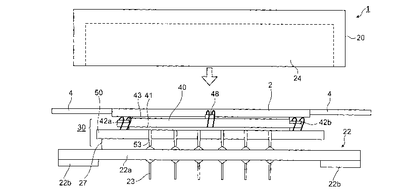
Fig. 1 is a perspective view showing the heater module
in accordance with this embodiment and an optical waveguide
module incorporating it therein, whereas Fig. 2 is a side
view of the optical waveguide module shown in Fig. 1. The
optical waveguide module 1 comprises an optical waveguide
device 2 made of quartz having a size of 50 mm x 10 mm x
1 mm, optical fibers 4 connected to both ends of the optical
wave guide device 2, a heater module 30 for heating the optical
waveguide device 2, and a case 20 for accommodating the optical
waveguide device 2 and heater module 30. The case 20 is
constituted by a package substrate 22, to which lead pins
23 for energizing the heater module 30 are soldered, for
supporting the heater module 30, and a cover 24 to be put
19
CA 02398971 2002-07-26
FP00-0256-00
on the package substrate 22. The package as a whole has a
size of 100 mm x 50 mm x 10 mm.
With reference to Figs. 3 to 5, the heater module 30
will now be explained in detail. The heater module 30
comprises a ceramics heater 40 having a size of 40 mm x 20
mm x 1 mm, and an insulating substrate 50 with a size of
60 mm x 30 mm x 2 mm for supporting the ceramics heater 40
and having a thermal insulating characteristic (see Fig.
5) . Fig. 3 is a plan view showing the inside of the ceramics
heater 40, whereas Fig. 4 is a sectional view of the ceramics
heater 40 taken along the line IV-IV in Fig. 3. As shown
in Figs. 3 and 4, the ceramics heater 40 is provided with
a heating circuit 42, adapted to generate heat when energized,
having a resistance value of about 0. 5 f~ to 10 ~2. Also, both
ends of the heating circuit 42 are provided with electrodes
42a, 42b for causing a current to flow through the heating
circuit 42, respectively.
A first AlN ceramics layer 44 is mounted as an over
layer (on the upper side in Fig. 4) for the heating circuit
42, whereas a second A1N ceramics layer 46 is mounted as
an underneath layer for the heating circuit 42.
Since the ceramics layer 44 is formed fromAlN (aluminum
nitride) having a high thermal conductivity in this
embodiment as such, the heat transmitted from the heating
circuit 42 diffuses substantially uniformly into the first
A1N ceramics layer 44, so that the optical waveguide device
CA 02398971 2002-07-26 - ---
FP00-0256-00
2 bonded to the upper face of the first A1N ceramics Layer
44 is uniformly heated, whereby the temperature uniformity
can be improved. Since A1N has a good moisture-resistant
characteristic, the heating circuit 42 does not change its
resistance value even when used continuously for a long term,
whereby a high reliability can be obtained. Further, since
the second A1N ceramics layer 46 is disposed beneath the
heating circuit 42, the ceramics heater 40 improves its
moisture-resistant characteristic, whereby the heating
circuit 42 can improve its durability. Specifically, since
the second A1N ceramics layer 46 keeps the heating circuit
42 from being exposed, the heating circuit 42 can be prevented
from short-circuiting and oxidizing.
Preferably, the total thickness of the first A1N
ceramics layer 44 and second ALN ceramics layer 46 is at
least 0.3 mm but not greater than 3.0 mm. When the total
thickness of A1N ceramics layers is less than 0.3 mm, the
heat generated by the . heater is hard to spread, whereby it
becomes difficult for the optical wave guide device 2 to have
a temperature uniformity of ~0.5°C or less. Also, when the
total thickness of A1N ceramics layers is less than 0.3 mm,
its mechanical strength is so low that handl ing such as bonding
of the optical waveguide device becomes quite difficult.
On the other hand, it will be unfavorable if the total thickness
of the first A1N ceramics layer 44 and second A1N ceramics
layer 46 exceeds 3.0 mm, since the optical waveguide module
21
CA 02398971 2002-07-26 - --
' ' FP00-0256-00
inevitably increases its thickness thereby, although the
temperature uniformity of optical waveguide device does not
deteriorate.
The heating circuit 42 can be formed from tungsten or
molybdenum which can be formed at the same time when the
A1N ceramics layers are molded and sintered, silver palladium
allowing a technique of forming and sintering the heating
circuit after A1N ceramics layers are once molded and sintered,
or the like as a main ingredient . Tungsten and molybdenum
can be formed simultaneously with A1N ceramics, thus being
advantageous in that cost can be lowered. On the other hand,
silver palladium is advantageous in that its resistance value
is easily controlled with a high precision. These materials
may be selected according to the order of precedence required
as the optical waveguide module. Here, heating materials
other than the foregoing materials do not deteriorate
advantages of the ceramics heater using A1N, so that they
can be used without any problem.
The thickness of the heating circuit 42 is not
restricted in particular. However, for example, it is
desirable that the thickness be controlled so as to become
at least 1 pm but not greater than 100 um when forming a
pattern by screen printing. If the thickness is less than
1 dun, the possibility of defects such as pattern losses
occurring will increase dramatically. On the other hand,
it will be unfavorable if the thickness exceeds 100 um, since
22
CA 02398971 2002-07-26 - --
' FP00-0256-00
defects of blotting and the like may occur frequently when
the heating circuit pattern is as narrow as about 0.2 mm.
For completely eliminating such defects, it is preferred
that the thickness be 50 um or less. Though a film thickness
of 1 um or less is possible when forming the heating circuit
42 from a thin film or the like, for example, it is necessary
that the film thickness be such a level that the film will
not break when a current flows therethrough.
As a protective layer for the heating circuit 42, a
glass coating film may be formed as well. For example, a
coating film mainly composed of silica glass may be formed
on the surface of heating circuit 42. Such a glass coating
film is further formed after the A1N ceramics layers and
heating circuit are once formed. Therefore, it is
advantageous in that the material of glass coating film can
be selected freely. Also, since the glass coating film has
a low thermal conductivity of 1 W/mK in general; it acts
as a kind of insulating layer when the optical waveguide
device 2 is mounted on the surface opposite from the glass
coating film, thereby improving the temperature uniformity
of optical waveguide device 2. Thus, forming the heating
circuit 42 with a coating film can improve the
moisture-resistant characteristic of ceramics heater 40.
Preferably, the thickness of glass coating film is at
least 1 um but not greater than 0.2 mm. More preferably,
it is at least 10 ~.un but not greater than 0.2 mm. When the
23
CA 02398971 2002-07-26
FP00-0256-00
film thickness is less than 1 um, it cannot cover the heating
circuit 42 uniformly, thus leaving anuncoatedpart. Further,
since differences in level exist between the heating circuit
42 and A1N ceramics 46, a film thickness of 10 um or greater
can fill the difference in level with a better yield. When
the film thickness exceeds 200 um, on the other hand, it
takes an enormous time to form the film not only from a thin
film but also by screen printing, which dramatically raises
the cost and thus is unfavorable. Nevertheless, there will
be no problem even if the coating film thickness is outside
the above-mentioned range as long as the heating circuit
42 can be protected thereby in a minimally required manner.
Also, since the ceramics heater 40 is supported by the
insulating substrate SO having a thermal insulating
characteristic as mentioned above in this embodiment, the
heat generated by the heating circuit 42 can be prevented
from being released from the insulating substrate 50 and
thereby making the temperature distribution uneven in the
ceramics heater 40, whereby the temperature uniformity of
the optical waveguide device 2 can further be improved. When
the insulating substrate 50 is not provided, in particular,
the ceramics heater 40 heats not only the optical waveguide
device 2 mounted thereon, but also members in contact with
the surface opposite from that mounted with the optical
waveguide device 2. Namely, when a member having a high
thermal conductivity or a member having a large heat capacity
24
CA 02398971 2002-07-26
r r
FP00-0256-00
is bonded to the surface of ceramics heater 40 opposite from
the optical waveguide device 2, the heat generated by the
ceramics heater 40 mainly flows into such a member rather
than the optical waveguide device 2, thereby deteriorating
the temperature uniformity of the optical waveguide device
2 and increasing the power consumption of ceramics heater.
Supporting the ceramics heater 40 with the insulating
substrate 50, by contrast, can prevent the heat generated
by the heating circuit 42 from being released from the
insulating substrate 50 and thereby making the temperature
distribution uneven in the ceramics heater 40.
Thermal simulations have proved it preferable for the
insulating substrate 50 to have a thermal conductivity of
50 W/mK or less in order to attain the effect mentioned above.
Also, since the heater module and optical waveguide module
can be simplified when wiring is provided within the
insulating substrate 50 so as to connect with the ceramics
heater electrically, it is preferred that the insulating
substrate 50 be made of a material which allows wiring to
be formed therewithin. For example, the insulating
substrate 50 may be made of a material containing alumina
and silica glass. Though the insulating substrate 50 is
formed from alumina and silica glass as main ingredients,
the thermalinsulating characteristic can further beimproved
if a resin and silica glass are employed as main ingredients .
In particular, it will be favorable if the insulating
CA 02398971 2002-07-26 - -'
FP00-0256-00
substrate 50 is formed from a resin, since the thermal
conductivity can be made 1 W/mK or less thereby. As a resin
material, glass epoxy resin, BT (bismaleimide-triazine)
resin, and the like, which are typically used in printed
circuit boards, can be used.
The ceramics heater 40 is prepared as follows. First,
the heating circuit 42 and electrodes 42a, 42b are printed
on a preform sheet of A1N ceramics with W paste . Subsequently,
a preform sheet of A1N ceramics is attached onto the heating
circuit 42, so as to yield a temporary form of heater. Then,
this temporary form is sintered in a nitrogen atmosphere
of 1700°C or higher, whereby the ceramics heater 40 is
completed.
Fig. 5 is a plan view showing the heater module 30.
As depicted, electrodes 52a to 52f are formed on the upper
face of the insulating substrate 50, whereas the electrodes
42a, 42b of ceramics heater 40 are connected to the electrodes
52a, 52f with conductors. Disposed on the upper face of the
ceramics heater 40 is a chip thermistor 48 for measuring
the temperature of heater, whereas the chip thermistor 48
is connected to the electrodes 52c, 52d with conductors.
Further, lead pins 53 are connected to the electrodes 52a
to 52f, respectively, and are bent at right angles as shown
in Fig. 2, so as to be soldered while being plugged into
insertingholes of the package substrate 22 . As a consequence,
the individual lead pins 53 are electrically connected to
26
CA 02398971 2002-07-26 -
' ' FP00-0256-00
their corresponding lead pins 23 of the package substrate
22. Also, since the electrodes 52a to 52f are formed on the
insulating substrate 50 as mentioned above, no long wires
are necessary for connecting the ceramics heater 40 to
external electrodes, which facilitates assembling and
packaging, thereby cutting down the cost.
Also, as shown in Fig. 2, the insulating substrate 50
and the ceramics heater 40 are bonded to each other with
a resin 41, whereas the ceramics heater 40 and the optical
waveguide device 2 are bonded to each other with a resin
43. While any of resins such as silicone resin and epoxy
resin used for bonding electronic parts can be used as the
bonding resin 41, silicone resin is used in this embodiment
in order to prevent deforming from occurring at the time
of bonding. Also, the first A1N ceramics layer 44 is disposed
as the uppermost layer of ceramics heater 40 as mentioned
above and thus can prevent the optical waveguide device 2
from warping, since A1N has a thermal expansion coefficient
close to that of glass or Si forming the optical waveguide
device 2 . The resin 43, which is used for bonding the optical
waveguide device and AlN in this embodiment, is silicone
resin. Each of the resins 41 and 43 has a thickness of about
10 um to 0.2 mm.
In general, the resin bonding strength of A1N has been
known to be lower than that of other oxide type ceramics
and the like. The resin bonding strength is caused by the
27
CA 02398971 2002-07-26
T
FP00-0256-00
hydrogen bond formed between the -OH group of resin and the
-O group of a metal surface, the anchor effect between
materials, and their interaction. Since the surface of A1N
is a nitride, only the anchor effect can contribute to bonding .
As a consequence, there is a possibility of its bonding
strength to a resin deteriorating depending on the surface
state of A1N ceramics and the like. Therefore, it is
preferred that the reliability in resin bonding strength
of A1N be enhanced. For enhancing the bonding strength
between the AlN ceramics layer and resin, two kinds of methods,
i.e., a first method of enhancing the anchor effect and a
second method of providing a layer adapted to raise the resin
strength, can be considered.
As a result of various studies concerning conditions
necessary for attaining a sufficient anchor effect, it has
been found that the first method can be achieved i f the surface
roughness of the surface of A1N to be bonded to the resin
is controlled strictly. Namely, it has been concluded that,
when bonding the A1N heater to a package having an optical
waveguide device, an insulating substrate, and the like,
a sufficient bonding strength can be achieved if the ceramics
heater 40 to be bonded to the resin is controlled so as to
have a surface roughness of at least 0.05 ~.un but not greater
than 10 Vim, preferably at least 0.1 um but not greater than
10 um, in terms of Ra. When the A1N surface roughness is
less than 0.05 um, a sufficient anchor effect cannot be
28
CA 02398971 2002-07-26 - w-
' FP00-0256-00
attained between A1N and the resin, whereby defects of the
resin bonding face peeling, dropping, and so forth may occur
during reliability tests or uses of the optical waveguide
module. Though sufficient bonding can be realized if the
above-mentioned A1N surface roughness is at least 0.05 um
when a resin having a high bonding strength such as silicone
resin is used, it is preferred that the A1N surface roughness
be at least 0.1 ~.un in order to realize sufficient bonding
in all of various other resins. If the A1N surface roughness
exceeds 10 um, on the other hand, bubbles and the like will
be easier to flow into the gap between A1N and the resin,
whereby a sufficient anchor effect may not be obtained.
Further, the resin and bubbles exist randomly in the resin
bondinglayer, thereby greatly deteriorating the temperature
uniformity. Though the entanglement of bubbles can be
prevented from occurring if the A1N surface roughness is
100 um or less when a resin with a relatively high fluidity
yielding a viscosity of about 10000 cps at the time of
application is employed, it is preferred that the A1N surface
roughness be 10 um or less in order to prevent bubbles from
being entangled even when viscosity rises due to changes
in other resins with time.
As a result of various studies concerning a condition
necessary for obtaining a layer adapted to enhance the resin
strength as the second technique for enhancing the bonding
strength between the A1N ceramics layer and the resin, it
29
CA 02398971 2002-07-26 - ---
FP00-0256-00
has been found the most effective to coat the resin bonding
surface of the ceramics heater 40 with an A1 layer by vapor
deposition or a layer mainly composed of silica glass.
The layer adapted to enhance the resin strength
necessitates a layer containing OH group or -OH group so
as to strengthen the hydrogen bond with the resin, or a layer
adapted to enhance the anchor strength. As the layer for
strengthening the hydrogen bond to the resin, an oxide or
a metal can be considered.
As such an oxide, alumina can be considered, for example .
However, oxides of ceramics such as alumina are problematic
in that the cost of heater becomes drastically higher, since
the temperature necessary for forming a layer rises. By
contrast, silica glass can suppress the cost to a low level,
since its layer forming temperature can be made lower than
that of alumina. Also, since silica glass can be used as
a protective film for the heating circuit 42 of ceramics
heater 40 as well, the resin bonding strength and reliability
of the ceramics heater 40 can be improved at the same time
in a single step when forming a silica glass layer, whereby
the A1N ceramics heater having excellent characteristics
can be made at a low cost.
As with the above-mentioned glass coating film of
heating circuit, the silica glass layer formed on the surface
of ceramics heater 40 preferably has a thickness of at least
1 um but not greater than 0.5 mm, more preferably at least
CA 02398971 2002-07-26 ' '-
. ~ FP00-0256-00
dun but not greater than 0.1 mm. When the thickness of
silica glass layer is less than 1 um, it cannot cover A1N
ceramics uniformly, thus leaving an uncoated part, whereby
the resin strength cannot be enhanced sufficiently. When
5 forming a protective layer for the heater in the same process,
differences in level exist in the heater layer, whereby the
layer thickness is required to be at least 10 um in order
to fill the differences in level. When the silica glass layer
has a thickness exceeding 500 uzn, on the other hand, glass
10 itself may break and cannot be used after a reliability test
since the strength of glass itself is low, although the resin
bonding is sufficient. Though a film thickness smaller than
that can be used, an enormous time is necessary for forming
a film thicker than 100 dun, which dramatically increases
the cost, whereby it is further preferred that the layer
thickness be 100 um or less.
Though the forming of silica glass layer is not
restricted in particular, a method comprising the steps of
printing glass paste by use of screen printing or the like
and baking it upon firing, and the like may be used since
the silica glass layer is required to be formed in limited
areas such as the resin bonding part and heater part.
In the forming of a layer using a metal, on the other
hand, metals other than Al, Ni, Au, and the like oxidize,
thus corroding the surface thereof and failing to keep a
bonding strength at the same. On the other hand, Ni and Au
31
CA 02398971 2002-07-26 - --
y .
' ' FP00-0256-00
used as a protective film for metals have a smaller quantity
of OH group and -0 group on the surface, thus yielding a
very low bonding strength with respect to the resin after
a reliability test in particular. By contrast, Al is
favorable in that its resin strength is relatively high since
its surface is always oxidized. It has further been found
that the resin strength does not increase but decreases even
when the A1 film is intentionally oxidized more than a
naturally oxidizedfilm. Furtherstudies have revealed that
the resin bonding strength varies greatly depending on the
method of forming an Al film. Namely, when the A1 film formed
by vapor deposition is used in a naturally oxidized state,
an A1N ceramics heater having a very high resin bonding
strength can be prepared.
Investigations of reasons why the A1 film formed by
vapor deposition has a high resin strength have revealed
that a microscopic anchor effect contributes thereto. When
an Al film is formed by vapor deposition or the like, polygonal
crystalparticlesare generated. Though a minute difference
of 1 um or less in level exists between the crystal particles,
this difference in level cannot be detected at the time when
measuring thesurface roughness. Thiscrystalparticlesize
and its accompanying difference between crystals in level
generate a sufficient anchor effect. Namely, when the
crystal particle size is controlled so as to become at least
0.1 um but not greater than 10 um, a sufficient anchor effect
32
CA 02398971 2002-07-26 - --
' FP00-0256-00
can be yielded. When the crystal particle size is less than
0. 1 um, the resin used for bonding cannot sufficiently enter
gaps between crystals, whereby holes are likely to occur.
The breakage of Bond is likely to occur from the holes acting
as starting points. When the crystal 'particle size exceeds
um, though the resin can enter gaps between crystals,
the number of particles per area contributing to the anchor
effect becomessmaller,whereby asufficient bondingstrength
cannot be obtained.
10 In a structure which can yield a sufficient anchor
effect as mentioned above, it is not required to form an
oxidized film in particular. Namely, a naturally oxidized
film thickness of at least 10 x 10-1° m but not greater than
800 x 10-1° m is desirable . In the state without a naturally
oxidized film, no hydrogen bond occurs with respect to the
resin, whereby a sufficient bonding strength cannot be
maintained. When an oxidized film having a thickness
exceeding 800 X 10-1° m is formed, the bonding strength between
the oxidized film and a matrix metal cannot be secured since
the metal oxide film is brittle, though the bonding strength
between the resin and oxidized film is unproblematic.
The A1 film thickness to be formed is desirably at least
1 um but not greater than 100 um. When the A1 film thickness
is less than 1 um, a structure is not sufficient for yielding
an anchor effect. That exceeding 100 ~,im is unfavorable since
breakage is likely to occur within the film. Also, that
33
CA 02398971 2002-07-26 - --
' FP00-0256-00
exceeding 20 um is problematic in terms of economy since
the cost and time for forming the film become enormous.
Therefore, the A1 film thickness is more preferably at least
1 dam but not greater than 20 Vim.
The A1 film to be formed may be either A1 or an Al alloy.
Desirably, the A1 alloy has a purity of 99.9 wt$ or higher,
since its composition is hard to control at the time of forming
the film, and since its adhesion to the matrix is likely
to fluctuate. Further, an A1 film of 99.9 wt~ or higher is
preferable since no fluctuation in adhesion to the matrix
occurs therein. Since vapor deposition can apply an Al films
to various materials in a relatively simple manner, it is
preferred that vapor deposition of A1 film be applied to
other members to be bonded to a resin in the optical waveguide
module whenever possible, whereby the resin bonding strength
can greatly beimproved. Whether vapor depositionisapplied
or not may be determined in view of whether an insulating
characteristic is necessary or not; since A1 is a metal,
and the increase in cost caused by vapor deposition.
The case 20 of optical waveguide module 1 will now be
explained with reference to Figs . 1 and 2 . Two opposed faces
of the cover 24 of case 20 are formed with insertion ports
24a, 24b (see Fig. 1) for inserting the optical fibers 4
therethrough. The package substrate 22 has a flat plate 22a
to which the lead pins 23 are soldered, and support plates
22b, 22b bonded to both lower ends of the flat plate 22a,
34
CA 02398971 2002-07-26
FP00-0256-00
respectively. Providing the support plates 22b as such can
prevent an excessive load from being applied to the lead
pins 23 when implementing the optical waveguide module 1
into a system board or the like. The cover 24 and the package
substrate 22 are bonded to each other with a resin.
The cover 24 of case 20 and the package substrate 22
are formed from copper tungsten as a main ingredient. As
a consequence, the temperature uniformity in the case 20
is high, whereby the temperature uniformity of optical
waveguide device 2 can be improved. Similar effects can also
be obtained when the case 20 is formed from cobalt, iron,
nickel, alumina, or aluminum nitride as a main ingredient.
Results of thermal simulations have revealed that the case
preferably has a thermal conductivity of 10 W/mK or higher
15 in order to improve the temperature uniformity of the optical
waveguide device 2.
When the case 20 is formed from a resin or silica glass
as a main ingredient, the heat within the case 20 can be
restrained from being released to the outside, since these
20 materials have a high thermal insulating characteristic.
As the resin forming the case 20, ABS resin, polyoxymethylene
resin, polyether ether ketone resin, styrene resin, acrylic
resin, epoxy resin, phenol resin, urea resin, melanin resin,
silicone resin, fluorine resin, polycarbonate resin,
polyphenylene sulfide resin, and the like, for example, can
be used. Results of thermal simulations have revealed that
CA 02398971 2002-07-26 - '
FP00-0256-00
the thermal conductivity of such resins is preferably 1 W/mK
or less in order to improve the temperature uniformity of
optical waveguide device 2. Further, glass fiber and the
like may be mixed into these resins in order to improve the
strength thereof . In this case, since these materials have
a high thermal insulating characteristic, the heat within
the case can be prevented from being released to the outside,
whereby the optical wave guide device 2 can be prevented from
lowering its temperature. Also, the case materials for
improving the temperature uniformity and thoseforimproving
the thermal insulating characteristic may be formed into
multiple layers or used in combination.
Also, as shown in Fig. 2, an insulating layer 27 having
a thermal conductivity of 0.5 W/mK or less is disposed about
the heater module 30 (between the package substrate 22 and
the insulating substrate 50). In this embodiment, the
insulating layer 27 is an air layer having a thickness of
1 mm. When the insulating layer 27 is provided as such, heat
can efficiently be transmitted to the optical waveguide
device 2. Further, the inner face of the cover 24 of case
20 is provided with an insulating layer formed by an air
layer in order to restrain the heat of the optical waveguide
device 2 from being released to the outside of the case 20.
Preferably, the insulating layer 27 as an air layer
has a thickness within the range of at least 0.01 mm but
not greater than 5 mm, For yielding a high temperature
36
CA 02398971 2002-07-26 - -
' FP00-0256-00
uniformity, it is important that no heat convection occur
in the air layer. As a result of studies concerning
conditions therefor by means of thermohydrodynamic
simulations and experiments, it has been concluded that heat
convection can greatly be suppressed if the air layer
thickness is 5 mm or less, whereby a high temperature
uniformity of the ceramics heater 40 can be secured. Though
convection is less likely to occur as the air layer is thinner,
the insulating substrate 50 and the package substrate 22
may come into contact with each other due to distortions
in the heater module and optical waveguide module caused
by heating of the heater, so that the air layerpartlydecreases,
whereby a high temperature uniformity cannot be attained
if the thickness is less than 0,01 mm.
The thickness (thickness reduction) of the heater
module 30 and optical waveguide module 1 will now be explained
in detail.
If the difference in CTE between the ceramics heater
40 and optical waveguide device 2 is 3 x 10⁻⁶ to 5 x 10⁻⁶/°C
or greater when bonding them to each other, there is a fear
of an excessive thermal stress acting on the optical waveguide
device, thereby disturbing wavelength selectivity and
switching characteristics. Conventionally used alumina
heaters have a CTE of 7 x 10⁻⁶/ °C while exhibiting a low thermal
conductivity of 20 W/mK, whereby a heat spreader has been
indispensable. Since such a heat spreader has a thickness
37
CA 02398971 2002-07-26 - --
FP00-0256-00
of about 3 mm in general, it has been impossible for the
optical waveguide module to reduce its thickness. Though
a method in which the gap between the heat spreader and optical
waveguide device is filled with an oil compound or grease,
which is a fluid even after bonding, and then only several
points at end parts are fixed with a resin, and the like
have been taken into consideration in order to reduce the
stress on the optical waveguide device, even the thermal
stress occurring upon fixing with the resin at several points
may become problematic to the optical waveguide device, so
that they have not been universally usable techniques, and
it has been impossible to eliminate the heat spreader, whereby
the optical waveguide module has been unable to reduce its
thickness.
By contrast, A1N of the ceramics heater 40 in this
embodiment has a thermal conductivity of 170 W/mK, so that
there is no need to use a heat spreader, whereby the thickness
of optical waveguide module can be reduced greatly.
Further, while the resin 43 bonds the optical waveguide
device 2 and the ceramics heater 40 to each other, this resin
43 is an adhesive attaining a solid form after bonding.
Therefore, no fluctuations occur in the resin thickness,
so that the resin does not flow during operations of the
optical waveguide module. Desirably, the resin used for
bonding the optical waveguide device 2 and the ceramics heater
40 to each other is a resin having a high thermal conductivity
38
CA 02398971 2002-07-26 - "'
FP00-0256-00
of about 0.5 W/mK or more containing a filler such as a metal
or ceramics. Though the optical waveguide device 2 is
uniformly heated by the ceramics heater 40, there is a fear
of the optical waveguide device 2 deteriorating its
temperature uniformity when a resin having a thermal
conductivity lower than 0.5 W/mK is used.
Also, it is possible to use a method in which the gap
between the optical waveguide device 2 and ceramics heater
40 is filled with the above-mentioned oil compound or grease,
which is a fluid even after bonding, in phace of the resin
43 and then only several points at end parts are fixed with
a resin, since the difference in CTE between the optical
waveguide device 2 and ceramics heater 40 is so small that
no stress is applied to the optical waveguide device 2.
However, the thickness of oil compound and grease must be
managed strictly when this method is employed.
Preferably, the resin 43 has a thickness of at least
10 pnn but not greater than 500 dun. Since the bonding resin
has a Young' s modulus smaller than that of other constituent
materials by at least one digit, it acts to absorb the thermal
stress occurring upon bonding. However, it will be
unfavorable if the resin 43 has a thickness smaller than
10 dun, since absorbing stress cannot fully be exhibited
thereby, so that the stress on the optical waveguide device
2 becomes greater. Since the resin 43 has a thermal
conductivity lower than that of A1N and the like, its
39
CA 02398971 2002-07-26
FP00-0256-00
temperature uniformity deterioratesasthethicknessthereof
increases. It will be unfavorable if the resin 43 has a
thickness exceeding 10 um, since the temperature uniformity
deteriorates.
Further, as for the power consumption of the ceramics
heater 40 and optical waveguide module l, the power
consumption can be reduced greatly in this embodiment as
compared with conventionalcasesusing alumina heaters,since
it is unnecessary to heat a heat spreader made of a Cu alloy
or the like indispensable when using an alumina heater.
Also, the following safe design can be provided in the
optical waveguide module 1 in accordance with this embodiment .
Namely, a part of the heating circuit 42 may be formed by
an alloy of tin and lead, or the heating circuit 42 and a
terminal connected to an external power supply may be
connected to each other with a wire formed from an alloy
of tin and lead, so that thus formed part breaks when the
temperature of heating circuit 42 is at the melting point
of the alloy or higher, whereby no current flows through
the heating circuit. Such a design can prevent the heater
module from breaking, igniting, and so forth when temperature
rises due to malfunctions of the heater module.
For example, when an alloy composed of 40 wt~ of tin
and 60 wt$ of lead is used, it will break at a temperature
not higher than about 200°C, whereby the bonding resin and
resins of the case and the like will not be damaged. In place
CA 02398971 2002-07-26 - "'
FP00-0256-00
of the alloy of tin and lead, other low-melting alloys may
also be used.
When characteristics of the optical waveguide module
1 as explained in the foregoing were investigated, the
following results were obtained. As for the temperature
uniformity, viewing with a thermoviewer at an ambient
temperature of 0°C with the ceramics heater 40 having a
temperature of 80°C revealed that the temperature
distribution within the optical waveguide device 2 was
suppressed to ~0 . 4 °C or less . Also, in order to measure the
temperature controllability, the following experiment was
carried out . Namely, the optical waveguide was put into a
thermostat, the temperature of which was changed so as to
be held at -40°C for an hour, raised to 70°C in an hour,
held at 70°C for an hour, and lowered to -40°C in an hour.
The temperature on the optical waveguide device at that time
was measured, whereby the difference between the maximum
temperature and minimum temperature was taken as an index
for determining the temperature controllability. As a
result, it was found that the optical waveguide device in
thisembodiment exhibited a temperaturefluctuation of ~0.7°C
or less and thus being less susceptible to influences of
external temperature. Also, the warping of the ceramics
heater 40 and optical waveguide device 2 was smaller, no
anisotropy was seen in optical waveguide characteristics,
and no defects such as increases in loss and dependence on
41
CA 02398971 2002-07-26 - --
FP00-0256-00
polarization caused by switching characteristics and
birefringence did not occur. Further, since the insulating
characteristic within the case improved, this embodiment
was capable of suppressing the power consumption to 4 W or
less as compared with conventional cases necessitating a
power consumption of 5 W when using a Peltier device.
Second Embodiment
A second embodiment of the optical waveguide module
in accordance with the present invention will now be explained
with reference to Figs. 6 to 8. This embodiment differs from
the first embodiment mainly in the structure of insulating
substrate 50. In the following, points different from the
first embodiment will mainly be explained.
As shown in Fig. 6, the insulating substrate 50 is formed
with three protrusions 62 for supporting the ceramics heater
40. The upper face of each protrusion 62 is coated with a
resin, thereby attaining adhesion to the ceramics heater
40. Since the ce-ramics heater 40 is in contact with the
insulating substrate SO not totally but partly in this
embodiment as such, warping is harder to occur in the ceramics
heater 40, and the resin for bonding the insulating substrate
50 and the ceramics heater 40 to each other can be prevented
from peeling off from the ceramics heater 40. Here, instead
of coating all the protrusions 62 with the resin for adhesion
as in this embodiment, the resin may be applied to one
protrusion 62 alone. For example, when only the center
42
CA 02398971 2002-07-26 - --
' FP00-0256-00
protrusion 62 is coated with a resin, both end parts of the
ceramics heater 40 can expand/contract freely, whereby the
warping of ceramics heater 40 can further be reduced.
In this embodiment, an air layer 64 is formed about
each protrusion 62, i . a . , between the bottom face of ceramics
heater 40 and the surface of insulating substrate 50 facing
the same. Therefore, the air layer 64 acts as an insulating
layer, whereby the heat from the ceramics heater 40 can be
restrainedfrom being released from theinsulatingsubstrate
50 side . In this embodiment, the air layer has a thickness
of 0.2 mm.
Preferably, the air layer has a thickness of at least
0.01 mm but not greater than 5 mm. For attaining a high
temperature uniformity, it is important that no heat
convection occur in the air layer. As a result of studies
concerning conditions therefor by means of
thermohydrodynamic simulations and experiments, it has been
concluded that heat convection can greatly be suppressed
if the air layer thickness is 5 mm or less, whereby a high
temperature uniformity of the ceramics heater 40 can be
secured. Though heat convection is less likely to occur as
the air layer is thinner, the ceramics heater and its
supporting insulating substrate or the like may come into
contact with each other due to distortions in the heater
module and optical waveguide module caused by heating of
the heater if the thickness is less than 0.01 mm, thereby
43
CA 02398971 2002-07-26 - --
' ' FP00-0256-00
partly decreasing the air layer, thus failing to achieve
a high temperature uniformity.
Also, as shown in Fig. 7, pressing parts (pressing
means? 70 for pressing the ceramics heater 40 toward the
insulating substrate 50 are provided in this embodiment.
Each pressing part 70 is constituted by a pressure plate
72 mounted on the upper face of ceramics heater 40, and a
screw 74 for fastening the pressure plate 72 to the insulating
substrate 50. When the screw 74 is fastened firmly, the
ceramics heater 40 is pressed against the insulating
substrate 50. Since such pressing parts 70 pressed the
ceramics heater 40 toward the insulating substrate, favorable
results were obtained in vibration fatigue tests, constant
acceleration tests, and moisture-resistant characteristic
tests. Here, as depicted, the insulating substrate 50 is
formed with a plurality of through holes 55, which are
electrically connected to the heating circuit 42 of ceramics
heater 40 with conductors. Also, as shown in Fig. 6,-the
lead pins 23 passing through the package substrate are
inserted through the through holes 55.
Fig. 8 is a sectional view of the ceramics heater 40
in accordance with this embodiment. As depicted, the
ceramics heater 40 in accordance with this embodiment
comprises the heating circuit 42 made of silver palladium,
an AlN ceramics layer 44 stacked thereon, and a coating film
45 mainly composed of silica glass disposed beneath the
44
CA 02398971 2002-07-26 - --
' ' FP00-0256-00
heating circuit 42. Forming the coating film 45 on the
surface of ceramics heater 40 as such can improve the
moisture-resistant characteristic of ceramics heater 40.
Also, when bonding the ceramics heater 40 and the insulating
substrate 50 to each other with a resin, the adhesion of
resin to the ceramics heater 40 can be improved.
Third Embodiment
A third embodiment of the optical waveguide module in
accordance with the present invention will now be explained
with reference to Fig. 9. This embodiment differs from the
first embodiment in the structure of case 20. As depicted,
the inside of the cover 24 of case 20 is provided with four
partition walls 29 extending from a surface 24r facing the
optical waveguide device 2 toward the optical waveguide
device 2 . The height of partition walls 29 is such that lower
ends of the partition walls 29 are not in contact with the
optical waveguide device 2 in a state where the cover 24
is put on the package substrate 22 . Providing such partition
walls 29 can reduce the convection within the case 20, i . a . ,
the convection on the optical waveguide device 2, whereby
the temperature uniformity of optical waveguide device 2
can be improved.
Fourth Embodiment
A fourth embodiment of the optical waveguide module
in accordance with the present invention will now be explained
with reference to Fig. 10. This embodiment differs from the
CA 02398971 2002-07-26 -
' " FP00-0256-00
first embodiment in the method of attaching the chip
thermistor 48 and structures of the case 20 and cover 24.
First, the method of attaching the chip thermistor 48
will be explained in detail. As shown in Fig. 10, the
thermistor (temperature detecting device) 48 for detecting
the temperature of ceramics heater 40 is mounted to the bottom
face of ceramics heater 40, i . a . , the surface thereof opposite
from the surface mounted with the optical waveguide device
2. As a consequence, there is no need for securing an area
for mounting the thermistor 48 in the upper face of ceramics
heater 40. Therefore, the area of ceramics heater 40 can
be made smaller than that in the first embodiment, whereby
the heater module 30 can reduce its size. Also, the heating
circuit 42 can be made smaller, so as to lower the power
consumption. While the first embodiment has a ceramics
heater size of 40 mm x 20 mm x 1 mm, a heater module size
of 60 mm x 30 mm x 1 mm, and a heater power consumption of
4 W at an ambient temperature of 0°C and a heater control
temperature of 80°C, this embodiment can reduce the heater
size to 40 mm x 12 mm x 1 mm, the heater module size to 60
mm x 20 mm x 1 mm, and the power consumption to 3.5 W. The
insulating substrate 50 is formed with a cutout, in which
an electrode pad 78 connecting with the thermistor 48 is
disposed.
In the conventionally used alumina heater, since
alumina has a low thermal conductivity, there is a large
46
CA 02398971 2002-07-26 - --
' ' FP00-0256-00
temperaturedifference betweenthesurface ofheater mounting
the optical waveguide device and the surface opposite
therefrom, whereby it has been incapable of accurately
measuring the temperature of optical waveguide device at
the oppositesurface. By contrast, thermalsimulationshave
found it possible to estimate the temperature of optical
waveguide device 2 accurately at the surface opposite from
the surface for mounting the optical waveguide device when
an A1N heater is used.
Fig. 11 is an enlarged perspective view showing the
vicinity of the cutout 76. As shown in Figs. 10 and 11, the
insulating substrate 50 has an upper layer 52 and a lower
layer 54, whereas the bottom face of upper layer 52 is formed
with the electrode pad 78 . More speci fically, the upper layer
52 is formed with a through hole 52h, whereas the lower layer
54 is formed with a through hole 54h such that a part of
the bottom face of upper layer 52 is exposed. Also, they
are configured such that at least a part of the electrode
pad 78 is positioned at the exposing part of the bottom face
of upper layer 52.
The bottom face of ceramics heater 40 is formed with
an electrode pad 80, the thermistor 48 and the electrode
pad 80 are connected to each other with a wire 73, and the
electrode pads 78 and 80 are connected to each other with
a wire 75 . Since the wire 75 can be connected to the electrode
pad 78 by way of the cutout 7 6, i . a . , through holes 52h and
47
CA 02398971 2002-07-26 - --
' ' FP00-0256-00
54h, this embodiment can simplify wiring as compared with
cases where the wire 75 travels about the insulating substrate
50 and the like.
Also, since the wire connecting the thermistor 48 to
an external electrode for supplying electric power thereto
comes into contact with the ceramics heater 40 at the electrode
pad 80, thereby attaining a temperature substantially equal
to that of the ceramics heater 40, the temperature measurement
for the ceramics heater 40 is less likely to be affected
by the ambient temperature, whereby appropriate temperature
measurement can be carried out.
The electrode pad 78 is connected to a lead pin 23 shown
in Fig. 10, whereby continuity is established between the
thermistor 48 and an external device. Such a thermistor
electrode structure can prevent the thermistor electrode
from lowering its temperature. When measuring the
temperature controllability in the case where the ambient
temperature was -40°C to 70°C, the temperature of ceramics
heater 70 was found to be ~0.5°C or less, thus being less
susceptible to the external temperature as compared with
~0.7°C in the first embodiment not subjected to the foregoing
processing.
The case 20 of optical waveguide module 1 will now be
explained with reference to Fig. 10. Two opposite faces of
the cover 24 of case 20 are formed with insertion ports 24a,
24b for inserting optical fibers 4 therethrough. Two sheets
48
CA 02398971 2002-07-26 -
' FP00-0256-00
82, 84 are disposed in the cover 24 so as to be separated
from its inner wall face by a predetermined distance . Each
of the sheets 82, 84 is secured to a protrusion 24c with
an adhesive. Specifically, the upper sheet 82 is secured
to the center protrusion 24c, whereas the lower sheet 84
is connected to protrusions 24c at both ends . On the other
hand, the package substrate 22 is provided with two sheets
86, 88 separated from its upper face by a predetermined
distance. The outer peripheral part of each of the sheets
86, 88 is supported by a supporting member 89.
When the sheets 82, 84, 86, 88 are attached to the case
with a predetermined distance .from the inner wall face
thereof as such, the convection can be reduced between the
inner wall face of case 20 and each sheet 82, 84, 86, 88,
15 whereas an air layer is formed and acts as an insulating
layer. This makes the heat of ceramics heater 40 harder to
be released to the outside, whereby the optical waveguide
device 2, which is an object to be heated, becomes easier
to heat. The number of sheets is not limited to 2, but may
20 be 1 or 3 or more.
Though the optical waveguide device 2 made of quartz
is used in the first to fourth embodiments, a device using
silica prepared on an Si substrate, and a device made of
LiNb03 may also be used instead. Effects similar to those
of each embodiment can be obtained in this case as well.
Fifth Embodiment
49
CA 02398971 2002-07-26 - --
FP00-0256-00
A fifth embodiment of the optical waveguide module in
accordance with the present invention will now be explained
with reference to Fig. 12. This embodiment differs from the
first embodiment in the structure in which a matching plate
92 for matching CTE is inserted between the optical waveguide
device 2 and the ceramics heater 40. As the matching plate
92, one having difference of 3 x 10⁻⁶/°C or less from the
optical waveguide device 2 at room temperature in CTE is
used.
Since the optical waveguide device 2 made of quartz
(having a CTE of 0.5 x 10⁻⁶/°C) is used, an Fe-Ni alloy having
a CTE of 2 . 0 x 10-6/ °C is employed as the matching plate 92
in this embodiment. The matching plate 92 has a size of 40
mm X 20 mm x 0.5 mm.
Providing such a matching plate 92 can reduce the stress
on the optical waveguide device 2 . Hence, for measuring the
stress on the optical waveguide device 2, a strain gauge
was attached to the upper center part (the face opposite
from the face joined to the inserted plate) , and the difference
in stress acting on the optical waveguide device 2 between
the first embodiment and this embodiment was measured. As
a result, it has been found that the thermal stress acting
on the optical waveguide device 2 in this embodiment can
be reduced to 1 / 3 that o f the firs t embodiment . Though the
first embodiment can sufficiently be used as an optical
waveguide module, the effect lowering thermal stress in this
CA 02398971 2002-07-26 -
V
' FP00-0256-00
embodiment is considered be quite advantageous in view of
severer requirements which will be demanded in optical
waveguide modules from now on.
When similar experiments were carried out with the
optical waveguide device 2 changed to a device using silica
(having a CTE of 1.3 x 10⁻⁶/°C) prepared on an Si substrate,
results substantially the same as those in the case of quartz
were obtained.
Also, substantially the same favorable results were
obtained in this embodiment when similar experiments were
carried out with the optical waveguide device 2 and inserted
plate 2 changed to LiNb03 (having a CTE of 15 x 10-6/°C) and
a Cu alloy (having a CTE of 16 x 10-6/°C), respectively.
Sixth Embodiment
A sixth embodiment of the optical waveguide module in
accordance with the present invention will now be explained
with reference to the perspective view shown in Fig. 13 and
the side view shown in Fig. 14. The optical waveguide device
made of quartz in this embodiment has a larger size, i.e.,
30mm (L) x30mm (W) x lmm (H) , than that of the first embodiment.
As a consequence, dimensions of the optical waveguide module
are made different. The ceramics heater 40 has a size of
40 mm x 25 mm x 1 mm, the heater module 30 has a size of
50 mm x 40 mm x 2 mm, and the whole package has a size of
100 mm x 60 mm x 10 mm.
As the size of optical wave guide device 2 is made greater,
51
CA 02398971 2002-07-26 -
.
' ' FP00-0256-00
it becomes harder to secure a space formounting the thermistor
48 in the upper part of ceramics heater 40, i . a . , the surface
joined to the optical waveguide device 2, whereby the
thermistor 48 is mounted to the lower part of ceramics heater
40, i.e., on the surface opposite from the surface joined
to the optical waveguide device 2.' The optical waveguide
device 2 and the optical fiber 4 are connected each other
with a fiber array 96. While the insulating substrate 50
and package substrate 22 are formed with an air layer 27
as an insulating layer, the insulating substrate 50 is secured
onto the package substrate 22 by way of a spacer 94 so as
to be stabilized structurally even when the air layer 27
is formed.
Investigations of characteristics of the foregoing
optical waveguide module 1 yielded the following results.
As for temperature uniformity, viewing with a thermoviewer
at an ambient temperature of 0°C with the ceramics heater
40 having a temperature at 80°C revealed that the temperature
distribution within the optical waveguide device 2 was
suppressed to ~0.4°C or less. As for temperature
controllability, it was found that, even when the ambient
temperature was changed within the range from -40°C to 70°C,
the ceramics heater 40 merely exhibited a temperature change
of ~0. 5°C or less, thus being harder to be affected by external
temperature. Also, warping was small in the ceramics heater
40 and optical waveguide device 2, no anisotropy was observed
52
CA 02398971 2002-07-26 - --
FP00-0256-00
in optical waveguide characteristics, and no defects of
increases in loss, dependence on polarization caused by
switching characteristics and birefringence, and the like
occurred. Further, since the thermal insulating
characteristic withinthe case wasimproved, thisembodiment
was capable of suppressing the power consumption to 4 W or
less as well.
In this embodiment, the cover 24 is integral, so as
to join the insulating substrate 22. In this form, however,
there are cases where the optical fiber 4 is hard to attach.
In these cases, the form may be changed such that the cover
24 is split into a side wall part 24x formed like a square
tube and a top part 24y, the optical waveguide device 2 and
optical fiber 4 are mounted in a state where the package
substrate 22 and the side wall part 24x are once bonded to
each other, and then the top part 24y is bonded or screwed
thereto.
Seventh embodiment
A seventh embodiment of the optical waveguide module
in accordance with the present invention will now be explained
with reference to the perspective view shown in Fig. 15 and
the side view shown in Fig. 16. This embodiment differs from
the sixth embodiment in dimensions of the ceramics heater
40. Detailed investigations of characteristics of the
optical waveguide device 2 have revealed that an area
requiring temperature uniformity does not cover the whole
53
CA 02398971 2002-07-26 - -
FP00-0256-00
optical waveguide device 2, but is limited to the ceramics
heater and its surroundings . Specifically, it has been found
to be limited to an area of about 10 mm x 10 mm about the
ceramicsheater. Therefore, in thisembodiment, thesurface
40a of ceramics heater 40 for mounting the optical waveguide
device 2 has an area smaller than that of the surface of
optical waveguide device 2 facing the surface 40a. When the
heating surface of ceramics heater 40 is made smaller than
the optical waveguide device 2 as such, the power consumption
can further be lowered. Specifically, by a design utilizing
thermal simulations, the ceramics heater 40 is made with
a size of 15 mm x 15 mm x 1 mm.
Investigations of characteristics of the foregoing
optical waveguide module 1 yielded the following results.
As for temperature uniformity, uiewing with a thermoviewer
at an ambient temperature of 0°C with the ceramics heater
40 having a temperature of 80°C revealed that the temperature
distribution within the area of 10 mm X 10 mm necessitating
temperature uniformity inside the optical waveguide device
2 was suppressed to ~0.4°C or less. As for temperature
controllability, it was found that, even when the ambient
temperature was changed within the range from -40°C to 70°C,
the ceramics heater 40 merely exhibited a temperature change
of ~0 . 5°C or less, thus being harder to be affected by external
temperature. Since the size of ceramics heater 40 was made
smaller, it was possible for this embodiment to suppress
54
CA 02398971 2002-07-26 - '-
FP00-0256-00
the power consumption to 2 W or less, as compared with the
sixth embodiment yielding a power consumption of 4 W.
Eighth Embodiment
An eighth embodiment of the optical waveguide module
in accordance with the present invention will now be explained
with reference to the perspective view shown in Fig. 17 and
the side view shown in Fig. 18 . This embodiment differs from
the eighth embodiment in the matching plate 92 (whose cross
section is shown in Fig. 18) disposed so as to surround the
ceramics heater 40. As the matching plate 92, one having
difference of 3 x 10⁻⁶/°C or less from the optical wave guide
device 2 at room temperature in CTE is used.
Since the optical waveguide device 2 made of quartz
(having a CTE of 0.5 x 10⁻⁶/°C) is used, an Fe-Ni alloy having
a CTE of 2.0 x 10⁻⁶/°C is employed as the matching plate 92
in this embodiment. The matching plate 92 has a size of 40
mm X 25 mm X 1 mm, which is identical to the size of ceramics
heater 40 used in the sixth embodiment. Also, a hollow part
of 15.5 mm x 15.5 mm is formed at the center by boring, so
that the ceramics heater 40 having a size of 15 mm x 15 mm
1 mm can fit therein.
Since the matching plate 92 surrounding the ceramics
heater 40 is provided as such, the optical waveguide device
2 can firmly be secured onto the ceramics heater 40 even
in cases where the ceramics heater 40 is smaller than the
optical waveguide device 2. Preferably, for reliably
CA 02398971 2002-07-26 - w-
' FP00-0256-00
securing the optical waveguide device 2, at least one side
of the matching plate 92 is greater than the optical waveguide
device 2 by about 1 mm to 10 mm in general. The material
of matching plate 92 is required to be selected such that
its CTE is matched by the optical wave guide device 2, whereby
Fe-Ni alloys, Cu alloys, and the like can be selected as
mentioned above in terms of heat spreader materials. The
thickness of matching plate 92 may be such that, when the
- ceramics heater 40 is fitted into the matching plate 92,
their upper faces are positioned at substantially the same
height. When such a matching plate 92 is used, it can be
bonded to the optical waveguide device 2 with an adhesive
made of a resin which attains a solid form after bonding.
When characteristics of this optical waveguide module
lwereinvestigated,excellent characteristicswere obtained
as in the other embodiments. Also, the heater power
consumption was 2 W or less at an ambient temperature of
0°C and a heater setting temperature of 80°C. Further, since
the optical waveguide device 2 joined not only the ceramics
heater 40 but also the matching plate 92, the stability upon
installing the optical waveguide device 2 dramatically
improved in this embodiment as compared with the seventh
embodiment.
Also, substantially the same favorable results were
obtained in this embodiment when similar experiments were
carried out with the optical waveguide device 2 and inserted
56
CA 02398971 2002-07-26 - --
FP00-0256-00
plate 2 changed to LiNb03 (having a CTE of 15 x 10-6/°C) and
a Cu alloy (having a CTE of 16 x 10-6/°C), respectively.
Ninth Embodiment
A ninth embodiment of the optical waveguide module in
accordance with the present invention will now be explained
with reference to Fig. 19. This embodiment differs from the
first embodiment in that the insulating substrate 50 of heater
module 30 plays a role similar to the package substrate 22
in the first embodiment. Namely, the insulating substrate
50 of heater module 30 constitutes a part of the case 20
as well. Consequently, the optical waveguide module 1 can
have a thickness of 8 mm, which is smaller than 10 mm in
the first embodiment. When characteristics of this optical
waveguide module 1 were investigated, excellent
characteristics were obtained as in the other embodiments.
Tenth Embodiment
A tenth embodiment of the optical waveguide module in
accordance with the present invention will now be explained
with reference to Fig. 20. This embodiment differs from the
first embodiment in clamping positions (securing positions)
between the optical fibers 4 and optical waveguide device
2. Though the optical fibers 4 are secured by the insertion
ports 24a, 24b of the case 20 in the first embodiment, the
clamping positions are placed inside the case 20 in this
embodiment. Specifically, the optical fibers 4 are secured
by supporting members 99, 99 placed on the insulating
57
CA 02398971 2002-07-26 w
FP00-0256-00
substrate 50.
Such a configuration makes it unnecessary for the case
20 to carry out clamp designing of the optical fibers 4,
whereby it becomes easier to change relative positions of
the heater module 30 and case 20, alter the form of case
20, and so forth.
Eleventh Embodiment
An eleventh embodiment of the optical waveguide module
in accordance with the present invention will now be explained
with reference to Fig. 21. This embodiment differs from the
sixth embodiment in the technique of bonding the ceramics
heater 40 to the insulating substrate 50. In the sixth
embodiment, the ceramics heater 40 and insulating substrate
50 are bonded to each other with the resin 41. By contrast,
they are secured to each other with screws in this embodiment .
As depicted, screw holes 101 each having a diameter
of 1 mm are formed at four corners of the ceramics heater
40, respectively, whereas female threads 102 are cut at their
corresponding positions in the insulating substrate 50.
Then, screws 103 passing through their corresponding screw
holes 101 engage their corresponding female threads 102,
thereby securing the ceramics heater 40 and the insulating
substrate 50 to each other. Also, for ensuring thermal
contact between the ceramics heater 40 and insulating
substrate 50, their gap is filled with a thermal compound.
The same measurement as that in the sixth embodiment yielded
58
CA 02398971 2002-07-26 -
' FP00-0256-00
similar results.
Though the third to eleventh embodiments employ the
A1N heater comprisingAlN ceramics 44, tungsten heating layer
42, and second AlN ceramics used in the first embodiment,
the A1N heater comprising A1N ceramics 44, heating layer
42 made of silver palladium, and coating film 45 mainly
composed of silica glass used in the second embodiment may
be used as well.
Examples
Examples performed mainly based on the optical
waveguide module in accordance with the first or second
embodiment will now be explained.
Example 1
Concerning the ceramics heater 40 used in the first
embodiment, the temperature uniformity of optical waveguide
device 2 was measured while variously changing its surface
roughness Ra. Usually, a temperature uniformity of ~0.5°C
can be satisfied in the initial state at any Ra. However,
it may be expected to deteriorate during reliability tests
or actual use of the optical waveguide module if the Ra
condition is inappropriate. Therefore, a damp heat test for
exposing the optical waveguide device 2 to an atmosphere
having a humidity of 85~ at 85°C for 2000 hours was carried
out, and then the ambient temperature and the temperature
of ceramics heater 40 were set to 0°C and 80°C; respectively,
at which the temperature uniformity of optical waveguide
59
CA 02398971 2002-07-26 - --
' . FP00-0256-00
device 2 was observed with a thermoviewer. Table 1 shows
the results. It was also found that, when a silicone resin
having a viscosity of 10000 cps was used as the securing
resins 41 and 43 in the ceramics heater 40, favorable
temperature uniformity andtemperature controllability were
obtained after the reliability test if the surface roughness
of ceramics heater 40 was at least 0.05 um but not greater
than 10 ~.un. In the case where the viscosity is 100000 cps,
which corresponds to the case where the resin has changed
with time, favorable temperature uniformity and temperature
controllability cannot be obtained unless the surface
roughness is controlled to so as to become 10 dun or less.
When the resin bonding the ceramics heater 40 in each
of the samples failing to yield favorable temperature
uniformity and temperature controllability after the
reliability test was observed with a stereomicroscope at
10x, peelings and cracks having a size of 0.1 mm or greater
were seen in the bonding resin. On the other hand, the
ceramics heater 40 as a single unit was taken out after the
test, and was observed with a thermoviewer at an ambient
temperature of 0°C with the ceramics heater 40 having a
temperature of 80°C, whereby results substantially the same
as those observed before the reliability test were obtained.
Also, no change was seen in the thermal conductivity of
ceramics heater 40.
TABLE 1
CA 02398971 2002-07-26 w w
' ' FP00-0256-00
Ra Bonding resin Temperature Temperature
um uniformity controllability
C C
Sample 1 0.1 silicone 0.5 0.7
(viscosity:
10000 cps)
Sample 2 10 silicone 0.5 0.7
(viscosity:
10000 cps)
Sample 3* 100 silicone 1.0 0.7
(viscosity:
10000 cps)
Sample 4 10 silicone 0.5 0.7
(viscosity:
100000 cps)
Sample 5* 15 silicone 1.0 2.0
(viscosity:
100000 cps)
Sample 6 0.05 silicone 0.5 0.7
(viscosity:
10000 cps)
Sample-7* 0,01 silicone 1.0 2.0
(viscosity:
10000 cps)
*: comparative example
Example 2
While variously changing the surface roughness Ra of
the ceramics heater 40 used in Example 1, temperature
characteristics after 2000 hours of the damp heat test were
measured as in Example 1. Table 2 shows the results. It
was found that, when a polyimide resin having a viscosity
of 10000 cps was used as the securing resins 41 and 43 in
the ceramics heater 40, favorable temperature uniformity
andtemperature controllability were obtainedif thesurface
roughness of ceramics heater 40 was at least 0.05 um but
not greater than 10 um.
61
CA 02398971 2002-07-26 w
FP00-0256-00
When the resin bonding the ceramics heater 40 in each
of the samples failing to yield favorable temperature
uniformity and temperature controllability after the
reliability test was observed with a stereomicroscope at
10x, peelings and cracks having a size of 0.1 mm or greater
were seen in the bonding resin. On the other hand, the
ceramics heater 40 as a single unit was taken out after the
test, and was observed with a thermoviewer at an ambient
temperature of 0°C with the ceramics heater 40 having a
temperature of 80°C, whereby results substantially the same
as those observed before the reliability test were obtained.
Aiso, no change was seen in the thermal conductivity of
ceramics heater 40.
TABLE 2
Ra Bonding resin Temperature Temperature
um uniformity controllability
~C C
Sample 8* 120 polyimide 1.0 2.0
Sample 9 10 polyimide 0.5 0.7
Sample 10 0.05 polyimide 0.5 0.7
Sample 11* 0.01 polyimide 1.0 +2.0
*: comparative example
Example 3
As shown in Figs . 2 to 4, the glass coating layers were
disposed on the upper side (upper side in Fig. 4) of the
first A1N ceramics layer 44 and on the lower side (lower
side in Fig. 4) of the second A1N ceramics layer 46, which
were resin bonding faces of the ceramics heater 40 used in
Example 1. The films were formed by firing after screen
62
CA 02398971 2002-07-26
' ~ FP00-0256-00
printing. Various kinds of film thickness were formed by
screen printing, and temperature characteristics after2000
hours of the damp heat test were measured as in Example 1.
Table 3 shows the results. It was found that favorable
temperature uniformity andtemperature controllability were
obtained after the reliability test as well when the film
thickness of glass coating layers was at least 1 um but not
greater than 500 um. Also, the film forming time was
remarkably shortened when the film thickness was 100 um or
less.
When the ceramics heater 40 in each of the samples
failing to yield favorable temperature uniformity and
temperature controllability after the reliability test was
observed with a stereomicroscope at 10x, the glass coating
layers did not completely cover the A1N ceramics layers 44,
46 in the samples in which the film thickness of coating
layer was 5 dun or less, whereby the A1N ceramics layers 44,
46 were partly exposed, whereas peelings and cracks having
a size of 0.1 mm or greater were seen in the bonding resin
joined to this part. Also, peelings and cracks having a size
of 0.1 mm or greater were seen in the glass layer of the
samples whose glass had a film thickness of 500 dun or greater.
TABLE 3
Film thicknessTemperature Temperature
dun uniformity controllability
C C
Sample 12* 0.5 0.9 1.9
Sample 13 1 0.5 0.7
63
CA 02398971 2002-07-26 - --
' ' FP00-0256-00
Sample 14 ,500 ~0.5 ~0.7
Sample 15* 600 ~1.0 ~2.0
*: comparative example
Example 4
Using the ceramics heater 40 employed in the second
embodiment, the following experiment was carried out. The
coating films provided in the ceramics heater 40 were formed
by firing after screen printing. Various kinds of film
thickness were formed by screen printing, and temperature
characteristics after 2000 hours of the damp heat test were
measured as in Example 1. Table 4 shows the results. It
was found that favorable temperature uniformity and
temperature controllability were obtained when the film
thickness was at least 10 um but not greater than 500 um.
Also, the film forming time was remarkably shortened when
the film thickness was 100 um or less.
When the ceramics heater 40 in each of the samples
failing to yield favorable temperature uniformity and
temperature controllability after the reliability test was
observed with a stereomicroscope at 10x, it was seen that
peelings and cracks having a size of 0.1 mm or greater were
generated due to differences in level between the heating
circuit 42 and A1N ceramics in samples in which the glass
film thickness was smaller than 10 um.
TABLE 4
Filmthickness Temperature Temperature
um uniformity controllability
C C
64
CA 02398971 2002-07-26 -
FP00-0256-00
Sample 16* 5 ~0.9 ~1.9
rSample 17 10 ~0-5 ~0.7
*: comparative example
Example 5
As shown in Figs . 2 to 4, the following A1 layers were
disposed on the upper side (upper side in Fig. 4) of the
first A1N ceramics layer 44 and on the lower side (lower
side in Fig. 4) of the second A1N ceramics layer 46, which
were resin bonding faces of the ceramics heater 40 used in
Example 1. Namely, the ceramics heater 40 was put into a
vacuum chamber for vapor deposition, which was vacuumed until
the degree of vacuum therewithin became 1.33 x 10⁻³ Pa or
lower, and then Al layer were deposited while using at least
99.9 wt~ of A1 as a vapor deposition source.
The degree of vacuum during vapor deposition was at
least 1 . 33 x 10-1 Pa but not higher than 1 . 33 X 10-3 Pa, whereas
the temperature of ceramics heater 40 was between 100°C and
200°C. Also, A1 films with various thickness values were
formed. On the other hand, the crystal particle size of Al
films was 1 um. The naturally oxidized film thickness formed
on A1 films was 500 x 10-1° m when measured by micro-Auger
electron spectroscopy. Temperature characteristics of
these samples after 2000 hours of the damp heat test were
measured as in Example 1. Table 5 shows the results. It
was found that favorable temperature uniformity and
temperature controllability were obtained after the
reliability test as well when the Al film thickness was at
CA 02398971 2002-07-26 - _-
FP00-0256-00
least 1 um but not greater than 100 um. Also, the film forming
time was remarkably shortened when the A1 film thickness
was 20 um or less.
When the ceramics heater 40 in each of the samples
failing to yield favorable temperature uniformity and
temperature controllability after the reliability test was
observed with a stereomicroscope at 10x, peelings and cracks
having a size of 0.1 mm or greater were seen in the bonding
resin bonded theret~,in samples in which the A1 film thickness
was smaller than 1 um.
TABLE 5
Film thickness Temperature Temperature
~.un uniformity controllability
C C
Sample 18* 0.5 0.9 1.9
Sample 19 1 0.5 0.7
Sample 20 20 0.5 0.7
Sample 21 100 0.5 0.7
*: comparative example
Example 6
As shown in Figs . 2 to 4, the following A1 layers were
disposed as in Example 5 on the upper side (upper side in
Fig. 4) of the first A1N ceramics layer 44 and on the lower
side (lower side in Fig. 4) of the second A1N ceramics layer
46, which were resin bonding faces of the ceramics heater
40 used in Example 1 . Films with various A1 crystal particle
sizes were formed. On the other hand, the film thickness
was 2 um. The naturally oxidized film thickness formed on
A1 films was 500 x 10-1°mwhenmeasured by micro-Auger electron
66
CA 02398971 2002-07-26 - --
FP00-0256-00
spectroscopy. Temperature characteristicsofthesesamples
after 2000 hours of the damp heat test were measured as in
Example 1. Table 6 shows the results. It was found that
favorable temperature uniformity and temperature
controllability were obtained after the reliability test
as well when the crystal particle size was at least 0.1 um
but not greater than 10 um.
When the ceramics heater 40 in each of the samples
failing to yield favorable temperature uniformity and
temperature controllability after the reliability test was
observed with a stereomicroscope at 10x, peelings and cracks
having a size of 0.1 mm or greater were seen in the bonding
resin.
TABLE 6
Crystal Temperature Temperature
particle size uniformity controllability
um oC aC
Sample 22* 0.05 1.0 2.0
Sample 23 0.1 0.5 0.7
Sample 24 10 0.5 0.7
Sample 2-5*20 0.9 1.9
*: comparative example
Example 7
As shown in Figs . 2 to 4, the following A1 layers were
disposed as in Example 5 on the upper side (upper side in
Fig. 4) of the first A1N ceramics layer 44 and on the lo~.er
side ( lower side in Fig. 4 ) of the second AlN ceramics layer
46, which were resin bonding faces of the ceramics heater
40 used in Example 1 . The oxidized film thickness of A1 layers
67
CA 02398971 2002-07-26 - --
FP00-0256-00
was changed intentionally. On the other hand, the crystal
particle size was 1.0 um, whereas the film thickness was
2 um. Temperature characteristics of these samples after
2000 hours of the damp heat test were measured as in Example
1 . Table 7 shows the results . It was found that favorable
temperature uniformity and temperature controllability were
obtained after the reliability test as well when the oxidized
film thickness was at least 10 x 10-1° m but not greater than
800 x 10-to m.
When the ceramics heater 40 in each of the samples
failing to yield favorable temperature uniformity and
temperature controllability after the reliability test was
observed with a stereomicroscope at 10x, peelings and cracks
having a size of 0.1 mm or greater were seen in the bonding
resin in samples in which the oxidized film thickness was
smaller than 10 x 10-1° m. On the other hand, it was seen
that peelings and cracks having a size of 0.1 mm or greater
occurred in A1 layers in samples in which the -oxidized film
thickness was greater than 800 x 10-1° m.
TABLE 7
Oxidized film Temperature Temperature
thickness uniformity controllability
10-to m C ~ C
Sample 26* 5 1.0 2.0
Sample 27 10 0.5 0.7
Sample 28 800 0.5 0.7
Sample 29* 900 1.0 2.0
*: comparative example
Example 8
68
CA 02398971 2002-07-26 - --
' FP00-0256-00
As shown in Figs . 2 to 4, the following Al layers 82
were disposed as in Example 6 on the upper side (upper side
in Fig. 4) of the first A1N ceramics layer 44 and on the
lower side ( lower side in Fig. 4 ) of the second AlN ceramics
layer 46, which were resin bonding faces of the ceramics
heater 40 used in Example l: Here, the purity of A1 to be
vapor-deposited was lowered to 99~. The crystal particle
size was 1.0 um, whereas the film thickness was 2 um. The
naturally oxidized film thickness formed on A1 films was
500 x 10-1° m when measured by micro-Auger electron
spectroscopy. Temperature characteristicsofthesesamples
after 2000 hours of the damp heat test were measured as in
Example 1. Table 8 shows the results. It was found that
the temperature uniformity and temperature controllability
were slightly lower than those obtained when the purity was
99.9.
TABLE 8
A1 purity Temperature Temperature
$ uniformity controllability
o~ oC
Sample 30A 99.9 -+0.5 0.7
Sample 30B*~99 0.6 0.8
Example 9
While variously changing the thickness values of the
air layer 64 disposed between the ceramics heater 40 and
insulating substrate 50, and the insulating layer 27 made
of an air layer disposed between the insulating substrate
50 and package substrate 22 in the second embodiment,
69
CA 02398971 2002-07-26 - --
FP00-0256-00
temperature uniformity characteristics were measured as in
Example 1 . Table 9 shows the results . It was seen that an
air layer thickness of at least 0. 0l mm but not greater than
mmmade it possible for the temperature uniformity to become
5 ~0.5°C or less.
TABLE 9
Heater to Insulating Temperature
insulating substrate to uniformity
substrate package C
mm mm
Sample 31* 6 6 +0.7
Sample 32* 6 2 +0.7
Sample 33* 2 6 0.7
Sample 34 5 5 +0.5
Sample 35 0.01 0.01 +0.4
Sample 36* 0.005 0.005 +0.7
Sample 37* 0.005 2 0.6
Sample 38* 2 0.005 0.6
*: comparative example
Example 10
In the first embodiment, a silicone type resin having
a viscosity of 10000 cps and a thermal conductivity of 1
W/mK was employed as the resin bonding the ceramics heater
40 to the optical waveguide device 2 and, while variously
changing its thickness, temperature uniformity
characteristicsweremeasuredas in Example 1 . Table 10 shows
the results . It was seen that the resin 43 having a thickness
of at least 10 um but not greater than 500 ~c m made it possible
for the temperature uniformity to become ~0.5°C or less.
As a result of investigations of cross sections of sample
39 for finding out reasons why the temperature uniformity
CA 02398971 2002-07-26 -
FP00-0256-00
thereof deteriorated, a status of the resin partly breaking
was seen. Though it is also presumed that unevenness in resin
coating was caused by the fact that the resin was thin, it
is further considered that the resin failed to completely
absorb the thermal stress occurring due to the difference
in CTE between the optical waveguide device 2 and ceramics
heater 40, thereby breaking.
TABLE 10
Resin Temperature
thickness uniformity
um C
Sample 39* 5 0.7
Sample 40 10 0.5
Sample 41 200 0.5
Sample 42 500 0.5
Sample ~43*600 ~ 0.7
~
*: comparative example
Example 11
The experiment identical to that of Example 10 was
carried out while using one silicone resin having thermal
conductivity of 0.5 W/mK and another having thermal
conductivity of 0.3 W/mK. Table 11 shows the results.
TABLE 11
Resin thermal Resin Temperature
conductivity thickness uniformity
W/mK um C
Sample 44* 0.5 5 0.7
Sample 45 0.5 10 +0.5
Sample 46 0.5 200 0.5
Sample 47 0.5 500 0.5
Sample 48* 0.5 600 0.8
Sample 49* 0.3 10 0.8
Sample 50* 0.3 500 1.0
*: comparative example
71
CA 02398971 2002-07-26 - --
FP00-0256-00
Example 12
In the first embodiment, a silicone type thermal
compound having a thermal conductivity of 1 W/mK was used
as the resin 43 for bonding the ceramics heater 40 to the
optical waveguide device 2 . Since they could not be secured
with the thermal compound alone, the optical waveguide device
was fixed at only four positions in end parts thereof with
a silicone resin having a viscosity of 10000 cps and a thermal
conductivity of 1 W/mK, and temperature uniformity
characteristics were measured as in Example 1. The thermal
compound thickness at the center part of optical waveguide
device was 50 dun. Preparing 10 identical samples,
temperature uniformity characteristics of their respective
optical waveguide devices 2 were measured. However, only
two samples achieved a temperature uniformity of ~0.5°C.
' Example 13
In the first embodiment 1, the following circuit was
added to the ceramics heater. Namely, as shown in Fig. 3,
the ceramics heater 40 was provided with a heating circuit
42 having a resistance value of about 0.5 to 10-52 adapted
to generate heat when energized. Also, while both ends of
the heating circuit 42 were provided with electrodes 42a,
42b for causing a current to flow through the heating circuit
42, a part of the heating circuit 42 in this example was
further formed from an alloy composed of 40 wt$ of tin and
60 wt~ of lead, which was solder paste sintered after screen
72
CA 02398971 2002-07-26 - --
' ~ FP00-0256-00
printing.
Next, for simulating a rapid temperature rise in A1N
heater caused by a malfunction of a temperature regulating
circuit, electric power was continuously supplied to the
heater, so as to raise the temperature of A1N heater rapidly.
As a result, once the heater temperature reached 200°C,
temperature did not rise anymore. After this experiment,
the individual members dissemble and investigated, whereby
it was seen that solder parts formed in the heater were melted
and broken. On the other hand, it was seen that the other
resin members were not broken. While conductors made of
solder were not broken, it was considered that, since the
temperature rise is higher in the heater, solder parts of
the heater broke at first without the breakage reaching the
conductors.
Example 14
While Example 13 used an A1N heater in which a part
of the heating circuit was formed from solder, Example 14
used a normal A1N heater. The same experiment as that of
Example 13 was carried out while the leads for connecting
the ceramics heater 40 to the insulating substrate 50 were
changed from normal copper wires to conductors made of solder.
As a result, it was seen that, once the heater temperature
reached 210°C, temperature did not rise anymore. After this
experiment, the individual members dissemble and
investigated, whereby it was seen that the conductors made
73
CA 02398971 2002-07-26 _ _-
FP00-0256-00
of solder were melted and broken. On the other hand, it was
seen that the other resin members were not broken.
Though the invention achieved by the inventors is
specifically explained with reference to embodiments in the
foregoing, the present invention is not restricted to the
above-mentioned embodiments. For example, the heater
module of the present invention can heat not only optical
waveguide devices made of quartz, silica, and LiNb03, but
also those made of resins and the like. Also, the present
invention is applicable to optical waveguide devices having
a size smaller or greater than those of the above-mentioned
embodiments. Further, it is not limited to the
above-mentioned embodiments in terms of resins used for
bonding and the like, and materials used for the case and
the like.
Industrial Applicability
In the heater module and optical waveguide module in
accordance with the present invention, as explained in the
foregoing, a ceramics layer is formed from A1N having a high
thermal conductivity, so that the heat transmitted from the
heating circuit diffuses into the ceramics layer
substantially uniformly, whereby the optical waveguide
device mounted on the ceramics layer is heated uniformly.
Also, since the ceramics heater is supported by an insulating
substrate having a thermal insulating characteristic, the
heat generated by the heating circuit is prevented from being
74
CA 02398971 2002-07-26 - --
FP00-0256-00
released from the insulating substrate and thereby making
the temperature distribution of ceramics heater uneven,
whereby the temperature uniformity of optical waveguide
device can further be improved.
Since the ceramics heater of the present invention is
formed from A1N, its thermal conductivity is high, so that
a heat spreader which has been indispensable when using other
heaters having a low thermal conductivity can be eliminated,
whereby the thickness of heater module and optical waveguide
module can dramatically be reduced.
Further, since A1N has a high thermal conductivity and
requires no heat spreader, the power consumption of heater
can greatly be reduced when the ceramics heater is designed
smaller.
75