Note: Descriptions are shown in the official language in which they were submitted.
CA 02399265 2002-11-29
MULTI-FREQUENCY DATA TRANSMISSION
CHANNEL POWER ALLOCATION
Field of the Invention
The present invention relates generally to digital communications, and more
particularly, to multi-frequency data transmission.
Bac~ound of the Invention
Digital communications may be carned out in a variety of ways. One method
IO involves multiple frequency data transmission over analog communication
lines. For
example, discrete mufti-tone (DMT) communications are employed by digital
communication devices to transmit data over copper twisted-pair lines. Copper
twisted-pair
Lines have been, and continue to be, widely employed in the telephone network,
particularly
for residential subscriber lines. As the need for high speed data
communications to
IS residential subscribers has increased, the implementation of DMT
communications via
digital subscriber line (DSL) modems has increased.
In the use of DMT communications, a DMT modulator modulates data onto a
plurality of discrete tones. The modulated signal is then transmitted over the
twisted-pair
telephone lines to a point at which the data signal is recovered by a
compatible receiver. A
20 problem with DMT communications is that particular carrier frequencies
selected for data
modulation are within the frequency spectrum that may likewise be used for
airborne
signals, such as, for example, AM radio broadcasting. In particular, ingress
of such airborne
signals into a DMT communication line can interfere with the data transmission
of the DMT
modulators. Moreover, cross-talk from adjacent twisted pair lines carrying
other DMT
25 communications can cause interference.
The sources of interference cause a reduction in the effective data rate of a
DMT
communication link. Typically, the interference affects different tones of the
mufti-tone
signal in different ways, depending upon the frequency characteristics of the
interference.
Noise from other sources can thus detract from the bit-carrying capacity or
data rate on the
CA 02399265 2002-11-29
2
various channels of the overall DMT signal. Because, among other things, noise
and
interference varies from DMT channel to DMT channel, some tones or channels on
the same
twisted pair line can carry more data than other tones. As a result, it is
known to effect
DMT communications by allocating different numbers of bits on each channel,
based in part
on the data rate capacity of each channel.
Effective allocation of bits on each channel requires, among other things,
information as to the attenuation and noise present on each channel. To obtain
such
information, a test signal, typically a known pseudorandom signal, is
transmitted over the
line to a receiver using the entire multi-tone or mufti-channel signal band.
The receiver
computes the impulse response over the signal band by computing the coherence
between
the received signal and its known content. In addition, the noise spectrum
over the signal
band is measured by measuring the received signal when the transmitter is
silent. The
impulse response and the noise spectrum then provide sufficient information to
determine
the per channel transfer function. With the channel transfer functions known,
the highest
achievable data rate, given a known power constraint, may be calculated for
each channel.
In general, a goal of DMT transmission is to achieve the highest data rate
with the least
amount of power.
A well-known method of allocating bits to channels in a DMT system is the so-
called "water pouring" algorithm attributed to R.C. Gallager in "Information
Theory and
2d Reliable Communications", (Wiley, 1968). The water pouring assumes well-
defined noise
and attenuation characteristics throughout the channel frequencies of a signal
spectrum.
These characteristics define a "terrain" of the spectrum. Allocating power is
then similar to
pouring a limited amount of water over the terrain with the same final level
over the entire
terrain, with the "water" depth at any point depending on the shape of the
terrain. For the
case of power allocation, the analogy translates to having equal power in all
the bins that can
hold power.
In this analogy, the "deepness" of each channel defines the maximum data rate
for
that channel. For example, frequency channels with the "deepest" water may
transmit the
CA 02399265 2002-11-29
3
most bits. Because power is evenly distributed, those channels that require
less power to
overcome noise and attenuation characteristics will be able to handle higher
data rates.
A completely flat or even power distribution between the channels of a multi-
channel signal is inherently inefficient, however, because of the relationship
between power
allocation and maximum data rate. Specifically, the relationship between
available signal to
noise power (i.e. water depth) and data rate is not smooth and continuous. In
practical
applications, data rates change in discrete steps. Thus, slight increases or
decreases in
power do not necessarily change the maximum possible data rate for a channel.
Accordingly, in the water pouring algorithm, the equal allocation of power in
the channels
IO results in many or most channels having available signal to noise power
that is somewhat in
excess of that required for the closest possible data rate.
Existing algorithms seek to slightly adjust the otherwise even power
distribution
such that at least some of the excess power from some channels is reallocated
to other
channels that may be close to having enough power to support the next highest
data rate.
The result is that each channel that can carry data has roughly the same
amount of power ,
however, with slight variations to account for the discrete power requirement
steps for
various data rates.
There are a number of factors that result in reduced performance of modems
that
employ the water pouring algorithm. One factor arises from the underlying
assumption that
the use of an equal amount of power provides the most efficient use of power
over several
channels. While this assumption is basically correct, it is also known that
certain parts of
the transmit power/data rate curve are inherently inefficient due to the
characteristics of the
coding schemes used to encode the data prior to DMT modulation. Thus, even
when power
is evenly distributed over several channels, a particular channel may be
operating somewhat
inefficiently at its particular power level.
There is a need, therefore, for a method and/or arrangement for allocating
power and
data bits to channels of a multifrequency communication circuit that has
improved
efficiency. There is further a need for a method and/or arrangement for
allocating power
that takes into account the efficiencies of the encoding schemes that are
employed.
CA 02399265 2005-06-O1
4
Summary of the Invention
The present invention addresses the above needs, as well as others, by
providing
a method and apparatus for controlling a communication device that performs
additional
optimization by iteratively removing power from some channels and reallocating
power
to other channels that can transmit additional bits more efficiently. In
general, power is
removed from channels in which large amounts of power may be removed without
large
reduction in data rate, and reallocated to ch~rihels in which relatively small
amounts of
power can result in significant increases in data rate. Thus, power is
reallocated to
channels that can transmit more efficiently. Alternatively, or in addition,
the method and
apparatus for controlling a communication device adjusts the operational
parameters of
both an outer coder and an inner coder to achieve more efficient transmission
of data. In
either case, the increased transmission efficiency provides the advantage of
increasing
the overall, multi-channel data rate for a given amount of power, or reduce
the power
required to transmit at a given overall data rate.
In accordance with one aspect of the present invention there is provided in a
communication device that transmits digital data over a plurality of frequency
channels,
a method of allocating power among the channels, the method comprising: a)
selecting
an initial transmission power allocation and a corresponding data rate
allocation for each
channel; b) identifying in a first channel, a first ratio that is greater than
a second ratio of
a second channel, in which the first and second ratios are, respectively: a
first decrement
in transmission power a first data rate decrement and a second decrement in
transmission
power a second data rate decrement c) reducing the initial transmission power
allocation
of the first channel by the first decrement in transmission power; and d)
reallocating the
reduced initial transmission power allocation of the first channel to one or
more channels
other than the first channel.
In accordance with another aspect of the present invention there is provided
in a
communication device operable to transmit digital data over a plurality of
frequency
channels, an arrangement comprising: 1) a multi-frequency transmission circuit
operable
to transmit digital data over the plurality of frequency channels, each of the
plurality of
CA 02399265 2005-06-O1
S
frequency channels having a channel transmission power; and 2) a processor,
operably
connected to the mufti-frequency transmission circuit to control the channel
transmission
power of each of the plurality of frequency channels, and configured to
perform a
method including: a) selecting an initial transmission power allocation and a
corresponding data rate allocation for each channel; b) identifying in a first
channel, a
first ratio that is greater than a second ratio of a second channel, in which
the first and
second ratios are, respectively: a first decrement in transmission power a
first data rate
decrement and a second decrement in transmission power a second data rate
decrement
c) reducing the initial transmission power allocation of the first channel by
the first
decrement in transmission power; and d) reallocating the reduced initial
transmission
power allocation of the first channel to one or more channels other than the
first channel.
The above described features and advantages, as well as others, will become
more readily apparent to those of ordinary skill in the art by reference to
the following
detailed description and accompanying drawings.
Brief Description of the Drawings
Fig. 1 shows an exemplary communication network connection in which a
modem according to the present invention is employed;
Fig. 2 shows a block diagram of an exemplary embodiment of a DSL modem that
incorporates aspects of the invention;
Fig. 3 shows a graph that illustrates the relationship between the density of
parity
symbols employed by an outer coder and the signal to noise power required to
achieve a
predetermined bit error rate for various signal constellation sizes;
Fig. 4 shows a graph that illustrates the relationship between the density of
parity
symbols employed by an outer coder and the distance from the Shannon
efficiency point
for various signal constellation sizes;
Fig. 5 shows a flow diagram of an exemplary set of operations for setting up a
coder parameter set list for use in the allocation techniques table look-up of
the DSL
modem of Fig. 2;
CA 02399265 2005-06-O1
5a
Fig. 6 shows an exemplary set of operations performed by a processing circuit
of
the DSL modem of Fig. 2;
Fig. 7 shows a flow diagram of the initial allocation operations of the DSL
modem of Fig. 2;
Fig. 8 shows a flow diagram of the removeJadd allocation operations of the DSL
modem of Fig. 2.
CA 02399265 2002-11-29
6
Detailed Description
Fig. 1 shows an exemplary communication network connection 10 in which a
modem according to the present invention is employed. In general, the network
connection
facilitates the flow of data between a user data source 12 and a remote
processing device
5 14. The user data source 12 may suitably comprise a general purpose computer
such as a
personal computer or the like. The remote processing device 14 may suitably be
a web
server device, another end-user personal computer, or other Internet-capable
processing
device. By way of example, the user data source 12 may be an ordinary consumer
and the
remote processing device 14 may be a computer that hosts a commercial website
that allows
1D a user located at the user data source 12 to purchase goods or services.
The user data source 12 is coupled to communicate data bidirectionally with a
DSL
modem 16. The DSL modem 16 is a device that is operable to communicate data
over
analog telephone lines using DMT communication techniques. In accordance with
one
aspect of the present invention, the DSL modem 16 is further operable to
adjust parameters
in both its inner and outer coders on a per frequency channel (or bin) basis
to improve its
power per transmitted bit efficiency. In accordance with another aspect of the
present
invention, the DSL modem is also operable to iteratively remove power from
certain bins
and reallocate power to other bins based on how efficiently the modem operates
at the
frequencies associated with those bins. Further detail regarding these aspects
is provided
below in connection with Figs. 2-5. It will be appreciated that at least some
of the
advantages of the present invention may be obtained in a modem or other mufti-
frequency
communication device that performs only one of the two efficiency-improving
operations.
It will further be appreciated that the exemplary network connection 10 is
given by
way of illustrative example only. The DSL modem 12 is configured to, or
readily adapted to
be configured to, operate in any environment in which DMT communications are
employed.
Referring again to Fig. I, the DSL modem 16 is operably coupled to transmit
data
through an ordinary telephone network to the Internet 18. The Internet I8 may
then
communicate data to and from the remote processing unit I4 using any of a
plurality of
well-known techniques.
CA 02399265 2002-11-29
7
The telephone network connection between the DSL modem 16 and the Internet is
now described. In general, the DSL modem 16 operates as an end terminal in the
telephone
network. The DSL modem i6 is coupled to communicate DMT-modulated analog
signals
to and from a central office 24 of the telephone system through a subscriber
loop 20 and a
loop transmission facility 22. As is known in the art, the telephone system
includes a
plurality of central offices, not shown, that are similar in function to the
central office 24.
Each central office is connected to other central offices via trunks, not
shown, and to a
distinct plurality of end terminals, not shown, which may include analog
telephone
receivers, DSL modems, and other types of modems.
Referring again specifically to the network connection 10, the subscriber loop
20
includes a copper, twisted-pair cable that is designed to transport analog
telephone signals.
Such subscriber loops 20 are commonly employed in the telephone network and
are well-
known. The loop transmission facility 22 is one or more devices that bundle
signals
received from subscriber Loop 20 with other signals from other subscriber
loops, not shown,
and communicate the signals to (and from) the central office 24.
The central office 24 includes a switching network, not shown, which routes
communication signals through to other end terminals either directly, or
through other
central offices on the telephone network. Located at or near the central
office 24 is a digital
subscriber line access multiplexer ("DSLAM") 26. The DSLAM 26 is operably
coupled to
communicate digital signals between the Internet 18 and the central office 24.
Accordingly,
the DSLAM 26 is configured to receive DMT-modulated signals, such as those
transmitted
by the modem 16, and translate the signals into the digital signal format
employed by the
Internet 18. DSLAM devices are also well-known in the art.
It will be appreciated that in many cases, the user data source 12 and the DSL
modem 16 are housed together within the computing system owned by the end
user.
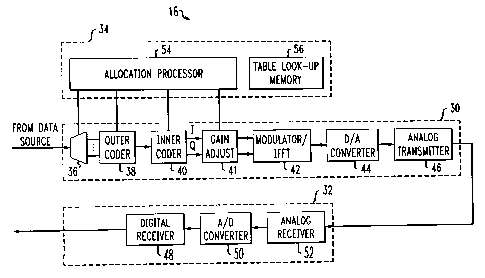
Fig. 2 shows in further detail an exemplary embodiment of the DSL modem 16 of
Fig. 1. In general, the DSL modem 16 includes a transmission path 30, a
reception path 32,
and a control unit 34. The transmission path 30 includes a demultiplexer 36,
an outer coder
38, an inner coder 40, a digital gain adjust 41, a modulator/IFFT block 42, a
digital to analog
CA 02399265 2002-11-29
8
("DJA") converter 44 and an analog transmitter 46. The reception path 32
includes a digital
receiver48~ an analog to digital ("A/D") converter 50 and an analog receiver
52. The
control unit 34 includes an allocation processor 54 and a table look-up memory
Sb.
In general, the demultiplexer 36, outer coder 38, inner coder 40, digital gain
adjust
41, modulator/IFFT block 42, and digital receiver 48 are functional blocks
that may be
embodied as operations within one or more digital signal processors or other
types of
processors. The allocation processor 54 represents a functional block that may
be executed
by a separate processor, or a processor shared with other functional blocks.
Accordingly, it
will be appreciated that the configuration of processing units employed to
carry out the
functions ascribed to the various functional blocks is not germane to the
invention. Those of
ordinary skill in the art may readily configure the processing circuit in a
manner that best
suits their implementation needs.
Referring specifically to the transmitter 30, the demultiplexer 36 is operably
coupled
to receive data to be transmitted, or payload data, from an external source
such as the user
1 ~ data source 12 of Fig. 1. The demultiplexer 36 is operable to demultiplex
or divide the
incoming data into a plurality of N parallel channels or bins. Each of the N
bins corresponds
to one of N carrier frequencies or tones, f, where i = 1-N. The demultiplexer
36 provides
the N demultiplexed data signals to the outer coder 38. To this end, the
demultiplexer 36
divides the incoming data to specific bins in accordance with control signals
provided by the
allocation processor 54.
As discussed above, the data in each bin is ultimately modulated onto one of
the
discrete tones or carrier frequencies f of the multitone signal. Accordingly,
the allocation of
the incoming data to the various bins of by the allocation processor 54 and
the multiplexer
36 effectively assigns the incoming data to the frequency channels or tones on
which it will
be modulated. As discussed further below, the allocation processor 54 provides
control
signals that allocates data to bins in a manner that improves the overall data
rateJtransmission power efficiency.
'The outer coder 38 is a forward error correction device that incorporates,
among
other things, parity symbols that are used for error correction on the receive
side. In general,
CA 02399265 2002-11-29
9
the outer codes 38 receives data bits for each of the N bins from the
multiplexes and
produces data blocks for each bin. Each data block includes the payload
symbols from the
multiplexes 36 and a number of panty symbols. Each payload symbol includes a
number of
payload bits, e.g. eight, while each parity symbol includes a number parity
bits, e.g. eight.
Thus, the output of the decoder may be characterized as having n bits total
output, k payload
bits, and n-k parity bits. It is known that if more parity symbols are used
per payload
symbol, then less power is required to achieve a desired bit error rate in
transmission. If
more power is used, then less parity symbols are required to achieve the same
bit error rate.
The forward error correction device may take many forms, but is a linear block
codes
in the embodiment described herein. A Reed-Solomon encoder is a nonlimiting
example of
a suitable linear block codes. In any event, the outer codes 38 is coupled to
receive control
or parameter signals from the allocation processor 54. Specifically, the outer
codes 38 is
configured to receive a control signal that specifies, for each bin, a number
representative of
the number of parity symbols per payload symbol. In accordance with one
embodiment of
the present invention, the allocation processor 54 adjusts the parity symbol
rate of the outer
codes 38 for one or more bins or channels f in order to increase the overall
transmission
efficiency.
The efficiency of the outer codes 38 may be illustrated by graphing the power
required to achieve a certain bit error rate as a function of parity symbol
density or rate. Fig.
3 includes such a graph. The y-axis of the graph indexes the transmit signal
to noise power
required to achieve a given bit error rate, while the x-axis of the graph
indexes the payload
bits per modulation symbol (which includes the total number of payload and
parity bits).
It is to be noted that the use of the term "symbol" in the context of Fig. 3,
as a
modulated symbol, is distinguished from the payload symbols and parity symbols
output by
the outer codes 38. In particular, as will be discussed further below, the
"symbols"
generated by the outer codes 38 are subsequently modulated into a series of
modulated
symbols, such as QAM symbols. Although each individual modulated symbol may or
may
not include parity bits and/or payload bits, the stream of modulated symbols
will include an
average number of payload bits per symbol, and a complementary average number
of parity
CA 02399265 2002-11-29
bits per symbol. Thus, one measure of the density of parity information is the
average
number of payload bits per modulated symbol. The graph of Fig. 3 employs that
measure as
its x-axis index.
As shown in the graph, for a given constellation size, the required signal to
noise
5 power increases as number of payload bits per modulated symbol increases.
For example,
reference is made to the QAM-1024 curve 60. A QAM-1024 symbol may have one of
1024
possible constellation positions or values. Because 1024 is equal to
2~°, each QAM-1024
symbol carnes ten bits worth of information. As illustrated in the graph of
Fig. 3, more
power is required as the number of payload bits per symbol moves toward ten.
At ten
10 payload bits per symbol, no parity symbols are present, and maximum power
is required.
It can be observed that the increase in power requirement is not linear. In
particular,
as shown, for example, by the 1024-QAM curve 60, the curve 60 moves from a low
slope
region 62 from five to eight bits per parity symbol to a high slope region 64
between nine to
ten bits per symbol. It can be seen that very little increase in power is
necessary to increase
the bits per symbol from six to seven. Accordingly, the outer coder 38 may not
be
optimized at six bits per symbol using 1024-QAM modulation because only a
small increase
in power yields a large effective data rate increase. Contrariwise, it can be
seen that
significantly more power is necessary to increase the bits per symbol from
nine to ten. As a
result, the outer coder 38 may not be optimized at ten bits per symbol using
1024-QAM
modulation because only a small decrease in data rate (i.e. from ten to nine
payload bits per
symbol) yields a significant power requirement reduction.
The efficiency of the outer coder 38 for a given modulation type may be
illustrated
by a graph showing the distance from the Shannon efficiency for the coder as a
function of
payload bits per symbol. The Shannon efficiency is a theoretical limit of
transmission
efficiency for a given channel. Thus, the distance from Shannon illustrates
how closely a
given channel is operating to its theoretical efficiency limit. Fig. 4
illustrates an exemplary
graph of curves showing the distance from Shannon efficiency as a function of
payload bits
per symbol for the same modulation types as those illustrated in Fig. 3.
Referring again by
way of example to the 1024-QAM curve 66, it can be seen that the outer coder
38 is
CA 02399265 2002-11-29
11
relatively inefficient at points below eight bits per symbol and at points
approaching ten bits
per symbol, which corresponds to the analysis of the curve 60 of Fig. 3
discussed above.
One aspect of the present invention which will become more readily apparent
below
in connection with the discussion of Figs. 7 and 8 is that power is allocated
between the
various bins in a manner that tends to push the efficiency of each channel
towards its nearest
point to the Shannon efficiency. By contrast, attempting merely to optimize
equal power
allocation among the channels, as provided by the prior art water pouring
algorithm, results
in channels operating at points that are not nearest their Shannon efficiency.
Referring again specifically to Fig. 2, the allocation processor 54 in
accordance with
i0 one aspect of the present invention attempts to coordinate the allocation
of bits between the
various bins and in such a way as to allow the outer coder 38 to use a parity
symbol rate for
each channel that causes the outer coder 38 to operate in a relatively
efficient portion of its
bits per symbol rate curve for the modulation rate. Such choice of parity
symbol rate will
depend on the noise and channel attenuation of each particular channel.
The inner coder 40 is an encoding device that generates encoded digital
signals
having I and Q vector values such as those ordinarily used to define positions
in quadrature
amplitude modulation ("QAM") signal constellation space. One of the primary
operating
parameters of the inner coder 40 is the constellation size employed by the
inner coder 40 to
encode a set of input signals. For example, the inner coder may employ
constellation sizes
that correspond to 4-QAM, 16-QAM, 64-QAM, 256-QAM and even larger QAM
constellation sizes. Larger constellation sizes provide a higher data rate,
but typically
require a greater signal to noise ratio to achieve an acceptable bit error
rate. (See, e.g., Fig.
3).
In the exemplary embodiment described herein, the inner coder 40 comprises a
trellis
coder that is operable to add overhead/parity information that increase the
effective bit error
rate of the signal, however at a cost of the additional overhead bits.
Nevertheless, it has
been found that overall efficiency of a DSL modem may be increased by
incorporating
trellis encoding.
CA 02399265 2002-11-29
12
Regardless of the actual design of the inner coder 40, the output of the inner
coder 40
may be characterized by the constellation size used to encode the input data
bits, regardless
of the amount of overhead added by the coder. Thus, the inner coder 40 is
operable to
receive data blocks for each of the N bins from the outer coder 38 and
produces encoded
signals having particular constellation size for each of the bins. If the
inner coder 40 is, for
example, a trellis encoder, then additional overhead bits are added. For
example, the trellis
inner coder 40 may produce for a particular bin a four bit constellation size
( 16-QAM) of
input bits plus trellis overhead.
It is noted, however, that the input bits to the inner coder 40 include both
payload
data and parity symbol overhead previously added by the outer coder 38. Thus,
the encoded
data signal produced by the inner coder 40 includes the payload data from the
multiplexer
36 as well as overhead added by the outer coder 38 and the inner coder 40.
As discussed above, the constellation size selected for each bin largely
defines the
effective data rate of the transmitted signal. For example, a 4096-QAM signal
has several
times the data rate of a 64-QAM signal. As mentioned above, the additional
data rate comes
at a cost of signal power, however. For example, the transmit signal to noise
ratio required
to send a 4096-QAM signal at a select bit error rate is much higher than the
signal to nose
ratio required to send a 64-QAM signal at that same bit error rate. As shown
in Fig. 3, the
curves for the higher constellation size signals tend to require increasingly
more power.
As a general matter, large constellation sizes are used in bins associated
with
transmission channels that have less noise and attenuation because such
channels may
support a larger signal to noise ratio with less transmission power. By
contrast, small
constellation sizes will be used in bins associated with transmission channels
that are noisier
andlor have more attenuation. As also shown in Fig. 3 and discussed above,
increasing the
outer coder parity symbol rate (i.e. reducing the payload bits per parity
symbol on the graph
of Fig. 3) tends to reduce the signal power requirement for a given
constellation size.
However, as more parity symbols are employed by the outer coder 38, less bits
of the actual
n-QAM constellation size are actually dedicated to payload bits, and the
effective data rate is
thus reduced.
CA 02399265 2002-11-29
13
The combination of the efficiency characteristics of the outer codes 38 and
the inner
codes 40 is therefore a multivariable function that is dependent upon the
parity symbol rate
yr density of the outer codes 38 and the constellation size employed by the
inner codes 40.
As discussed above, the allocation processor 54 adjusts the operation of the
outer codes 38
to improve the efficiency of the overall transmission by selecting the parity
symbol rate that
balances transmission power requirements and parity symbol overhead in an
advantageous
manner. Similarly, the allocation processor 54 adjusts the constellation size
of the inner
codes 40 to balance power requirements with overall data rate. To this end,
the allocation
processor 54 provides to the inner codes 40 parameter control information that
causes the
inner codes 40 to encode data signals for each of the N bins with a specific
constellation size
adjusted to suit the noise and attenuation characteristics present in the
channel.
The inner codes 40 is operably connected to provide encoded I,Q signals to the
gain
adjust block 41. The gain adjust block 41 is a device that adjusts the gain
for each of the N
bins in accordance with control signals provided by the allocation processor
54. In
particular, the allocation processor 54 determines the power required to
achieve a
predetermined bit error rate, given the chosen operating parameters of the
outer codes 38
and inner codes 40 for each channel, as part of its operations to improve
efficiency, as will
be discussed further below in connection with Fig. 5.
The gain adjust block 41 is operably connected to provide the gain adjusted,
I, Q
encoded digital signal to the modulator/IFFT block 42. The modulator/IFFT
block 42 is a
device or functional block that is operable to modulate the data from each of
the N bins onto
corresponding tones of the multitone signal. The modulator/IFFT 42 is further
operable to
transform the modulated signal into the time domain using an inverse fast
Fourier transform.
The resulting signal is the final digital output signal. The modulator/IFFT
block 42 is thus
operable to receive gain adjusted encoded digital signal from N bins and
generates a digital
time domain, modulated signal therefrom.
The modulator/IFFT 42 is operably coupled to provide the time domain output
signal
to the D/A converter 44. The D/A converter 44 is operable to convert the
digital signal to an
analog signal. The D/A converter 44 is operably coupled to provide the analog
signal to the
CA 02399265 2002-11-29
14
analog transmitter 46. The analog transmitter 46 is a circuit that is operable
to perform any
filtering, amplification and conditioning to the analog signal necessary to
facilitate
transmission of the analog output signal over the subscriber loop 20 (See Fig.
1 ). Such
circuits are well known in the art.
In general, the receiver path 32 is the analog of the transmitter path 30, and
the
details of its operation are not particularly germane to the exposition of the
present
invention. Nevertheless, in general, the analog receiver 52 receives analog
signals that
include digital, DMT-modulated information. The analog receiver 52 is a
circuit that is
operable to properly scale, filter and otherwise condition the received signal
for conversion
to a digital DMT-modulated signal. The analog receiver 52 is operably coupled
to provide
the received signal to the A/D converter 54. The A/D converter 54 converts the
received
and conditioned analog signal into a digital signal in the form of a time
domain, DMT-
modulated data signal. The A/D converter 54 is operably coupled to provide the
digital
signal to the digital receiver 48.
The digital receiver 48 includes the appropriate decoding, demodulating and
FFT
devices or functions that are necessary to convert the time domain, DMT-
modulated data
signal into a digital data baseband signal. As discussed above the digital
receiver 48
contains the analog to the coders 38, 40 and modulator/IFFT 42 of the
transmission path 30.
The allocation processor 54 is a processing device, or a functional portion of
a
processing device or circuit, that is operable to control the allocation of
data bits to each of
the N bins, control the allocation of power to each of the N bins, and control
operational
parameters of the outer coder 38 and inner coder 40. The allocation processor
54 controls
such elements in an accordance with methods of the invention to reduce the
amount of
power required to transmit at a given data rate having a given bit error rate.
To this end, the
allocation processor 54 performs the operations describe below in connection
with Fig. 6.
The allocation processor 54 is operably connected to the table look up memory
56 to obtain
configuration data pertaining to the transmission path 30.
In particular, the table look up memory 56 contains a table of data that
identifies, for
a given desired bit error rate, a value representative of the transmission
signal to noise ratio
CA 02399265 2002-11-29
required to achieve a particular payload data transmission rate. The payload
data
transmission rate in the abstract is defined by the constellation size of the
inner coder 40,
less the parity bits added by the outer coder 38. Thus, each record on the
table is associated
with the encoder parameter values that are required to achieve the payload
transmission data
S rate.
In particular, as used herein, each table entry is defined by its associated
parameter
settings (a, b), where a is a value representative of the parity byte density
of the outer coder
38 and b is a value representative of the constellation size of the inner
coder 40. The
associated data rate k for each table entry (a, b) may be derived as a
function of a,b, as
10 discussed further above. The signal to noise power SNR(a, b) required to
transmit at the rate
k defined by the parameters (a, b) is stored in connection with the table
entry (a, b).
The table entries (a, b) are stored as an ordered table e~ztry list, in which
the table
entries are stored in ascending SNR(a, b) values, i.e. ascending signal to
noise power
requirement values. Moreover, the table entries are also stored in ascending
data rate values
15 k, which is a function of (a, b). Thus, movement up the list identifies a
set of parameters
settings (a, b) that have a higher data rate k and a higher signal to noise
requirement SNR(a,
b), while movement down the list identifies a set of parameter settings (a, b)
that have a
lower data rate k and a lower signal to noise requirement SNR(a, b).
The allocation processor 54 employs the table entry list in the memory 56 to
determine appropriate parameters for the outer coder 38 and inner coder 40 in
the allocation
of transmission power to each of the N bins. In doing so, the allocation
processor 54 further
employs the table entry list to determine efficient allocation of input bits
and transmission
power to each of the bins as described below in connection with Figs. 7 and 8.
In essence,
the allocation processor 54 attempts to cause each channel to operate at or
near its most
efficient point, for example, the point nearest its Shannon efficiency for a
given data rate.
(See Fig. 4). Fig. 5 shows an exemplary set of operations that are used to
configure the
table entry list in the memory 56. As an initial matter, in step 102, a bit
error rate is selected
for the table entry list. Then, in step 104, an a x b matrix is defined that
is indexed by a set
of a possible parity symbol rate settings for the outer coder 38 and a set of
b possible input
CA 02399265 2002-11-29
16
bit constellation sizes for the inner coder 40. Each point (a, b) in the
matrix represents an
effective transmission data rate. As discussed above, the effective data rate
may be
calculated from the parameters (a, b) essentially from subtracting the parity
symbol bits
defined by a from the constellation size defined by b. The derived data rate
may optionally
be stored for each matrix position. However, it will be appreciated that even
if the actual
data rate is not stored, the information sufficient to calculate the effective
data rata may
readily be calculated for each matrix position (a, b).
In step 106, the a x b matrix is populated with transmission signal to noise
requirements, SNR(a, b), required to transmit each bit reliably at the
predetermined bit error
rate using the parameters (a, b). To this end, tests may be conducted for each
point (a, b) of
the matrix in which the transmission power is varied over a range in a known
noise
environment until the desired bit error rate is achieved.
Once the signal to noise requirement SNR(a, b) for each point (a, b) of the
matrix is
identified, the matrix is sorted into a preliminary table entry list in step
108. Similar to the
table entry list discussed above, the preliminary table entry list is in an
order that ascends
from the least effective data rate value to the highest effective data rate
value. Thus, for
example, from any particular position on the list, the next highest position
will have a higher
effective data rate and the next lowest position will have a lower effective
data rate. As with
the matrix, each point on the list is indexed by its (a, b) parameters and
contains a required
signal to noise value SNR(a, b).
Unlike the table entry list, the preliminary table entry list is not
necessarily in
ascending order with respect to the required signal to noise value SNR(a, b).
In other words,
because some configurations a, b of the coders 38, 40 are relatively
inefficient, even low
data rates can require a relatively high signal to noise requirement. In step
110, these
inefficient points are removed from the list. To this end, the preliminary
table entry list is
ascended from the least data rate point to the highest data rate point. During
this ascending
operation, any point (a, b)~ in which the signal to noise requirement SNR(a,
b)~ is higher than
that of the next highest point, (a, b)~+1, is removed. In other words, if for
any point (a, b)~:
SNR(a, b)~ > SNR(a, b)~+~, then the point (a, b)~ is removed from the table
entry list. The
CA 02399265 2002-11-29
17
point is (a, b)l is removed because its parameter configuration would never be
used, since
one may achieve a higher data rate (i.e. at (a, b)1+O while using less power
simply by
employing the {a, b)~+i parameter configuration.
The entire preliminary table entry list is scanned until all such points are
removed.
The resulting list is the table entry list. The table entry list comprises a
list of parameter
configurations (a, b) that are monotonically ascending in both effective data
rate and signal
to noise power requirement values. In step 112, the final table entry list is
stored in the table
look-up memory 56 of the DSL modem 10.
The configuration of the table entry list described above in connection with
Fig. 5
may preferably occur prior to use of the DSL modem 10. Fig. 6, by contrast,
shows the
operations of the DSL modem 10 during the course of an ordinary communication
operation. Fig. 6 will be described with simultaneous reference to Figs. 1 and
2.
First, in step 202, a connection is established with the receiver of the DSL
modem
signals. In the exemplary embodiment shown in Fig. 1, the receiver is the
DSLAM 26,
which can then transmit the signal over the Internet 18 to the final
destination.
Thereafter, in step 204, the allocation processor 54 causes a test signal to
be
transmitted to the receiver. The test signal is preferably a pseudorandom
noise signal having
known content. The receiver, i.e. the DSLAM 26, compares the received signal
with its
known content in order to obtain the channel transfer function H(~, where f
may suitably be
the frequency of each tone of the multitone signal on which data may be
modulated, The
DSLAM 26 also measures the channel noise power N(~ by measuring the channels f
while
the transmitter is silent. The allocation processor 54 obtains these values
and calculates the
ratio of noise power to channel attenuation NH(f) = N(f)l~H(f)~z. The ratio
NH(f) represents a
measure of the noise power and attenuation that the transmitted signal is
required to
overcome to ensure detection at the receiver. The allocation processor 54
stores the NH(f )
values for each channel f locally.
Thereafter, in step 206, the allocation processor 54 performs an initial
allocation of
power and bits to each bin or channel f of the multitone signal. The initial
allocation is
based on a substantially even distribution of signal power over the channels,
with some local
CA 02399265 2002-11-29
18
optimization. In practice, the initial allocation may suitably be any water
pouring type
algorithm, such as those known in the art. Fig. 7, described below,
illustrates in further
detail an exemplary initial allocation procedure that may be used in step 206.
In accordance with one aspect of the present invention, the initial allocation
performs
its optimization step by selecting various combinations of parameters of both
the outer coder
38 and inner coder 40. In other words, the initial allocation does not merely
adjust the
operation of either the outer coder 38 or inner coder 40 alone, but selects
from combinations
of various settings for each coder, thereby increasing the potential
efficiency of the initial
allocation.
At the end of step 206, the allocation processor 54 has defined an initial
transmit
power allocation, P(f ), and an initial bit rate allocation, k(f ), for each
channel f . In general,
the values of P(f ) and k(f ) for each channel correspond to a point (a, b) in
the table entry list
stored in the table look-up memory 56, and thus has associated with it a set
of coder
parameters, a, b. In particular, during the initial allocation of step 206,
the allocation
processor 54 selects an appropriate initial table entry list point (a, U); for
each channel f .
The bit rate associated with the parameters (a, b); for that entry represents
the initial bit
allocation rate k(f ) and the required signal to noise value SNR(a, b); is
used to derive the
initial transmit power P(f;). The initial transmit power P(f ) is set equal to
the amount of
power required to achieve the required signal to noise SNR(a, b); over the
channel f,~, given
the noise and attenuation characteristics NH(f ) for the channel.
After initial allocation, the allocation processor 54 begins an iterative
incremental
reallocation process described below in connection with steps 208-210. In step
208, the
allocation processor 54 removes increments of power from one or more channels
f in which
a relatively small decrease in data rate k(f ) results in a relatively large
decrease in power
P(f ). To this end, the allocation processor 54 finds alternative points (a,
b)"; on the table
entry list for the one or more channels using the table look-up memory 56,
wherein the
alternative points (a, b)"; provide a change in effective data rate k(f ) that
is relatively small
compared to the amount of decrease in the SNR(a, b);. The newly found list
entries define
CA 02399265 2002-11-29
19
the new k(f ) and P(f ) allocation for the affected channels) f . The power
that is removed
from these channels is excess power that may be reallocated in step 210.
In step 210, the allocation processor 54 reallocates the excess power to one
or more
other channels f in which a relatively small increment in power P(f ) results
in a relatively
large increase in data rate k(f). To this end, the allocation processor 54
finds alternative list
entries (a, b)m; from the table look-up memory 56 in which the change in
effective data rate
k(f ) is relatively large compared to the amount of increase in the SNR(a,
b);. The newly
found list entries define the new k(f ) and P(f ) allocation for those
affected channels) f . In
this manner, power is reallocated into channels in which it is used more
efficiently.
After step 210, the allocation processor 54 has an improved allocation of
power P(f;)
and bit rate k(fi) for the various channels f of the multitone signal. Further
details regarding
steps 208 and 210 are provided below in connection with Fig. 8. After step
210, the
allocation processor 54 may configure the DSL modem 10 for operation. To this
end, the
allocation processor 54 proceeds to step 212.
In step 212, the allocation processor 54 then controls the operation of the
multiplexes
36, the outer codes 38, the inner codes 40, and the gain adjust block 41
accordingly. In
particular, the allocation processor 54 controls the multiplexes 36 to
allocate bits to each bin
f in accordance with the data rate k(f ) as defined by the corresponding table
list entry (a, U);
employed for each bin. The allocation processor 54 then provides control
signals that cause
the outer codes 38 to use the amount of parity symbols that correspond to the
value of a
corresponding to the table list entry (a, b); for each channel f. Similarly,
The allocation
processor 54 then provides control signals that cause the inner codes 40 to
use the
constellation size that corresponds to the value of b corresponding to the
table list entry (a,
b); for each channel f . The allocation processor 54 furthermore controls the
gain adjust
block 41 such that the gain for each channel f, corresponds to its P(f )
value.
So configured, the DSL modem 10 may begin to transmit data received from the
data
source 12. The received digital data is multiplexed into the N bins (f where i
= 1 to 1~ by
the multiplexes 36. As discussed above, the allocation processor 54 controls
the multiplexes
36 to effect the proper allocation of bits to the various bins. The
multiplexes 36 provides the
CA 02399265 2002-11-29
multiplexed digital data to the outer coder 38. The outer coder 38 codes the
data of each bin
f" adding parity symbols at a rate defined by the a parameter for the table
entry (a, b);
selected for the corresponding bin f . The outer coder 38 provides the coded
signal to the
inner coder 40. The inner coder 40 likewise codes the data of each bin f ,
adding overhead
5 information and using a constellation size defined by the b parameter for
the table entry (a,
b); selected for the corresponding bin f . The inner coder 40 then provides
the encoded
digital data, typically as an l, Q vector value, to the gain adjust block 41.
The gain adjust block 41 individually adjusts the gain for each bin f in
accordance
with the P(f;) value provided by the allocation processor 54. The gain adjust
block 41
10 provides the gain adjusted, encoded signal to the modulator/IFFT block 42.
The
modulator/IFFT block 42 modulates the signal for each bin onto its selected
tone frequency
f and then performs an inverse fast Fourier transform to generate a time
domain signal. The
resulting signal is provided the D/A converter 44 and thereafter to the analog
transmitter 46.
The analog transmitter 46 conditions and transmits the signal over the
subscriber
15 loop 20. The signal propagates through the loop transmission facility 22 to
the central office
24. The central office 24 switches the signal to the DSLAM 26. The DSLAM 26
receives
the signal and obtains the data therefrom. The DSLAM 26 may then transmit the
data signal
over the Internet 18 to one or more receiving computers 14.
Fig. 7 shows an exemplary initial allocation algorithm that may be employed by
the
20 allocation processor 54 or another processing circuit in a mufti-frequency
communication
device. The operations of Fig. 7 may suitably be used as the initial
allocation step 206 of
1 lg. 6. In general, the initial allocation algorithm of Fig. 7 begins by
allocating much more
power than is available to each channel and then removes power from all of the
channels
until the allocated power is equal to the actual available power.
2~ As an initial matter, several variables are initialized. Specifically, in
step 302, the
allocation processor 54 sets P,or equal to the total power that is actually
available for the
transmission, sets P target = MAX, and sets P_step = 1Ø P target represents
the amount
available to be allocated to each channel or bin during each iteration of the
algorithm. The
value MAX is a large initial value that represents much more power than each
channel could
CA 02399265 2002-11-29
21
possibly be allocated. Thus, in other words, MAX * N is greater than P,ot,
where N is equal
to the number of channels. P step is the value of power removed from each
channel during
each iteration of step 304, discussed below.
After initialization of variables in step 302, the allocation processor 54
proceeds to
step 304. In step 304, the allocation processor 54 decreases the available per
bin power
P_target by the value of P_step. Thereafter, the allocation processor 54
determines the per
bin power allocation P(f;) based on the highest data rate that is sustainable
on each channel f
using P_target. Because P_target typically does not correspond exactly to the
highest
achievable data rate, P(f ) will typically be less than P target.
Specifically, the maximum data rate achievable given a value P_tai get may be
determined by identifying the maximum signal to noise ratio SNR_target(f )
available for
each channel f . The maximum signal to noise ratio is determined by taking the
power
available, P_target, and dividing the available power by the measure of noise
and
attenuation for the channel, given by NH(f ). Thus, the maximum available
signal to noise
ratio, SNR_target(f) is given by
SNR_target( f ) = P_ta~ getlNH(f )
Thereafter, the allocation processor 54 determines, for each channel, the
table entry (a, b)
having the highest signal noise requirement SNR(a, b) that is less than or
equal to
SNR_target(f ). That point represents the highest sustainable data rate k(f ),
because the next
highest point on the table (with a higher data rate) requires more signal to
noise power than
is available for the channel f.
Typically, no table entry (a, b) has an SNR(a, b) value that is exactly the
same as the
available signal to noise value SNR_target(f ) for a given channel, due to the
quantization
steps between entries on the table entry list. As a consequence, the
SNR_target(f) will
usually fall between two adjacent SNR(a, b) values on the table. The lower of
the two
adjacent SNR(a, b) values represents the maximum sustainable data rate, given
the
SNR_target(f ) value. The SNR(a, b) corresponding to that point on the table
entry list
becomes the transmit SNR of the channel, or SNRx",;,(f ). The difference
between SNR,,.""r(.f )
CA 02399265 2002-11-29
22
and SNR_target(f ) is representative of the excess power (normalized for the
channel f )
because that additional power does not increase the bit rate that may be
supported.
After the transmit SNR, SNRx",;,(f ), of the channel f is determined, the
allocation
processor 54 determines the actual power required to achieve the SNRxm;~(f;).
The actual
power required to be transmitted, P(f ) is obtained by factoring in the noise
and attenuation
characteristics of the channel:
P(f ) = SNR,x",;,(f ) * NH( f )
Thus, the allocation processor 54 in step 304 postulates a power allocation
that
eliminates unused excess power from each channel. The allocation processor 54
then
calculates the sum of the transmit power allocations to all channels f, given
by
Total Power = E P(f ), for i = 1 to N
In step 306, the allocation processor determines whether the total power
allocated,
Total_Power, is greater than the actual available power, P,or. If so, then
more power will
have to be removed from the per channel power allocations P(f ) by repeating
step 304.
Accordingly, if Total_Power > P,o,, then the allocation processor 54 returns
to step 304 to
remove more power from the per channel available power allocation P target and
to
determine new P(f ) values based thereon.
However, if in step 306 it is determined that Total Power is not greater than
P,or,
then the allocation processor 54 executes step 308. It will be appreciated
that at step 308,
the power allocations P(f ) are potentially viable because their total (Total
Power) is equal
to or less than the actual available power Pro,. Although the allocation is
viable, it may not
be very efficient. Accordingly, in step 308, the allocation processor 54
determines whether
the allocation of power is efficient enough to end the initial power
allocation algorithm. If
so, then the initial allocation is complete and the allocation processor 54
proceeds to step
314. If not, then the initial allocation will continue and the allocation
processor 54 executes
step 310.
The determination of whether the allocation of power is efficient enough in
step 308
may be made a number of ways. For example, the allocation processor 54 may
determine
whether the difference between the total power used and the actual available
power is less
CA 02399265 2002-11-29
23
than a threshold. For example, the allocation processor 54 may determine
whether (Pro, -
Total Power) < Prhresh~ In the alternative, the allocation processor 54 may
simply determine
whether P_step is less than a threshold. In particular, as will be discussed
below, each
iteration of step 310 results in the reduction of the value of P step. It is
noted that below
some level, additional reduction of P step will yield little or no improvement
in the
allocation of power among the channels or bins. Accordingly, the allocation
processor 54 in
step 308 may simply determine whether P step is less than a predetermined
level.
In any event, as discussed above, step 310 is executed if the answer in step
308 is in
the negative, or in other words, if it is determined that the initial
allocation is not complete.
In step 310, the allocation processor 54 adds back P step to the existing
P_ta~ get value, and
then reduces P_step to 1/10'h of its value. The allocation processor 54
thereafter returns to
step 304.
These operations of step 310 effectively reverse the most recent decrease in
P_tarRet
and then allow much smaller increments of P step to be removed from the P
target value in
ensuing iterations of step 304. The sum effect of steps 304-310 is that
progressively beer
changes of power allocation are used until a limit in resolution is reached,
as determined by
step 308.
As discussed above, the allocation processor 54 executes step 314 if the
answer in
step 308 is in the affirmative. In step 314, the initial allocation is
complete for the set of N
bins. Each bin f is associated with a table entry (a, b);, and thus has a
defined power signal
to noise requirement SNR(a, b);, a transmit power requirement P(f ) = SNR(a,
b); * NH(f ),
and a data rate k;, which is a function of a and b of (a, b);.
Fig. 8 shows a flow diagram of an exemplary embodiment of the subsequent
reallocation process of the present invention. Fig. 8 reallocates power to the
bins, using the
initial allocation described above in connection with Fig. 7 as a starting
point. However, it
will be appreciated that the operations of Fig. 8 may be used to efficiently
reallocate power
even if other initial power allocations are employed. The operations of Fig. 8
may suitably
be used to carry out steps 208 and 210 of Fig. 6.
CA 02399265 2005-06-O1
24
In step 402, the allocation processor 54 finds a maximum of the rate of
change,
dP(f ydk;, for all possible reductions in power for every bin. The rate of
change dP(f ydk;
may be defined as:
dP(f~~i - (P(ft, Clerrtltt(C,b))- PV', prOpo3td(a,b))l't ki, eurrentta~b) '
ki,proposed(a,b))
To this end, for each bin f, the difference between u'~e power required to
satisfy the existing
table entry (a, b); and that of each table entry having a lower SNR(a, b) is
calculated. Also,
the difference between the effective data rate k; of (a, b); and that of each
table entry having a
lower SNR(a, b) is calculated. The table entry (a, b),~ for which the change
in power
required dP(f ) divided by the change in data rate dk; is maximized
constitutes the maximum
dP(f ~dk; point for that bin f . Moreover, the allocation processor 54
determines the
frequency bin f ,"~ that has the maximum dP(f )ldk; for all bins. Once the
maximum
dP(f )ldk; for f,",~ is identified, then the allocation processor 54 proceeds
to step 404.
In step 404, the allocation processor 54 changes the table entry (a, b); for
the
frequency f ,",~ to the table entry (a, b)";, at which point the dP(f )ldk;
value is maximized.
1~ As a result, the power allocated to f,",~, P(f,,"~ ) is reduced to SNR(a,
b)"; * NH(f,",a,r ), and
the data rate k;,,"~ is reduced to that corresponding to the settings (a,
b)";. The difference
between the previous power allocation and the new power allocation is added to
P,~,". The
result of the change is that relatively little effective data rate is lost in
f,",~, but a relatively
large amount of power has been reclaimed for reallocation.
Thereafter, in. step 406, the allocation processor 54 determines whether the
remainder
power P,t", is greater than another predetermined threshold P,t,~ rhrtsn2. If
not, then the
allocation processor 54 returns to step 402 to find another bin in which the
data rate may be
reduced to obtain additional power savings. If, however, in step 406 it is
determined that the
remainder power P,t", is greater than a predetermined threshold Pre",,
tl"YS,,z, then the
allocation processor proceeds to step 408 to reallocate the accumulated excess
power P,tm.
Alternatively, in step 406, the allocation processor 54 may simply determined
whether step 402 has been executed a predetermined number of times. 1f not,
then the
allocation processor 54 would return to step 402. If so, then the allocation
processor 54
would execute step 408.
CA 02399265 2005-06-O1
In any event, in step 408, the allocation processor 54 fords a minimum of the
rate of
change, dP(f )/dk;, for all possible increases in power for every bin. The
rate of change
dP(f ydk; is still deftned as:
dP(f )ldk; = (P~. Currrnt(a.b))' P~. P~Pos~~a.b ~ )~(kf. current(n.b) '
ki.proposedl0.6))
5 However, unlike step 402, for each bin f, the difference between the power
required to
satisfy the existing table entry (a, b); and that of each table entry having a
higher SNR(a, U)
is calculated. Also, the difference between the,effective data rate k; of (a,
U); and that of
each table entry having a higher SNR(a, b) is calculated. The table entry (a,
b)",; for which
the change in power required dP(f ) divided by the change in data rate dk; is
minimized
10 constitutes the minimum dP(f )ldk; point for that bin f . Moreover, the
allocation processor
34 determines the frequency bin f.",;" that has the minimum dP(f)ldk;. Once
the nunimum
dP{f ~dk; for f.""" is identified, then the allocation processor 54 proceeds
to step 410.
In step 410, the allocation processor 54 changes the table entry (a, b); for
the
frequency f .,";" to the table entry (a, b),";, at which point the dP( f;~dk;
value is minimized.
15 As a result, the power allocated to f,",;", P(f.m;") is increased to SNR(a,
b)",; * NH(f,",;"), and
the data rate k;,",;" is increased to that which corresponds to the settings
(a, b)",;. The
difference between the previous power allocation and the new power allocation
is subtracted
from Pram. The result of the change is that a relatively large effective data
rate increase is
obtained, and a relatively small amount of power has been reallocated from the
Pre",.
20 Thereafter, in step 412, the allocation processor 54 determines whether the
remainder power Prcm is less than the predetermined threshold Pre~n, thresh2~
If not, then more
power may be reallocated and the allocation processor returns to step 408 to
find another bin
in which a relatively small amount of power may be reallocated from Pr~",
while obtaining a
relatively large data rate increase. If however, Pre," is less than the
predetermined threshold
Pr~, thresh2, then the allocation processor 54 proceeds to step 414.
In step 414, the allocation processor 54 determines whether the power
allocation to
the N bins has changed from the allocation that existed prior to the last
execution of step 402
(i.e. after both the add and remove iterations of steps 404 and 410). If not,
then the
algorithm has converged and additional iterations will not result in any
different power
CA 02399265 2002-11-29
26
allocation. In such a case, the allocation processor 54 may stop the
operations of Fig, 8 and
begin controlling the DSL modem 10 in accordance with the final allocations,
as described
above in connection with step 112 of Fig. 6. If, however, the power allocation
to any of the
Nbins has changed during the last iteration, however, then the allocation
processor 54
3 returns to step 402 to execute another reallocation iteration.
The above described embodiments are merely illustrative, and those of ordinary
skill
in the art may readily devise their own implementations that incorporate the
principles of the
present invention and fall within the spirit and scope thereof.