Note: Descriptions are shown in the official language in which they were submitted.
CA 02399427 2002-08-06
Specification
SEMICONDUCTOR LASER MODULE
Technical Field
The present invention relates to a semiconductor laser
module having the function of controlling the temperature of
a semiconductor laser.
Background Art
As a semiconductor laser module having the function of
coiztrolling the temperature of a semiconductor laser, there
is a known unit described in FLD5F14CN-E19 to E58 of FUJITSU
SEMICONDUCTOR DEVICE DATA SHEET (DS02-12601-2). The automatic
temperature control circuit described in the DATA SHEET has
a Peltier element and a thermistor contained in a laser diode
and an analog integrator and used for temperature control by
proportion~integration (P. I) control so that the actual
temperature conforms to a set temperature.
Absolute precision and absolute stability of wavelength
are required in the wavelength division multiplexing (WDM)
communication system. Although distribution feedback (DFB)
type semiconductor lasers are employed in such a WDM communication
system, the temperature of the laser at the time of oscillation
needs controlling precisely because the oscillation wavelength
1
CA 02399427 2002-08-06
of the DFB type laser is easily affected by the temperature
of the laser. The oscillation wavelength between adjoining
channels tends to be set at 0 . 8 nm or less in the WDM communication
system in recent years. The required wavelength precision of
the laser for use in the system like this is 0.01 nm. In order
to attain these requirements, it is needed to control the
temperature of the laser at the time of oscillation within 0. 1
°C .
In the above-described prior-art automatic temperature
control circuit, a steady state may be brought about in a state
that the actual temperature deviates from a set temperature
under the influence of thermal resistance and the like. In
order to increase the precision of the temperature control by
reducing the deviation between the actual temperature and'the
set temperature, the loop gainof a control systemneeds Increasing.
In the automatic temperature control circuit having a closed
loop using the Pettier element, however, though it is possible
to freely set a temperature in the case of PI control through
digital processing, there occurs a great delay in transmission
besides the primary delay between the Pettier element and the
thermistor in the case of analog processing as the system is
generally such that the response of the temperature is extremely
slow in comparison with the response of the electronic circuit .
For this reason, oscillation is likely to arise when the loop
gain of the control system is increased too much. Therefore,
2
CA 02399427 2002-08-06
the loop gain cannot be increased immoderately and this makes
it difficult to raise the precision of the temperature control.
An object of the present invention is to provide a
semiconductor laser module for making precise temperature
control possible.
Disclosure of the Invention
As a result of studies made earnestly on the foregoing
problems, the present inventors have found that when input to
an electronic refrigeration element is varied stepwise in the
steady state in controlling the temperature of a semiconductor
laser module using the electronic refrigeration element (a
Peltier element) and a temperature detection element, a delay
a:~_ises from a point of time when the input thereto is varied
until the output of the temperature detection. element begins
to actually vary and the delay greatly contributes to the
oscillation as well as the primary delay. An object of the
present invention is to cancel the delay.
Morespecifically, asemiconductorlaser moduleaccording
to the invention comprises: a semiconductor laser, laser
temperature control means having an electronic refrigeration
portion and a temperature detection portion for detecting
the temperature of the electronic refrigeration portion and
used for controlling the temperature of the semiconductor
laser, and control signal generating means for inputting a
3
CA 02399427 2002-08-06
detection signal of the temperature detection portion,
generating a control signal for conforming the temperature
of the electronic refrigeration portion with a set temperature
and sending the control signal to the electric refrigeration
portion, wherein the control signal generating means generates
a compensating signal for compensating for a delay of temperature
variation of the electronic refrigeration portion with respect
to an input of the control signal to the electronic refrigeration
portion, and generates a detection correction signal provided
by correcting the detection signal by the compensating signal
so as to generate the control signal according to the detection
correction signal and a signal corresponding to the set
temperature.
The provision of the control signal generating.means makes
it' possible to obtain the detection correction .signal which
reduce the delay of actual temperature variation with respect
to the set temperature variation as the detection signal is
compensated by the compensating signal even though the actual
temperature variation with respect to the set temperature
variation is detected by the temperature detection portion with
some delay caused by a delay in response between the electronic
refrigeration portion and the temperature detection portion.
The control signal is generated according to the detection
correction signal and the signal corresponding to the set
temperature and then inputted to the electric refrigeration
4
CA 02399427 2002-08-06
portion. Therefore, application of energy more than necessary
is prevented from being given to the electronic refrigeration
portion immediately after the set temperature in the steady
state is changed. As the loop gain of the control system can
be increased thereby, the actual temperature of the electronic
refrigeration portion is prevented from deviating from the set
temperature in the steady state. Therefore, the electronic
refrigeration portion can be put under precise temperature
control.
Preferably, the control signal gene rating means has a filter
circuit for inputting the control signal and generating the
compensating signal, and an addition circuit for adding the
detection signal and the compensating signal to generate the
detection. correction signal. Thus, rnean~s for generating the
comperis~atirig signal and means far generating the detection.
correction signal are attainable with a simple circuit
configuration. In the feedback loop in this ease, the whole
system is made controllable in an optimum mode by setting the
values of resistors and capacitors constituting the filter
circuit so that they have a filter time constant and a feedback
quantity as desired.
In this case, preferably the control signal generating
means has a first operational amplifier having one input portion
to which the detection signal is input and the other input
portion to which the control signal is input via a f first capacitor,
CA 02399427 2002-08-06
and a second capacitor and a resistor connected in parallel
between the other input portion and an output portion of the
first operational amplifier, and the first operational
amplifier, the first capacitor, the second capacitor, and
the resistor make up the filter circuit and the addition circuit .
In this case, the number of operational amplifiers used with
the filter circuit and the addition circuit may be one, so
that the circuit configuration of the module is simplified.
At this time, preferably the control signal generating
means further has a second operational amplifier having an
output portion connected to the other input portion of the
first operational amplifier via the first capacitor, and a
third capacitor connected between the output portion and one
input portion of the second operational amplifier, and the ,
third.. capacitor 'forms a part of the filter circuit: In thus
case, the number of capacitors serving the function as a low-pass
filter becomes two, so that two small-sized capacitors can
be appropriately combined to form a compensating signal having
any desired time constant.
Brief Description of the Drawings
FIG. 1 is a configuration diagram to show a first embodiment
of a semiconductor laser module according to the invention.
FIG. 2 is a diagram to show a specific circuit configuration
of the semiconductor laser module shown in FIG. 1.
6
CA 02399427 2002-08-06
FIG. 3 is operation wave form charts of the semiconductor
laser module shown in FIG. 1; (a) is an operation waveform
chart of set temperature; (b) is an operation waveform chart
of the output value of a bias circuit; (c) is an operation
wave form chart of the output value of a parallel compensating
circuit; and (d) is an operation wave form chart of the output
value of an addition circuit.
FIG. 4 is a diagram to show the circuit configuration
of a general semiconductor laser module in a prior art.
FIG. 5 shows comparison of current signals.applied to
Peltier elements; (a) is a drawing to show the current signal
of the semiconductor laser module shown in FIG: 4 and (b)
is a drawing to show the current signal of the semiconductor
laser mo.duie:shown in FIG. 1.
. FIG..6 is a diagram to show the circuit configuration
of a second embodiment of a semiconductor laser module according
to the invention.
Reference numerals in the figures are as follows : Numeral
1 denotes a semiconductor laser module, numeral 2 denotes
a semiconductor laser, numeral 3 denotes a laser temperature
control element portion (laser temperature control means),
numeral 4 denotes a Peltier element (electric refrigeration
portion),numeral5denotesathermistor(temperaturedetection
portion), numeral 6 denotes a differential amplification
circuit, numeral 7 denotes a bias circuit, numeral 9 denotes
CA 02399427 2002-08-06
an addition circuit, numeral 12 denotes a parallel compensating
circuit, numeral 21 denotes a high-pass filter circuit portion
(filter circuit) , numeral 22 denotes a low-pass filter circuit
portion (filter circuit), numeral 46 denotes an operational
amplifier(second operational amplifier), numeral 70 denotes
a semiconductor laser module, numeral 71 denotes a differential
amplification circuit, numeral 72 denotes a capacitor (third
capacitor) , numeral 73 denotes an operational amplifier (first
operational amplifier) , numeral 74 denotes a capacitor (first
capacitor.), numeral 76 denotes a resistor, and numeral 77
denotes a capacitor (second capacitor)._
Best Mode for Carrying Out the Invention
A description of a semiconductor laser module as the
preferred embodiments of the present invention will nowbe given
by reference to the drawings.
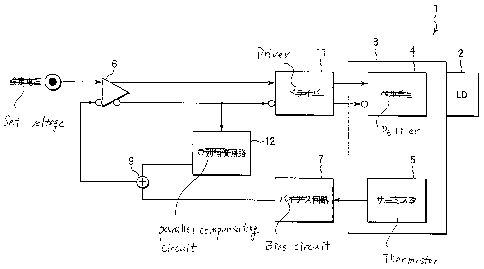
Fig. 1 is a configuration diagram to show a first embodiment
of a semiconductor laser module according to the invention.
As shown in the figure, a semiconductor laser module 1 according
to this embodiment is provided with a semiconductor laser (laser
diode) 2 and a laser temperature control element portion 3 for
controlling the temperature of the semiconductor laser 2. The
laser temperature control element portion 3 has a Pettier element
4 as an electronic refrigeration element and a thermistor 5
as a temperature detection element for detecting the surface
8
CA 02399427 2002-08-06
temperature of the Peltier element 4. In this case, the
semiconductor laser 2 and the laser temperature control element
portion 3 are in the form of, for example, one packaged integrated
circuit.
The semiconductor laser module 1 has a differential
amplification circuit 6 and a set signal (voltage) corresponding
to a set temperature (target temperature) of the surface of
the Pettier element 4 is applied to the non-inverting- (+) -side
input portion of the differential amplification circuit 6.
The thermistor 5 is connected to the inverting-(-).-side input
portion of the differential amplification circuit 6 via an
addition circuit 9 and a bias circuit 7. The non-inverting-side
output portion and the inverting-side output portions of the
different~.al amplification circuit 6 are connected via a driver.
11 t.o 'the two. metal electrodes (not shown) of the Pettier elerment
4. The differential amplification circuit 6 like this compares
the input voltage of non-inverting-side input portion with the
input voltage of inverting-side input portion and amplifies
a signal corresponding to the difference between the input
voltages with a predetermined amplifying degree (gain) to
generate the control signal (voltage). Then the output voltage
of the differential amplification circuit 6 is converted by
the driver 11 into a current signal and introduced into the
Pettier element 4.
The Pettier element 4, the thermistor 5, the bias circuit
9
CA 02399427 2002-08-06
7, the addition circuit 9, the differential amplification circuit
6 and the driver 11 constitute a feedback control system as
one closed loop in order to control the temperature such that
the surface temperature of the Peltier element 4 conforms to
the set temperature. In this case, the surface temperature
of the Peltier element 4 lowers as the current value input to
the Peltier element 4 increases, whereas the surface temperature
of the Peltier element 4 rises as the current value input to
the Peltier element 4 decreases.
A parallel compensating circuit 12 branches and is
connected to the inverting-side output portion of the
differential amplification circuit 6. The parallel
compensating circuit 12 generates a compensating signal for
compensating f.or a .delay.of temperature variation of the Peltier
element 4 withwrespect to input of a current signal to the.
Peltier element 4. The compensating signal is a signal with
direct current (DC) component cut (see FIG. 3 (c} ) . The output.
signal of the parallel compensating circuit 12 is input to
the addition circuit 9, forming a local loop. The addition
circuit 9 adds the output signal of the bias circuit 7
corresponding to the detection signal of the thermistor S
and the output signal of the parallel compensating circuit
12 to generate a detection correction signal (see FIG. 3 (d) ) .
Here, the differential amplification circuit 6, the bias
circuit 7, the parallel compensating circuit 12, and the addition
CA 02399427 2002-08-06
circuit 9 make up control signal generating means for generating
a control signal supplied through the driver 11 to the Peltier
element 4.
FIG. 2 shows a specific circuit configuration of the
semiconductor laser module 1 described above. In the figure,
the parallel compensating circuit 12 is providedwithahigh-pass
filter (HPF) circuit portion 21 and a low-pass filter (LPF)
circuit portion 22.
The HPF circuit portion 21 has an operational amplifier
23, and a reference voltage Vr.l is input to an in-phase input
portion of the operational amplifier 23. A negative-phase
input portion of the operational amplifier 23 is connected
to the inverting-side output portion of the differential
amplification~circuit 6 via a capacitor 24. The negative-phase
input portion and output portion of the operational amplifier
23 are connected via a resistor 25, and a capacitor 26 is
connected in parallel to the resistor 25.
The LPF circuit portion 22 has an operational amplifier
27, and a reference voltage Vr~ is input to an in-phase input
portion of the operational amplifier 27. A negative-phase
input portion of the operational amplifier 27 is connected
to the output portion of the operational amplifier 23 via
a resistor 28. The negative-phase input portion and output
portion of the operational amplifier 27 are connected via
a resistor 29, and a capacitor 30 is connected in parallel
11
CA 02399427 2002-08-06
to the resistor 29.
The addition circuit 9 has an operational amplifier 31,
and a reference voltage Vls is input to an in-phase input portion
oftheoperationalamplifier3l. A negative-phaseinputportion
of the operational amplifier 31 is connected via resistors
32 and 33 to the output portion of the operational amplifier
forming the bias circuit 7 and the output portion of the
operational amplifier 27. The negative-phase input portion
and output portion of the operational amplifier 31 are connected
via a resistor 34.
The differential amplification circuit 6 has operational
amplifiers 35 and 36. An in-phase input portion of the
operational amplifier 35 is connected to_the output portion
of~the operational amplifier 31, and a negative-phase input
pa rtion of-,the operational amplifier 35.is grounded vi:a a
resistor 37. The negative-phase input portion and output
portion of the operational amplifier 35 are connected via
a resistor 38. A set signal is input to an in-phase input
portion of the operational amplifier 36, and a negative-phase
input portion of the operational amplifier 36 is grounded
via a resistor 39. The negative-phase input portion and output
portion of the operational amplifier 36 are connected via
a resistor 40. The output portion of the operational amplifier
35 is connected to a negative-phase input portion of an
operational amplifier 42 via a resistor 41, and the output
12
CA 02399427 2002-08-06
portion of the operational amplifier 36 is connected to an
in-phase input portion of the operational amplifier 42 via
a resistor 43. The negative-phase input portion and output
portion of the operational amplifier 42 are connected via
a resistor 44. The output portion of the operational amplifier
42 is connected to a negative-phase input portion of an
operational amplifier 46 via a resistor 45, and a reference
voltage Vr9 is input to an in-phase input portion of the
operational amplifier46via a resistor47. Thenegative-phase
input portion and output portion of the operational amplifier
46 are connected .via a resistor 48. The output portion of
the' operational amplifier 46 is connected to a negative-phase
input portion of an operational amplifier 50 via a resistor
49, -and the reference voltage VL-4 is input to an in-phase input
fi~rtion of the operational amplifier 50. via a res.isto:r~~51.
The negative-phase input portion and output portion of the
operational amplifier 50 are connected via a resistor 52.
The output portions of the operational amplifiers 46 and 50
are connected to the driver 11.
In the semiconductor laser module 1 thus arranged, when
the set temperature T~ of the surface of the Peltier element
4 is raised stepwise in a steady state (see Fig. 3(a)), the
actual surface temperature of the Peltier element 4 is controlled
to go closer to the set temperature T;,.
The closed loop in connection with the above-described
13
CA 02399427 2002-08-06
temperature control is characterized in that the response of
the temperature is extremely slower than the response of the
electronic circuit; that is, the system has an extremely large
time constant within the closed loop (between the Peltier element
4 and the thermistor 5) . Consequently, even though the current
value supplied to the Peltier element 4 is varied for a short
period of time, the surface temperature of the Pettier element
4 is unable to follow the variation in temperature immediately
but varied with a predetermined time delay and this is detected
by the thermistor 5. Therefore, the output signal of the bias
circuit 7 corresponding to the detection signal of the thermis.tor
becomes a signal as shown in FIG. 3 (b).
At this time, the output signal from the inverting-side
output~:portion of the differential amplif2cat~:on circuit 6
is sent to:the parallel compensating circuit l-2, which then
generates a compensating signal for compensating for a delay
of temperature variation of the Pettier element 4 with respect
to input of a current signal to the Pettier element 4. The
compensating signal is such a signal that as shown in Fig. 3 (c)
its level rises from a point of time that the set temperature
T~, of the Pettier element 4 has changed and then gradually falls
after the predetermined time passes and that finally its DC
component is reduced to zero. Atime constant of the compensating
signal can be adjusted appropriately by setting the values
of resistor and capacitor of the parallel compensating circuit
14
CA 02399427 2002-08-06
12 as desired.
Such a compensating signal is sent to the addition circuit
9, which then adds the detection signal (output value of the
bias circuit 7) and the compensating signal to generate a
detection correction signal. The detection correction signal
is as shown in Fig. 3 (d) almost free from any delay with respect
to the variation of the set temperature T_.; in other words,
it is a signal that the primary delay is caused immediately
after the set temperature T" is changed.
The detection correction signal is sent to the differential
amplification circuit 6, and a control signal corresponding
to the difference between the detection correction signal.and
the set signal corresponding to the set temperature T,; is generated.
This control signal is converted by the driver 11 to a current
signal before being input to the Peltier element 4.. Accordingly,'
the surface temperature of the Peltier element 4 converges
to set. temperature T~,. ..
Here, as a comparison example, FIG. 4 shows the circuit
configuration of a general semiconductor laser module in a
prior art. In the figure, a semiconductor laser module 100
differs from the semiconductor laser module 1 in that it does
not have the bias circuit 7, the addition circuit 9, and the
parallel compensating circuit 12 described above, namely,
no local loop exists. In such a configuration, a detection
signal of a thermistor 5 equivalent to the signal shown in
CA 02399427 2002-08-06
FIG. 3 (b) is input to an inverting-side input portion of
a differential amplification circuit 6 (in-phase inputportion
of operational amplifier 35) as it is. A current signal
responsive to the difference between the detection signal
and the set signal corresponding to the set temperature T,-
is supplied to the Peltier element 4.
In this case, the current value applied to the Peltier
element 4 is expressed by aportionAl with oblique lines surrounded
with the set temperature Tr, and the detection signal T in Fig.
(a) . At this time, though the detection signal T rises after
the passage of a predetermined time B from a point of time of
the change of.the set temperature TF,, the application of the
current to the Peltier element 4 is continued even for the delayed
period B.~ .As the detection signal T remains unchanged during
this period, a relatively large current value is to be applied
to the Peltier element 4. The fact that great energy of the
current signal applied to the Peltier element 4 significantly
contributes to an excessive fall (undershoot) or an excessive
rise (overshoot) in the temperature control of the Peltier element
4 has been ascertained by experiment.
That is, even though the current value supplied to the
Peltier element 4 is reduced when the surface temperature of
the Peltier element 4 reaches the set temperature T~, the surface
temperature of the Peltier element 4 is unable to follow the
variation in temperature immediately but begins to follow the
16
CA 02399427 2002-08-06
variation in temperature after an undershoot or an overshoot.
Then, the undershoot or overshoot is repeated. In case where
the setting of the time constant of an electronic circuit is
appropriate then, the undershoot or the overshoot is gradually
decreased and the surface temperature of the Pettier element
4 is going closer to the set temperature T" and in case where
the setting of the time constant is inappropriate, an oscillation
phenomenon occurs.
In order to suppress such oscillation by decreasing the
undershoot and overshoot of the temperature, it is only needed
to reduce the gain of the differential amplification circuit
6, for.example. However, the reduction of the gain of. the
differential amplification circuit 6 is not preferred because
the deviation.of the actual temperature from :the set temperature
T~.niay.. induce the steady state with the establishment of the
following equation (A).
TM = T~, - aq / A
. . . (A)
(where TM: equilibrium temperature, T~,: set temperature,
a: functions of thermal capacity and thermal resistance, q:
outflow thermal quantity per second, and A: gain of differential
amplification circuit)
In contrast, in the embodiment, since the parallel
compensating circuit 12 and the addition circuit 9 are provided
and the output signal of the parallel compensating circuit
17
CA 02399427 2002-08-06
12 is fed back into the input of the differential amplification
circuit 6 via the addition circuit 9, the current value applied
to the Peltier element 4 at this time is expressed by a portion
A-. with oblique lines surrounded with the set temperature T~,
and a detection correction signal T~; in Fig. 5(b). As the
detection correction signal T,: is set so that the timing of
output variation with respect to the variation of set temperature
T~; is accelerated as described above, the current value (energy)
applied to the Pettier element 4 during the delayed period B
of variation of the detection signal with respect to the variation
of the set: temperature T~, is decreased in comparison:. with. the
case of Fig. 5 (a) ..
In feedback control of the surface temperature of the Pettier
element 4, since the gain of the diffe~r.ential :amplification
~cirCUit:. ~ 6 can thus ' be increased withoutv. occurrence ' of. an
oscillation phenomenon, the surface temperature of the Pettier
element 4 is prevented from being in the steady state while
the surface temperature thereof is deviated from the set
temperature. The surface temperature of the Pettier element
4 can therefore be controlled with high precision and stability.
Consequently, wavelength precision necessary for thewavelength
division multiplexing (WDM) communication system can be secured.
In the case where the delay time B of the detection signal
of the thermistor 5 is 100 mS, it has been clarified by experiment
that the system as a whole is made controllable quickly and
18
CA 02399427 2002-08-06
stably by setting the values of the resistors and the capacitors
constituting the parallel compensating circuit 12 so that the
time constant of the parallel compensating circuit 12 ranges
from 200 to 300ms and the feedback quantity in a feedback loop
ranges approximately from 20 to 300.
Moreover, as it is possible to compensate for a delay in
temperature variation in the Peltier element 4 with respect
to the input of current signal to the Peltier element 4 by means
of a simple circuit comprising the parallel compensating circuit
12 and the addition circuit 9, this arrangement is advantageous
in view of cost.reduction.
FIG. 6 is a circuit configuration diagram to show a second
embodiment of a semiconductor laser module according to the
invention. ~ Parts identical with those in..t:he first embodiment
are denoted by the same reference numerals in.::the figure and
will not be discussed again.
In the figure, a semiconductor laser module 70 of the
embodiment has a differential amplification circuit 71
comprising a capacitor 72 connected in parallel to the resistor
48 in the differential amplification circuit 6 in the first
embodiment.
The semiconductor laser module 70 has an operational
amplifier 73. An in-phase input portion of the operational
amplifier 73 is connected to a thermistor 5, and a negative-phase
input portion of the operational amplifier 73 is connected
19
CA 02399427 2002-08-06
to an output portion of an operational amplifier 46 of the
differential amplification circuit 71 via a capacitor 74 and
a resistor 75. The negative-phase input portion and output
portion of the operational amplifier 73 are connected via
a resistor 76, and a capacitor 77 is connected in parallel
to the resistor 76. The output portion of the operational
amplifier 73 is connected to an in-phase input portion of
an operational amplifier 35 of the differential amplification
circuit 71. In such a circuit configuration, the gain of the
operational amplifier 73 can be changed appropriately by setting
the values of the resistors 75 and 76 as desired.
In the semiconductor laser module 70, the operational
amplifier 73 has a function as the addition circuit 9 in the
v first embodiment. - That is, a detection signal of the thermistor
~w.5-is input to the in-phase input portion of th-e operational
amplifier 73, and a signal output from an inverting-side output
portion of the differential amplification circuit 71 (the
output portion of the operational amplifier 46) is input to
the negative-phase input portion of the operational amplifier
73 and consequently the detection signal of the thermistor
and the output signal of the operational amplifier 46 are
added. The operational amplifier 73, the resistor 76, and
the capacitors 72, 74, and 77 have a function as the parallel
compensating circuitl2in thefirstembodiment. Specifically,
the capacitor 74 serves as an HPF and the capacitors 72 and
CA 02399427 2002-08-06
77 serve as an LPF. Therefore, the semiconductor laser module
70 operates in a similar manner to that of the semiconductor
laser module 1 of the first embodiment.
In the described embodiment, the number of the operational
amplifiers used is drastically decreased as compared with
the first embodiment, so that the manufacturing costs can
be reduced. Since the circuit configuration of the
semiconductor laser module is downsized, the module itself
can be miniaturized. Small-sized capacitors can be used in
combination as the capacitors 72 and 77 serving as the LPF
to provide a compensating signal having an optimum,time constant .
Therefore, the module itself can also be miniaturized in this
point. Further, the capacitor 72 is connected to the
operational amplifier 48 at the output stage;of the differential-
.amplification circuit 71; so that it is made possible to suppress
oscillation in a high-frequency band.
The invention is not limited to the above-described
embodiments thereof. Although according to this embodiment
of the invention, the compensating signal with the DC component
being cut is formed with a circuit inclusive of a simple high-pass
filter, for example, it may otherwise be formed with a one-shot
multivibrator which generates pulse signal with predetermined
time by the predetermined timing signal and the like.
Although according to this embodiment of the invention,
the signal with the DC component being cut is finally generated
21
CA 02399427 2002-08-06
as the compensating signal, an arrangement for generating a
compensating signal having such a DC component may be adopted.
This arrangement is satisfactorily usable by shifting the gain
of the differential amplification circuit and the set temperature
so that temperature control is adequately less affected by the
DC component, for example. In case where the compensating signal
has the DC component, the above-described equation (A) is
expressed by the following equation (B) . In this case, however,
a DC level B~-, may be set so as to cancel the deviation of an
equilibrium temperature TH from the set temperature T" and a
higher:.gain.of the differential amplification circuit becomes
unnecessary at this time.
TN = T" - ocq (1 + B~ x A) / A ... (B)
(where TH: equilibrium temperature, T~: set temperature,
a: functions-of.thermal capacity and- thermal resistance, q:
outflow thermal quantity per second, Br,: DC level, and A: gain
of differential amplification circuit)
While the invention has been particularly shown and
described with reference to specific embodiments thereof,
it will be understood by those skilled in the art that various
changes and corrections can be made therein without departing
from the spirit and scope of the invention.
The application is based on Japanese patent application
(2000-371618) filed on 6 December, 2000 and Japanese patent
application (2001-368927) filed on 3 December, 2001, and the
22
CA 02399427 2002-08-06
contents are taken therein as reference.
Industrial Applicability
According to the invention, the compensating signal for
compensating for a delay in temperature variation in the
electronic refrigeration portion with respect to the input of
control signal to the electronic refrigeration portion is
generated, the detection correction signal provided by
correcting the detection signal by the compensating signal is
generated, and the control signal is generated according to
the detection correction signal and the. signal corresponding
to the set temperature, whereby the precision of the temperature
control in the electronic refrigeration portion can be improved.
As the temperature of the semiconductoz:laser at:the time of
.~oscillatiom is controlled with high precision,. wavelength
precision necessary for the wavelength division multiplexing
(GVDM) communication system can thus be secured satisfactorily.
23