Note: Descriptions are shown in the official language in which they were submitted.
CA 02399714 2002-08-09
WO 01/59980 PCT/USO1/00690
DTSE AT LESS THAN TWO COMPLEX SAMPLES PER SYMBOL
CLAIM OF PRIORITY
This application claims priority of provisional
application 60/181,732 filed February 11, 2000.
Field of the Tnvention
This invention relates to demodulators which
operate at complex sample-per-symbol rates in the range
between one and two, noninclusive, and more particularly
to a Detection-Transition Sample Estimation (DTSE)
demodulator.
Background of the Invention
A need exists for high-speed modems, for
example in modern broadband communication satellite
systems, or their terrestrial equivalents. Another need
is for very low-power modems, such as might find use in
handheld communication receivers or in wireless computing
devices. In addition, it is desirable to use as low a
clock rate as possible relative to the symbol
transmission rate in order to reduce power or so as to
allow the use of a higher symbol rate with the same
clock. By way of further example, clock rates at a given
level of development of any given technology, such as
silicon integrated circuits, gallium arsenide integrated
circuits, or photonic devices, will have a finite upper
frequency limit. At such a stage of development, the
maximum symbol rate which can be handled by a modem will
-1-
CA 02399714 2002-08-09
WO 01/59980 PCT/USO1/00690
be determined, in the limit, by the number of complex
samples per symbol required. Historically, the lowest
practical sample per symbol rate has tended to be two
complex samples per symbol. Therefore, the maximum symbol
rate which a modem can handle is historically half the
clock rate. In low-power applications, the symbol rate
tends to be set by extrinsic standards, and therefore the
clock rate is determined by the symbol rate and the
number of complex samples per symbol. The power
consumption is directly related to the clock rate, so a
scheme which reduces the required clock rate for a given
symbol rate will tend to reduce the power consumption.
Improved modems are desired.
Summary of the Invention
A demodulator according to an aspect of the
invention is for demodulating an analog signal
representing a series of digital symbols. The analog
signal may represent a series of digital bits in a binary
phase-shift-keyed signal or in a quaternary-shift-keyed
signal. The demodulator includes an analog-to-digital
converter for converting the analog signal into digital
form at a sample rate lying in the range between 1 and 2
complex samples per symbol, noninclusive, to thereby
produce a stream of data samples. In this context, the
word "noninclusive" means that the sample rate does not
include the end. values of the range, which is to say that
the sample rate does not include 1 or 2 complex samples
CA 02399714 2002-08-09
WO 01/59980 PCT/USO1/00690
per symbol. The demodulator also includes a digitally
implemented demodulator coupled to the analog-to-digital
converter, for demodulating the stream of data samples.
The digitally implemented demodulator includes (a) an
initial detection sample estimator for examining
temporally adjacent pairs of the stream of data samples,
and for generating a provisional initial detection sample
for each such temporally adjacent pair of samples. As a
result of this pairing and the sample rate lying between
1 and 2 complex samples per symbol, some symbol intervals
produce one such provisional initial detection sample,
and some symbol intervals produce two such provisional
initial detection samples. The digitally implemented
demodulator also includes (b) a gating arrangement for
gating only one provisional initial detection sample for
each symbol, where the gating arrangement gates only the
second such provisional initial detection sample
occurring within symbols producing two such provisional
initial detection samples. The resulting gated samples
are the initial detection samples. The digitally
implemented demodulator also includes (c) an intersymbol
interference remover coupled to the gating arrangement of
the digitally implemented demodulator, for removing at
least some intersymbol interference from those
provisional initial detection samples gated by the gating
arrangement.
In one version, the digitally implemented
-3-
CA 02399714 2002-08-09
WO 01/59980 PCT/USO1/00690
demodulator further includes a transition sample
estimator for examining temporally adjacent pairs of the
stream of data samples, and for generating a provisional
transition sample for each temporally adjacent pair of
the samples. Under these circumstances, some symbol
intervals produce one such provisional transition sample,
and some symbol intervals produce two such provisional
transition samples. This version also includes a gating
arrangement for gating only one provisional transition
sample for each symbol, where the gating arrangement
gates only the first-occurring such provisional
transition sample occurring within symbols producing two
such provisional transition samples, so that the gated
samples are valid transition samples.
In another view, a digitally implemented
demodulator is for demodulating a stream of data samples
representing a phase-shift-keyed data stream sampled at
less than two and greater than one complex samples per
symbol, which stream of samples has a particular sample-
per-symbol rate during a given transmission. The sample-
per-symbol rate may vary from time to time. The
digitally implemented demodulator generates an output
digital data stream, and includes an initial detection
sample estimator coupled to receive the stream of data
samples sampled at less than two and greater than one
complex samples per symbol. The initial detection sample
estimator includes (a) a first multiplier coupled to
-4-
CA 02399714 2002-08-09
WO 01/59980 PCT/USO1/00690
receive the stream of data samples and "right" weighting
coefficients, for multiplying the right weighting
coefficients by the stream of data samples, for thereby
producing late product signals, (b) a first sample delay
for delaying the stream of data samples by one sample
interval to produce early samples, (c) a second
multiplier coupled to the first sample delay for
multiplying the early samples by "left" weighting
coefficients to thereby produce early product signals;
(d) a summing arrangement coupled to the first and second
multipliers, for summing the early and late product
signals for producing summed product signals, and (e) a
detection gating arrangement coupled to the summing
arrangement, where the detection gating arrangement
includes an output port and a gating signal port, for
gating to the output port of the detection gating
arrangement those of the summed product signals
identified by detection gating signals, and for not
gating to the output port of the detection gating
arrangement those of the summed product signals not
identified by the detection gating signals, for thereby
generating initial detection estimates.
In this other view, the digitally implemented
demodulator also includes a detection sample intersymbol
interference remover coupled to the output port of the
detection gating arrangement, for removing from the
initial detection estimates that intersymbol interference
-5-
CA 02399714 2002-08-09
WO 01/59980 PCT/USO1/00690
attributable to the actual sample times, relative to the
symbol interval, used to produce the initial detection
estimates, to thereby produce so-called soft detection
output signals including provisional hard decision
information. The digitally implemented demodulator
further includes a transition sample estimator coupled to
receive the stream of data samples. The transition
sample estimator includes (a) a third multiplier coupled
to receive the stream of data samples and "after"
~ weighting coefficients, for multiplying the after
weighting coefficients by the stream of data samples, for
producing late product signals, (b) a second sample delay
for delaying the stream of data samples by one sample
interval to produce early samples, (c) a fourth
multiplier coupled to the second sample delay for
multiplying the early samples by a "before" weighting
coefficient to thereby produce early product signals; (d)
a second summing arrangement coupled to the third and
fourth multipliers, for summing the early and late
product signals for producing summed product signals, and
(e) a transition gating arrangement coupled to the second
summing arrangement. The transition gating arrangement
includes an output port and a gating signal port, for
gating to the output port of the transition gating
arrangement those of the summed product signals
identified by transition gating signals, and for not
gating to the output port of the transition gating
-6-
CA 02399714 2002-08-09
WO 01/59980 PCT/USO1/00690
arrangement those of the summed product signals not
identified by the transition gating signals. The gated
summed product signals are the transition estimates.
Lastly, the digitally implemented demodulator includes a
control arrangement coupled to the detection and
transition gating arrangements, for generating the
detection and transition gating signals. The detection
gating signals are generated in a manner such as to
identify for gating to the output port of the detection
gating arrangement only one detection estimate during
each symbol interval, and in a manner such as to identify
for gating to the output port of the detection gating
arrangement the later-occurring of the two detection
estimates occurring during those symbol intervals in
which two detection estimates are generated. The control
arrangement generates the transition gating signals in a
manner such as to identify for gating to the output port
of the transition gating arrangement only one transition
estimate during each symbol interval, and so as to
identify for gating to the output port of the transition
gating arrangement the earlier-occurring of the two
transition. estimates occurring during those symbol
intervals in which two transition estimates are
generated.
A method according to an aspect of the
invention is for generating initial estimates of
detection samples. The method comprises the steps of
CA 02399714 2002-08-09
WO 01/59980 PCT/USO1/00690
providing 'left and right weighting signals, and sampling
a stream of data at less than two and greater than one
complex samples per symbol. As a result of this sampling
rate, or whereby, at least some symbol intervals include
two samples, while others include only one. The stream
of data sampled at less than two complex samples per
symbol is multiplied by so-called right weighting signals
to produce late product signals. The stream of data is
delayed by one sample interval to thereby produce early
signals. The early signals are multiplied by so-called
left weighting signals to produce early product signals.
The early and late product signals are summed to produce
summed signals. The summed signals are gated so as to
pass only one summed signal per symbol interval. In a
particular mode of this method, the step of gating passes
only the second-occurring one of the summed signals in a
symbol when two summed signals occur during a symbol
interval. Ideally, the left and right weighting signals
are dependent upon the sampling time of the samples
within a symbol interval.
A yet further method according to another
hypostasis of the invention is for generating estimates
of the transition times. This method is for demodulating
an analog signal representing a series of digital symbols
includes the step of converting the analog signal into
digital form at a sample rate lying in the range between
1 and 2 complex samples per symbol, noninclusive, to
_g_
CA 02399714 2002-08-09
WO 01/59980 PCT/USO1/00690
thereby produce a stream of data samples. The stream of
data samples is demodulated by examining temporally
adjacent pairs of the stream of data samples, and
generating a provisional transition sample for each
temporally adjacent pair of the samples. As a result,
some symbol intervals produce one such provisional
transition sample, and some symbol intervals produce two
such provisional transition samples. Only the first-
occurring one of the provisional transition samples are
gated for each symbol producing two such provisional
transition samples, so that the gated samples are
transition sample estimates. In this hypostasis, the
step of demodulating the stream of data samples by
examining temporally adjacent pairs of the stream of data
samples includes the steps of (a) multiplying the stream
of data samples by a first weight to produce after
weighted signals, (b) delaying the stream of data samples
by a sample interval to produce before signals, (c)
multiplying the before signals by a second weight to
produce before weighted signals, and (d) summing the
after and before weighted signals to produce the
provisional transition samples.
Brief Description of the Drawing
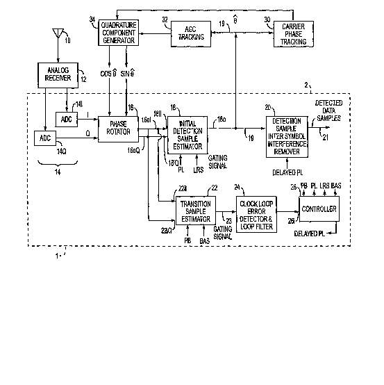
FIGURE 1 is a simplified block diagram of a
parallel pipeline hardware implementation or embodiment
of a receiver/demodulator according to an aspect of the
-9-
CA 02399714 2002-08-09
WO 01/59980 PCT/USO1/00690
invention including an initial detection sample
estimator, a transition sample estimator, and a
controller;
FIGURE 2 is a simplified block diagram of an
alternative configuration of a portion of the arrangement
of FIGURE 1;
FIGURE 3 illustrates a plot of signal amplitude
versus time during sequential symbol intervals sampled at
just under two samples per symbol;
FIGURE 4 is a simplified block diagram of the
initial detection sample estimator of FIGURE 1;
FIGURE 5 is a simplified block diagram of the
transition sample estimator of FIGURE 1;
FIGURE 6 is a simplified block diagram of the
controller of FIGURE 1; and
FIGURE 7 is a state diagram illustrating the
operation of a state machine portion of the controller of
FIGURE 6.
Description of the Invention
In FIGURE 1, an antenna 10 receives at least
one BPSK or QPSK modulated carrier, and couples it to an
analog receiver. The analog receiver may include such
processing as low-noise amplifiers, downconverters,
frequency selection filters, gain, and possibly other
processing such as, for example, gain control, all as
known in the art. The output signal produced by analog
receiver 12 is a pair (I and Q) of modulated analog
-10-
CA 02399714 2002-08-09
WO 01/59980 PCT/USO1/00690
carriers at baseband, where the modulation is at some
symbol rate. The baseband signals are applied to a set
14 of two analog-to-digital converters 14a and 14b of a
digitally implemented demodulator 2. Digitally
implemented demodulator 2 includes blocks 14a. 14b. 16,
18, 20, 22, 24, and 26. ADCs 14a and 14b sample the
baseband I and Q components, respectively, applied from
analog receiver 12 at a clock rate such that the samples
are in the range of 1 to 2 samples per symbol of the
received carrier. More specifically, the clock rate is
such that there is more than one sample per symbol and
less than two samples per symbol. The digital samples
are applied to a phase rotator block 16 together with the
estimated carrier phase . Phase rotator block 16 can be
implemented as a complex multiplier, and is used to
correct the phase of the I and Q samples, primarily for
the static phase error attributable to the transmission
path length, as well as for frequency offsets
attributable to oscillator frequency offsets between the
transmitter and receiver, and also, perhaps, for doppler
frequency shifts. Phase rotator block 16 is identical in
principle to the phase rotator described in PCT
application PCT/US97/16349 filed September 19, 1997 for
Thomas et al., and published March 26, 1998 as
WO_98/12849, and is generally well known.
The phase-corrected I and Q samples from phase
rotator 16 of FIGURE 1 are applied over signal paths l6oI
-11-
CA 02399714 2002-08-09
WO 01/59980 PCT/USO1/00690
and l6oQ, respectively, to input ports l8iI and l8iQ,
respectively, of initial detection sample estimator 18.
The following description of the initial detection sample
estimator assumes that carrier and clock synchronization
have been achieved by appropriate loops, but it should be
understood that the initial sample estimator will operate
during initial acquisition, producing "wrong" results,
which results.in turn tend to drive the loops to the
correct values. Initial detection sample estimator 18
receives Left-Right-Sample (LRS) gating signals and left
position (PL) variables. According to an aspect of the
invention, initial detection sample estimator 18 pairs
(generates two-sample sets of) sequential received
samples, weights the samples with weights dependent upon
the PL values, and sums the weighted sample pairs, to
produce an initial detection sample estimate for each
symbol, in the form of a signed multibit value. The sign
and the magnitude of the samples are significant because
the carrier and AGC errors are derived from the value.
The initial detection sample estimator 18 of FIGURE 1
differs from the corresponding sample estimator described
in the abovementioned Thomas et al. application, at least
in that it contemplates a field-programmable gate array
(FPGA) implementation. The field-programmable gate array
implementation is remotely reprogrammable, and thus does
not need the "case" variable described in the
abovementioned application to select among various sets
-12-
CA 02399714 2002-08-09
WO 01/59980 PCT/USO1/00690
of weights. The initial detection sample estimator 18 of
FIGURE 1 also differs from that of the abovementioned
application in that it includes additional multipliers
and a ROM which, taken together, allow a potential
estimate sample to be produced at each clock interval.
The initial estimates are applied from block 18 over a
path 19 to a detection sample intersymbol interference
removal circuit or block 20, which may be identical to
that described in the Thomas et al. application.
Intersymbol interference removal block 20 tends to remove
the most significant portions of intersymbol interference
attributable to the initial detection sample estimation
stage. Intersymbol interference removal block 20
produces I and Q "final" multibit soft decisions on a
signal path 21. The multibit soft decisions include a
sign bit representing the hard decision, and a complete
sign and magnitude value which can be used by later
stages of processing, such as forward error correction
decoders, to make better decisions about what was
transmitted.
The phase-corrected I and Q samples produced by
phase rotator 16 of FIGURE 1 at output ports l6oI and
l6oQ, respectively, are also applied to input ports 22iI
and 22iQ, respectively, of a transition sample estimator
22. Transition sample estimator 22 also receives before
position (PB) variables and Before-After-Symbol (BAS)
gating signals. In some cases, the PB weighting control
-13-
CA 02399714 2002-08-09
WO 01/59980 PCT/USO1/00690
signals may be equal to the PL weighting control signals,
Transition sample estimator 22 pairs sample pairs,
weights the samples with weights dependent upon the PB
values, and sums the weighted pairs to produce a
transition sample estimate for each symbol, in the form
of a signed multibit value. The sign and magnitude of
the samples is significant because the clock error is
derived from the value. From block 22, the transition
sample estimate is applied to a block 24, which
represents a clock loop error detector and loop filter,
which in effect differentiates the I and Q transition
samples, and sums the differentiated samples to produce
its output. The differentiation is controlled by the
values of the I and Q estimated hard decisions, as known
in the art, i.e. it is part of the general class of
decision directed loops. The clock loop error detector
and loop filter 24 of FIGURE 1 are identical in principle
to those of the abovementioned Thomas et al. application,
and axe well known in the art.
The output of clock loop error detector and
loop filter 24 of FIGURE 1 is applied to a controller
illustrated as a block 26. Block 26 generates gating
signals and P (sample timing position within the symbol
interval) weighting control values in response to the
estimated timing input from block 24. The controller can
be programmed to incorporate the actual value of P which
is required for the particular sample-per-symbol rate of
-14-
CA 02399714 2002-08-09
WO 01/59980 PCT/USO1/00690
the signals being processed. Consequently, a OP input to
the controller block is not required, as in the
arrangement of the Thomas et al. application. Of course,
some input path must be provided by which the
reprogramming can be accomplished, such as the
configuration inputs of an FPGA. The controller 26
receives the estimated timing input at its input port
26i, sums the estimated timing value with a free-running
P value to produce a corrected P value, which is then
delayed to produce the PB, PL, and delayed PL signals.
In addition, the corrected P value is applied to a state
machine which produces the LRS and BAS gating signals.
In FIGURE 1, the initial detection sample
estimates are applied over signal path 19 to a carrier
phase tracking block 30 and to an automatic gain control
(AGC) block 32. The carrier phase tracking block 30
processes the initial detection sample estimates as known
in the prior art to produce (theta hat), the estimated
carrier phase. The estimated carrier phase is applied to
a quadrature component generator block 34, which
generates sine and cosine components of the estimated
carrier phase. The AGC tracking circuit processes the
initial detection sample estimates, also by means known
in the art, to produce amplitude estimates, which could
be applied to the analog receiver in known fashion for
gain control, but which in this embodiment are applied to
-15-
CA 02399714 2002-08-09
WO 01/59980 PCT/USO1/00690
the quadrature component generator where the amplitude
estimates are used to scale the sine and cosine
components to effect a gain adjustment.
FIGURE 2 represents an alternative to the
analog receiver 12 of FIGURE 1 and ADCs 14I, 14Q. In
FIGURE 2, analog receiver 212 performs the same general
function as receiver 12 of FIGURE 1, but differs in that
the output signal is produced as a modulated carrier at
an intermediate frequency (IF), rather than as baseband I
and Q components. In the embodiment of FIGURE 2, a single
analog-to-digital converter (ADC) 214 converts the IF
signal to digital form. A further block 216 represents
generation of the I and Q digital components from the
digital IF signal. These I and Q digital components can
be applied directly to phase rotator 16 of FIGURE 1.
FIGURE 3 illustrates a plot 300 of signal
amplitude versus time during four sequential symbol
intervals T1-to-T2 (T1-T2), T2-T3, and T3-T4, denominated
as symbols 1, 2, 3, and 4. The plot 300 may be conceived
of as being applicable to both initial detection sampling
and transition estimate sampling. Times T1, T2, T3, T4,
and T5 represent the symbol transition times. The
sampling rate in FIGURE 3 is selected to be a trifle less
than two samples per symbol, so that most symbols have
two samples during their intervals, and only an
occasional symbol has a single sample. In interval T1-T2
(in symbol 1) of FIGURE 3, plot 300 takes on illustrative
-16-
CA 02399714 2002-08-09
WO 01/59980 PCT/USO1/00690
positive values, and is illustrated as being sampled at
times Ta and Tb. In symbol 2 interval T2-T3, the plot
takes on illustrative negative values, and sampling
occurs at times designated Tc and Td, and in symbol 3
interval T3-T4, the plot also includes negative values,
and sampling occurs at times Te and Tf. In symbol 5
interval T4-T5, the plot takes on positive values, and is
illustrated as being sampled at time Tg. Within symbol
interval T1-T2, the ideal detection time is TDlz, halfway
or midway between (in temporal space or time) symbol
transition times T1 and T2. Within symbol 2 interval T2-
T3, the detection time is designated TDz3, and in symbol
intervals T3-T4 and T4-T5, the detection times are
designated TD34 and TD45, respectively. It will be clear
that the sampling times Ta, Tb, Tc, Td, Te, and Tf do not
exactly correspond with the symbol transition times T1,
T2, T3, T4, and T5 , nor with the detection times TDlz,
TDz3, TD34 and TD45. For the case of detection sampling,
sampling time Ta in symbol 1 of FIGURE 3 lies to the left
of detection time TDlz, so is designated as a "left" (L)
sample. Similarly, sampling time Tc in symbol 2 lies to
the left of detection time TDz3, so is designated "L." In
symbol 3, sample time Te is also designated L. Also in
symbol 1, the sample occurring at time Tb lies to the
right of detection time TD12, so is designated "R."
Sample Td in symbol 2, Tf in symbol 3, and Tg in symbol 4
are also designated R. Note that sample Tf is used both
-17-
CA 02399714 2002-08-09
WO 01/59980 PCT/USO1/00690
as a Right sample for symbol 3 and as a Left sample for
symbol 4. In general, it is possible for a sample to be
both B and A or L and R.
For the case of transition sampling, sampling
time Tb in symbol 1 of FIGURE 3 lies to the left of
transition time T2, so is designated as a "before" (B)
sample. Similarly, sampling time Tc in symbol 2 lies to
the right of, or after, transition time T2, so is
designated "A." In symbol 2, sample Td occurs before its
associated transition time T3, so is labelled as "B."
In symbol 3, sample time Te is after the transition time
T3, so is designated A, and sample time Tf is B.
Finally, by the same token as the Left and Right samples
above, Tg is used as an After sample (for the symbol 3-4
transition) and as a Before sample (for the symbol 4-5
transition).
FIGURE 4 is a simplified block diagram of
initial detection sample estimator 18 of FIGURE 1. In
FIGURE 4, the I digital samples from phase rotator 16
output port l6oI are applied to a delay block 410, to
compensate for delays in the derivation of the P values
for the lookup tables, as is conventional. The Q digital
samples from phase rotator 16 output port l6oQ are
applied to a delay block 430. The delayed I signals
produced at the output of delay block 410 are applied
over a path 411 to a further delay block 412 and to a
multiplier (X) block 414. Multiplier 414 receives the
-18-
CA 02399714 2002-08-09
WO 01/59980 PCT/USO1/00690
signals from path 411 and multiplies the signals by
"right" weights 1-wL from a read-only memory 416, which
produces the weights under the control of PL address
signals. The weights are determined by the linear
combination of left and right samples which maximizes the
signal-to-noise ratio.(SNR) as given by
W L S~-L) '~' W r S~~"
The output signals of multipliers 414 and 418 are
temporary signals
tl-IkG*WkG
where W is the coefficient, IkL and IkR are the left and
right detection path samples, respectively. Formulas for
determination of weights W can be found in S. Sayegh,
"DSP MCD for Future IBS/IDR Services," Second
International Workshop on Digital Signal Processing
Techniques Applied to Space Communications, 1990. It
should be understood that in the context of a field-
programmable gate array, the values stored in the various
memory addresses of ROM 416 and other ROMs can be
reprogrammed in an appropriate manner for any particular
value of samples per symbol or alternative method of
determining weights. The actual value of weight 1-wL
produced at the output of ROM 416 is determined from
sample to sample by the address PL signal applied to the
ROM at the sample instant. The weight produced by ROM
-19-
CA 02399714 2002-08-09
WO 01/59980 PCT/USO1/00690
416 is given by where h(*) is the impulse response of
the raised cosine filter.
_ lz(R) - h(L) lz(L + R)
~1- lz(L - R)~(lz(L) + lz(R))
Referring to FIGURE 3, the current sample
exiting delay 410 of FIGURE 4 may be considered to be the
sample at time Tb of FIGURE 3, in which case the sample
exiting delay 412 of FIGURE 4 must be an earlier sample,
or the sample of time Ta of FIGURE 3. Thus, the sample
leaving delay 412 is designated as "early" and the sample
leaving delay 410 is designated "late." Multiplier 414
multiplies the late signal received over signal path 411
by weight 1-wL. The output value of the weighting signal
1-wL produced by ROM 416 depends upon the predetermined
values stored in the various memory locations and on the
address (PL) at the time of the signal sample.
Multiplier 414 thus produces a product signal which is
the product of a weight multiplied by a late sample.
In FIGURE 4, the delayed I signal at the output
of delay block 412 is applied to a further multiplier (X)
418. Multiplier 418 also receives a weighting signal w
from a ROM 420, under the control of PL signals. The
left weighting signal is given by
_ h(L) - h(R) h(L - R)
W L ~1- h(L, + R)J(h(L) + lz(R)~
-20-
CA 02399714 2002-08-09
WO 01/59980 PCT/USO1/00690
As mentioned, delay 412 produces an "early" signal
(relative to the signal at the output of delay block
410). Multiplier 418 multiplies the early sample from
delay block 412 by the "left" weighting signal wL, and
produces a temporary product signal which may be
denominated "LE."
tz=Ixn*(1-Wxz,~
The LE and RL signals from multipliers 414 and 418 are
applied to a summing circuit 422, which produces the sum
of the. two product signals, namely LE+RL.
As illustrated in FIGURE 3, there are about two
samples per symbol, but the pairs of samples at Ta, Tb;
Tc, ,Td; Te, Tf drift relative to the underlying symbol
timing, because the number of samples per symbol is not
exactly two. Consequently, in symbol 4 occupying time
T4-T5, there is only one sample, namely the one at time
Tg. Depending upon the exact complex-sample-per-symbol
ratio in the range between greater-than-one and less-
than-two, most of the symbols may contain (or be
associated with) two samples, as illustrated in FIGURE 3,
or most of the symbols may have only one sample, with an
occasional symbol having (being associated with) two
samples.
The samples at the output of summing circuit
422 of FIGURE 4 may be considered to be "provisional"
estimates of the detection sample estimator. However,
-21-
CA 02399714 2002-08-09
WO 01/59980 PCT/USO1/00690
since the symbol can have only one value, it cannot be
represented by two estimates. Instead, only one sample
is gated through gate 424 to signal path 426 for each
symbol interval. When a symbol interval includes two
samples, that one of the two samples which most closely
represents the "true" value of the detection estimate is
chosen.
There are alternative ways to compute the
weighting coefficients. For example, extensive
simulation has shown that simple linear weighting
produces results almost as good as the theoretically
optimal weighting of equations 3 and 4. In such a linear
weighting scheme, the weight is established by the
distance of the sample from the detection (or transition)
point normalized by OP, such that
Left Weight = (OP-d)/OP; and
Right Weight = 1 - wL
where "d" is the distance of the sample from the point
being estimated and a symbol interval is represented by
"1" (that is, normalized). In. this example, OP=1/(#
complex samples per symbol).
The sum signal LE+RL produced by summing
circuit 422 of FIGURE 4 may be viewed as the sum of
weighted pairs of samples. As described below, the
weighting is determined as a function of how close the
sample is to the detection instant. Thus, if a sample
_22_
CA 02399714 2002-08-09
WO 01/59980 PCT/USO1/00690
happens to occur exactly at the detection instant, half-
way between the transition times of FIGURE 3, it is given
a weight of unity or 1. As the sample approaches ~P away
from the detection point, the weight decreases
progressively, reaching a value of zero or 0 at the end
point. Analysis has revealed that, when two samples
occur during a symbol interval, the later-occurring of
the provisional estimates of the sample is always the
better choice for gating to the output port 4240 of the
gate 424. The gating of gate 424 is controlled by a
left-right-sample (LRS) gating signal applied from a path
425.
The Q signal from output port l6oQ of phase
rotator 16 of FIGURE 1 is applied to delay block 430 of
initial detection sample estimator 18 of FIGURE 4. In
general, delay 430 may be deemed to be equivalent of
delay 410, and of practical importance, but not important
to a theoretical understanding of the invention. The
delayed signal produced by delay 430 may be deemed a
"late" signal, which is applied to a further one-sample
delay 432 to produce an "early" signal. Multiplier 434
multiplies the R weight from ROM 416 by the late signal
to produce a RL product signal, and multiplier 438
multiplies the L weight by the early signal to produce a
product LE signal. The RL and LE signals representing Q
components are applied from multipliers 434 and 438 to a
-23-
CA 02399714 2002-08-09
WO 01/59980 PCT/USO1/00690
summing circuit 444, which sums the product signals to
produce sum signal RL+LE. The RL+LE Q signal is gated to
an output port 4460 of a gate 446 in the same manner as
that described for gate 424, under the control of the
same LRS gating signal. The gated output signal on
signal path 446 represents the initial detection sample
estimate for Q.
FIGURE 5 illustrates~details of transition
sample estimator 22 of FIGURE 1. In general, the
arrangement of FIGURE 5 operates much like the
arrangement of FIGURE 4, with the differences lying in
the timing and weight values. For the transition path,
analysis has shown that a simple linear weighting scheme,
similar to the alternative scheme described above for the
detection path, is entirely satisfactory. In order to
make this correspondence between the arrangement of
FIGURE 5 and that of FIGURE 4 more clear, elements of
FIGURE 5 substantially corresponding to those of FIGURE 4
are designated by like reference numerals in the 500
series rather than in the 400 series. In FIGURE 5, the
phase corrected I signal is applied by way of input port
22iI to a synchronisation delay block 510, which is not
of interest in understanding the invention, and the phase
corrected Q signal is applied to a corresponding delay
530. The output of delay 510 on path 511 is the late
transition sample. The delayed sample on path 511 is
further delayed by a delay 512 to produce the early
-24-
CA 02399714 2002-08-09
WO 01/59980 PCT/USO1/00690
transition sample. The late and early transition samples
are applied to multipliers 514 and 516, respectively, for
multiplication by weights (1-aB) and aB, respectively.
The 1-aB weight is the weight applied to the late or
"after" sample, and is generated by ROM 516 in response
to PB address signals applied to its address input ports.
The 1-aB weight is multiplied by the late or after
sample to produce an AL signal at the output of
multiplier 514. The aB weight is read from ROM 520 under
the control of PB address signals, and is multiplied by
the early or "before" sample in multiplier 518, to
produce a BE sample. The AL sample from multiplier 514
and the BE sample from multiplier 518 are applied to the
input ports of a summing circuit 522 Summing circuit 522
sums the two I product signals to produce a provisional I
transition sample estimate which is the sum of products.
In the Q channel of the arrangement of FIGURE
5, the phase corrected Q sample signals are applied to
input port 22iQ of a delay 530, which needs no
discussion, to produce a late sample, and the Q signal is
further delayed by a delay 532 to produce an early
sample. A multiplier 534 multiplies the late Q sample by
the 1-aB weight from ROM 516, to produce an AL Q product
sample, and a multiplier 538 multiplies the early Q
sample by the aB weight, to produce a BE Q product
sample. Both the AL and the BE Q sample signals are
applied to a summing circuit 544 to produce a sum of the
-25-
CA 02399714 2002-08-09
WO 01/59980 PCT/USO1/00690
Q product signals, which is a provisional Q transition
sample estimate.
The provisional I product sample signals
produced by summing circuit 522 of FIGURE 5 are applied
to a gate 524. The provisional Q product sample signals
produced by summing circuit 544 are applied to a gate
546. Gates 524 and 546 respond to Before-After-Sample
(BAS) gating signals applied over a signal path 525, to
gate to their output ports 524o and 5460, respectively,
only one sample during each symbol interval. When only
one sample occurs during a given symbol interval, it is
gated to the output port of the gate, to become the I or
Q transition sample estimate. When two samples occur
within a symbol interval, only one is gated to the output
port of the gate. Analysis has shown that the proper
estimate of the transition sample is always the earlier
of the two samples occurring in that symbol interval
having two provisional samples. Thus, gates 524 and 546
gate to their output ports 524o and 5460, respec ively,
only the earlier of two provisional transition sample
estimates, under the control of the BAS gating signal.
The I and Q transition sample estimates are coupled onto
signal path 23 for application to clock loop error
detector and loop filter 24 of FIGURE 1.
FIGURE 6 is a simplified block diagram of
controller 26 of FIGURE 1. In FIGURE 6, the estimated
timing signal from clock loop error detector and loop
-26-
CA 02399714 2002-08-09
WO 01/59980 PCT/USO1/00690
filter 24 of FIGURE 1 is applied by way of input port 26i
to a first input port of a summing circuit 610. Summing
circuit 610 also receives a free-running position (P)
signal from a generator 612. The P signal, it will be
recalled, is the sample time "position" within a symbol
interval. Generator 612 is a synchronous counter which
increments by OP at the clock instant for each cycle,
where OP is the change in sample time from one sample to
the next expressed in terms of a symbol time, as
described above. Thus, the value of ~P must be known a
priori.
Generator 612 of FIGURE 6 is a modulo counter,
in that it "rolls over" at some maximum count determined
by the size of a register 614. In a particular
embodiment of the invention, register 614 has 14 bits,
corresponding to 16,384 states; it thus rolls over at
numerical count 16383. A symbol is deemed to occur
during the count of 0 to 16,383, and the detection point
is deemed to be the center count, namely 8192. The
output of register 614 is applied to the input of a
summing circuit 616, which adds to the current register
count the value of QP. The value of OP may be internally
stored in a programmable FPGA implementation of the
structure, or it may be supplied from an external source
in the case of nonprogrammable embodiments. The value of
14 bits was found by experiment to be optimal in this
-27-
CA 02399714 2002-08-09
WO 01/59980 PCT/USO1/00690
particular embodiment.
In the arrangement of FIGURE 6, the free-
running P value produced by generator 612 is corrected by
summing with the estimated timing signal from input port
26i in summing circuit 610. Thus, the output from
summing circuit 610 is the timing-corrected P value. The
timing-corrected P value from summing circuit 610 of
FIGURE 6 is applied to a one-sample-clock delay 618. The
one-sample-delayed corrected P value is applied to
further one-sample delay 620 and to a clock gate state
machine designated as 622. The output of delay 620
represents the PB and PL weighting control signals. The
PB signals are routed to transition sample estimator 22
of FIGURE 1, and the PL signal is routed to initial
detection sample estimator 18 of FIGURE 1. The output of
delay block 620 is also applied to a gated delay block
624, which gates the signal to output port 6240 in
response to the LRS gate signal. The gated signal from
output port 624o is applied to a further gated delay 626,
which gates its input signal to its output signal path
628 in response to the same LRS gate signal, to produce
the delayed PL signal, which is applied to detection
sample intersymbol interference remover 20 of FIGURE 1.
Clock gate state machine 622 of FIGURE 6
receives the one-sample delayed corrected position (P)
value from delay 618, and also receives the ~P signal,
_28-
CA 02399714 2002-08-09
WO 01/59980 PCT/USO1/00690
either from generator 612, or from an internally stored
value. Programming input paths 62213, illustrated in
phantom, may be used to program the state machine if the
~P values are not internally stored. State machine 622
includes two portions, a detection state portion
designated 710 and a transition state portion 750 in
FIGURE 7, and steps through the states set forth in
FIGURE 7, to generate the gating signals necessary to
select the appropriate samples at each stage of
processing of the system of FIGURE 1. The state machine
specifications are given in pseudocode as:
Detection Path
State DL;
SampGate=1;
{Samples are always enabled for less than 2 s/s}
SymGate=1;
if TestD gotoDRL else goto DR;
{which is required for s/s > 1.5}
State DRL
SampGate=1;
SymGate=1;
if TestD goto DRL else goto DR
{required for s/s < 1.5}
-29-
CA 02399714 2002-08-09
WO 01/59980 PCT/USO1/00690
State AR
SampGate=1;
SymGate=0;
goto DL;
Transition Path
State TB
BAS gate =1
if TestT goto TAB else goto TA
State TAB
BAS gate = 1
if TestT goto TAB else goto TA
State TA
BAS gate = 0
goto TB
where:
TestD = <is True when> (NextP >_ (24576 - OP)) OR
(NextP < (~P - 8192)); and
NextP = PO + ~P
TestT = <is True when> (NextP>=(16384 - OP)) AND
(NextP < OP); and
-30-
CA 02399714 2002-08-09
WO 01/59980 PCT/USO1/00690
NextP = PO + OP
These states and state transitions are illustrated in
FIGURE 7, in which 712 represents the DL state, and 714
represents the "if TestD = True" path to the DRL state
716. Path 718 represents the state transition from state
DL to state DR if TestD is False. State DR is designated
724. The SymGate = 1 in both the DL and DRL states,
State transition 720 represents the path from state DRL
back to itself if TestD is True, and state transition 722
represents the trajectory if TestD is False. State DR
always transitions to state DL by way of transition 726.
In state DL, the SymGate = 0. Similarly, state
TB of FIGURE 7 is represented by 752, and state
transition 754 represents a transition to state TAB if
TestT is true. State TAB is designated 756. The BAS
gate = 1 in both states TB and TAB. The transition from
state TB if TestT is false is designated as 758, and
leads to state TA, designated as 724. State transition
770 represents remaining in the TAB state, by means of
path 770, if TestT = True, and state transition 772 leads
to state TA if TestT = False. The BAS gate = 0 when in
state TA. State TA always transitions to state TB by way
of state transition 776. The state machines may be
implemented by any number of well-known methods,
including state maohine compilers, lookup table
-31-
CA 02399714 2002-08-09
WO 01/59980 PCT/USO1/00690
implementations, and custom designs.
The demodulator according the invention is
particularly useful for spacecraft applications, where
extremely high sample rates are required in order to
sample multicarrier analog signals, and also in handheld
communications receivers, where extremely low operating
power is an important parameter.
Other embodiments of the invention will be
apparent to those skilled in the art. For example, the
entire method as described herein could be programmed
into a DSP microcomputer using a single multiplier
sequentially to perform the weighting function, and other
equivalent features of the DSP circuit, such as memories,
for lookup table storage, or direct computation of
weighting factors as required, for a low-speed
implementation.
Thus, a demodulator (2) according to an aspect
of the invention is for demodulating an analog signal
representing a series of digital symbols. The analog
signal may represent a series of digital bits in a phase-
shift-keyed signal or in a quaternary-shift-keyed signal.
The demodulator (2) includes an analog-to-digital
converter (14) for converting the analog signal into
digital form at a sample rate lying in the range between
1 and 2 complex samples per symbol, noninclusive, to
thereby produce a stream of data samples. In this
context, the word "noninclusive" means that the sample
-32-
CA 02399714 2002-08-09
WO 01/59980 PCT/USO1/00690
rate does not include the end values of the range, which
is to say that the sample rate does not include 1 or 2
complex samples per symbol. The demodulator (2) also
includes a digitally implemented demodulator (16, 18, 20,
22, 24, 26) coupled to the analog-to-digital converter
(14), for demodulating the stream of data samples. The
digitally implemented demodulator (16, 18, 20, 22, 24,
26) includes (a) an initial detection sample estimator
(18) for examining temporally adjacent pairs (the sample
pairs at times Ta, Tb; Tb, Tc; Tc, Td, for example) of
the stream of data samples, and for generating a
provisional initial detection sample (at port 4220) for
each temporally adjacent pair of the samples. As a
result of this pairing and the sample rate lying between
l and 2 complex samples per symbol, some symbol intervals
produce one such provisional initial detection sample,
and some symbol intervals produce two such provisional
initial detection samples. The digitally implemented
demodulator (16, 18, 20, 22, 24, 26) also includes (b) a
gating arrangement (424, 444) for gating only one
provisional initial detection sample for each symbol, and
the gating arrangement (424; 424, 444) gates only the
second such provisional initial detection sample
occurring within symbols producing two such provisional
initial detection samples. The resulting gated samples
(at output ports 4240, 4460) are components (I and/or Q)
of the initial detection samples. The digitally
a
-33-
CA 02399714 2002-08-09
WO 01/59980 PCT/USO1/00690
implemented demodulator (16, 18, 20, 22, 24, 26) also
includes (c) an intersymbol interference remover (20)
coupled to the gating arrangement (424, 446) of the
digitally implemented demodulator (16, 18, 20, 22, 24,
26), for removing at least some intersymbol interference
from those provisional initial detection samples gated by
the gating arrangement (424; 424, 446).
In one version, the digitally implemented
demodulator (16, 18, 20, 22, 24, 26) further includes a
transition sample estimator (22) for examining temporally
adjacent pairs of the stream of data samples, and for
generating provisional transition samples (on path 23)
for each temporally adjacent pair of samples. Under
these circumstances, some symbol intervals produce one
such provisional transition sample, and some symbol
intervals produce two such provisional transition
samples. This version also includes a gating arrangement
(524, 526) for gating only one (complex) provisional
transition sample for each symbol, and the gating
arrangement (524; 524, 546) gates only the first-
occurring such provisional transition sample occurring
within symbols producing two such provisional transition
samples, so that the gated samples are transition
samples.
In another view, a digitally implemented
demodulator (16, 18, 20, 22, 24, 26) is for demodulating
a stream of data samples representing a phase-shift-keyed
-34-
CA 02399714 2002-08-09
WO 01/59980 PCT/USO1/00690
data stream sampled at less than two and greater than one
complex samples per symbol, which stream of samples has a
particular sample-per-symbol rate during any given
transmission. The sample-per-symbol rate may vary from
time to time. The digitally implemented demodulator (16,
18, 20, 22, 24, 26) generates an output digital data
stream, and includes an initial detection sample
estimator (18) coupled to receive the stream of data
samples sampled at less than two and more than one
complex samples per symbol. The initial detection sample
estimator (18) includes (a) a first multiplier (414)
coupled to receive the stream of data samples and right
weighting coefficients (from ROM 416), for multiplying
the right weighting coefficients by the stream of data
samples, for thereby producing late product signals, (b)
a first sample delay (412) for delaying the stream of
data samples by one sample interval to produce early
detection samples, (c) a second multiplier (418) coupled
to the first sample delay (412) for multiplying the early
detection samples by left weighting coefficients (from
ROM 420) to thereby produce early detection product
signals; (d) a summing arrangement (422) coupled to the
first (414) and second (418) multipliers, for summing the
early and late product signals for producing summed
detection product signals, and (e) a detection gating
arrangement (424) coupled to the summing arrangement,
where the detection gating arrangement includes an output
-35-
CA 02399714 2002-08-09
WO 01/59980 PCT/USO1/00690
port (4240) and a gating signal port, for gating to the
output port (4240) of the detection gating arrangement
(424) those of the summed detection product signals
identified by detection gating signals (LRS), and for not
gating to the output port (4240) of the detection gating
arrangement (424) those of the summed product signals not
identified by the detection gating signals (LRS), for
thereby generating (on path 19) initial detection
estimates. The digitally implemented demodulator (16,
18, 20, 22, 24, 26) also includes a detection sample
intersymbol interference remover (20) coupled to the
output port (180) of the detection gating arrangement
(18), for removing from the initial detection estimates
that intersymbol interference attributable to the actual
sample times, relative to the symbol interval, used to
produce the initial detection estimates, to thereby
produce soft detection output signals including
provisional hard decision (sign) information. The
digitally implemented demodulator (16, 18, 20, 22, 24,
26) further includes a transition sample estimator (22)
coupled to receive the stream of data samples. The
transition sample estimator (22) includes (a) a third
(514) multiplier coupled to receive the stream of data
samples together with after weighting coefficients (from
ROM 516), for multiplying the after weighting
coefficients by the stream of data samples, for producing
late product signals, (b) a second sample delay (512) for
-36-
CA 02399714 2002-08-09
WO 01/59980 PCT/USO1/00690
delaying the stream of data samples by one sample
interval to produce early samples, (c) a fourth
multiplier (518) coupled to the second sample delay (512)
for multiplying the early transition samples by a before
weighting coefficient to thereby produce early product
signals; (d) a second summing arrangement (522) coupled
to the third (514) and fourth (518) multipliers, for
summing the early and late product signals for producing
summed product signals, and (e) a transition gating
arrangement (524) coupled to the second summing
arrangement (522). The transition gating arrangement
(524) includes an output port (5240) and a gating signal
port, for gating to the output port (5240) of the
transition gating arrangement (524) those of the summed
product signals identified by transition gating signals
(BAS), and for not gating to the output port (5240) of
the transition gating arrangement (524) those of the
summed product signals not identified by the transition
gating signals (BAS). The gated summed transition
product signals are the transition estimates. Lastly,
the digitally implemented demodulator (16, 18, 20, 22,
24, 26) includes a control arrangement (26) coupled to
the detection (424; 424, 446) and transition (534; 534,
546) gating arrangements, for generating the detection
(LRS) and transition (BAS) gating signals. The detection
gating signals (LRS) are generated in a manner such as to
identify for gating to the output port of the detection
-37-
CA 02399714 2002-08-09
WO 01/59980 PCT/USO1/00690
gating arrangement only one provisional detection
estimate during each symbol interval, and in a manner
such as to identify for gating to the output port of the
detection gating arrangement the later-occurring of the
two provisional detection estimates occurring during
those symbol intervals in which two provisional detection
estimates are generated, The control arrangement
generates the transition gating signals (BAS) in a manner
such as to identify for gating to the output port of the
transition gating arrangement only one provisional
transition estimate during each symbol interval, and so
as to identify for gating to the output port of the
transition gating arrangement the earlier-occurring of
the two provisional transition estimates occurring during
those symbol intervals in which two provisional
transition estimates are generated.
A method according to an aspect of the
invention is for generating initial estimates of
detection samples. The method comprises the steps of
providing left and right weighting signals (from ROMS 416
and 420), and sampling (ADC 14I; 14I, 14Q) a stream of
data at less than two and greater than one complex.
samples per symbol. As a result of this sampling rate,
or whereby, at least some symbol intervals include two
samples. The stream of data sampled at less than two and
greater than one complex samples per symbol is multiplied
(414) by the right weighting signals to produce late
-38-
CA 02399714 2002-08-09
WO 01/59980 PCT/USO1/00690
product signals. The stream of data is delayed (412) by
one sample interval to thereby produce early signals.
The early signals are multiplied (418) by the left
weighting signals to produce early product signals. The
early and late product signals are summed (422) to
produce summed signals. The summed signals are gated
(26, 424) so as to pass only one summed signal per symbol
interval. In a particular mode of this method, the step
of gating passes only the second-occurring one of the
summed signals in a symbol when two summed signal samples
occur during a symbol interval. Ideally, the left and
right weighting signals are dependent upon the sampling
time within a symbol interval.
-39-