Note: Descriptions are shown in the official language in which they were submitted.
CA 02400492 2002-08-23
WO 01/63777 PCT/USO1/05654
INTERFERENCE CANCELLER
FIELD OF THE INVENTION
The present invention relates to the field of electromagnetic energy
interference cancellation.
BACKGROUND OF THE INVENTION
Receivers, for example radio frequency ("RF") receivers, are typically
designed to operate in a given bandwidth (e.g., UHF or microwave bands) and
may
also be designed to operate over multiple bandwidths. Receivers may be
designed to
operate on signals occupying a subset of the receiver's overall operating
bandwidth.
Such a subset may be called a "channel." The frequency at the center of a
channel's
bandwidth may be called the "channel frequency." Electromagnetic signals from,
for
example, RF transmitters, may interfere with a receiver's operation even if
the
electromagnetic signals' frequency spectra do not substantially overlap the
receiver's
channel frequency. Out-of channel (also known as out-of band) interference
signals
can create adverse effects in a receiver (e.g., desensitization, cross-
modulation, and
intermodulation). In environments such as airports, communications facilities,
or
mobile platforms, interference signals are of particular concern due to the
proximity
of co-located transmitters and receivers. It is desirable to suppress out-of
channel
interference signals incident on a receiver's input.
Tunable, or even fixed, preselector filters placed in series with and
preceding
a receiver may offer some suppression of out-of channel signals (and therefore
some
reduction in adverse effects), however, such filters are typically costly.
Preselector
filters typically possess bandwidths that are substantially larger than the
operating
channel bandwidth, which is especially true for tunable preselector filters.
Furthermore, such filters add weight and occupy physical space that may not be
available in certain platforms. Additionally, preselector filters can
introduce
distortion by, for example, preselector filter group delay.
Devices known as cosite interference cancellers, typically used in
environments having co-located transmitters and receivers, have been used to
reduce
the amount of interference signal that is incident on a receiver. However,
known
applications of cosite interference cancellers require that a reference
signal, sampled
CA 02400492 2002-08-23
WO 01/63777 PCT/USO1/05654
from a source external to the cosite interference canceller itself, be applied
to the
cosite interference canceller's circuitry. The reference signal is typically a
sample of
an interfering signal. This sample is subtracted from a composite signal; the
composite signal contains both the desired and interference signals. U.5.
Patent
Number 5,630,223 to Bahu et al. requires a plurality of filter circuits for
receiving
filtered transmission signals (i.e., samples of interference signals from
transmitters).
U.5. Patent Number 5,428,831 to Monzello et al. discloses a reference coupler
for
sampling the transmitted signal of a co-located radio transmitter. These
patents
exemplify a class of devices that require a hardwired connection of a
reference signal
(i.e., the interfering source of electromagnetic energy) to the cosite
interference
canceller. U.5. Patent Number 4,893,350 to Minamisono et al. discloses a
cosite
interference canceller that may be operated with interference sources that are
not
hardwired to the cosite interference canceller. Minamisono et al. discloses an
auxiliary antenna positioned in the direction of the interference signal for
collection
of essentially only the interference signal. The output of the auxiliary
antenna
supplies the interference canceller with a reference signal used to cancel the
interference signal from a composite signal collected by a main antenna.
Minamisono et al. is representative of a class of cosite interference
cancellers that use
auxiliary antennas to collect reference signals.
SUMMARY OF THE INVENTION
The present invention relates to a method and apparatus for interference
cancellation, where interference signals are derived from a composite signal,
and
where the composite signal contains both the desired and interference signals.
The
derived interference signal may be used as a reference signal for the
interference
canceller. A preferred embodiment does not require hardwiring or cooperation
between it and an interfering electromagnetic energy source. It operates on a
composite signal and may utilize a single input port for signal reception
(i.e., a
separate reference port is not required). No a priori knowledge of the
interfering
source's frequency spectrum is required.
The preferred embodiment derives its own reference signal by suppressing
the desired signal in a duplicate of the composite signal. Suppression of the
desired
signal is accomplished in a subcircuit of an interference canceller referred
to
2
CA 02400492 2002-08-23
WO 01/63777 PCT/USO1/05654
hereinafter as a Reference Circuit. The Reference Circuit derives a likeness
of the
interference signal. The likeness of the interference signal may be processed
so that
it is substantially equal in amplitude and opposite in phase to its
counterpart in the
original composite signal. The composite signal and likeness of the
interference
signal may be summed, thereby substantially canceling the interfering signal
from
the composite signal. The resultant signal, having a substantially suppressed
interference signal, may be applied to the input of a receiver. The Reference
Circuit
may be tunable.
The interference signal may be located close in frequency to the desired
signal. The desired signal may have weaker signal strength than the
interference
signal. No knowledge of the interference signal is needed preferably, only
knowledge of the desired signal's center frequency is required. The preferred
embodiment is useful to avoid desensitization of receivers through suppression
of
narrowband or wideband out-of channel interference. The method and apparatus
disclosed herein can be used in conjunction with various weight control
algorithms
(e.g., the Least Mean Square algorithm).
One object of the invention is to provide an improved interference canceller.
Another object of the invention is to provide an interference canceller that
does not need a priori knowledge of an interfering signal's electromagnetic
spectral
content.
Another object of the invention is to provide weak signal extraction by
suppression of strong interference signals.
Another object of the invention is to provide a reference circuit to suppress
desired spectral components from a composite signal containing both the
desired and
the interference spectral components, thereby leaving substantially only the
interference spectral components.
BRIEF DESCRIPTION OF THE FIGURES
Preferred embodiments of the present invention are hereinafter described with
reference to the accompanying drawings.
FIG. 1 illustrates a block diagram of a preferred embodiment of an
interference canceller.
CA 02400492 2002-08-23
WO 01/63777 PCT/USO1/05654
FIG. 2 illustrates a block diagram of a first embodiment of a reference
circuit
of the preferred embodiment of FIG. 1.
FIG. 3 illustrates a block diagram of an alternate embodiment of a reference
circuit of the preferred embodiment of FIG. 1.
FIG. 4 illustrates a more detailed block diagram of the first embodiment of
the reference circuit of FIG. 2.
DETAILED DESCRIPTION OF PREFERRED EMBODIMENTS OF THE
INVENTION
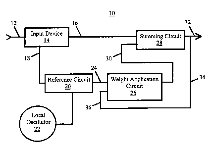
FIG. 1 illustrates a block diagram of a preferred embodiment of an
interference canceller 10. The interference canceller 10 generally operates as
follows. An input composite signal is applied to a first port 12 of an input
device 14.
The input composite signal contains both desired and interference signals. As
used
herein, the term "signal" refers to electromagnetic energy that may or may not
contain information. The input device 14 divides, splits or otherwise shares a
first
and second quantum of the composite signal between a first path 16 and a
second
path 18. A Reference Circuit 20 is operatively connected to the second path 18
and
receives its input therefrom.
The Reference Circuit 20 suppresses the desired signal included within the
second quantum of composite signal that was applied to the Reference Circuit
20.
The output of the Reference Circuit 20 includes predominantly a likeness of
the
interference signal. (For the purpose of description here, a "likeness" refers
broadly
to a correlated signal produced by any method, including but not limited to
operating
on energy taken from an original signal, generating a duplicate signal, or
otherwise,
and without limitation to ancillary signal processing, such as filtering,
amplifying,
etc. A likeness may also include the original signal itself.)
Suppression of the desired signal within the Reference Circuit 20 is
accomplished at an intermediate frequency, which is generally a frequency
other than
the desired signal's channel frequency. To convert the desired signal's
channel
frequency to the Reference Circuit's intermediate frequency, a local
oscillator (in
conjunction with other circuitry explained with reference to FIGS. 2, 3, and
4) is
used. The local oscillator 22 frequency preferably equals the center frequency
of the
desired signal plus or minus an intermediate frequency of the Reference
Circuit 20.
4
CA 02400492 2002-08-23
WO 01/63777 PCT/USO1/05654
The addition or subtraction of the intermediate frequency is dependent upon
whether
the Reference Circuit 20 first up-converts or first down-converts the input
composite
signal. The local oscillator 22 output is operatively connected to the
Reference
Circuit 20. The local oscillator 20 may be tunable.
The output of the Reference Circuit 20 is applied to a first input 24 of a
Weight Application Circuit 26. In the preferred embodiment, the Weight
Application
Circuit 26 is an analog-based Least Mean Square ("LMS") algorithm. Other
implementations may be possible, including, for example, a Recursive Least
Square
algorithm. Weight application algorithms may also be called adaption
algorithms
and have application in the field of adaptive filtering.
The Weight Application Circuit 26 adjusts, in a time-continuous fashion, the
amplitude and phase of the signal output by the Reference Circuit 20. The
amplitude
and phase adjusted signal is summed with the composite signal that was output
from
the input device 14 and was passed along the first path 16. Summing occurs in
a
summing circuit 28. The amplitude and phase adjusted likeness of the
interference
signal substantially cancels the interference signal present in the first
path's 16
composite signal. The output 32 of the interference canceller includes the
desired
signal and a substantially suppressed interference signal.
The Weight Application Circuit's 26 amplitude and phase adjustment is
enabled by a continuous sample of the signal from the output 32 of the
Interference
Canceller 10. The continuously sampled signal flows along a path 34 from the
canceller's output 32 to a second input 36 of the Weight Application Circuit
26. The
degree to which the interference signal remains at the canceller's output 32
is
dependent on the design of the Weight Application Circuit 26, designs of which
are
well known in the art.
FIG. 2 illustrates a block diagram of a first embodiment of a Reference
Circuit 20 of the preferred embodiment of FIG. 1. The composite signal input
from
the second path 18 (FIG. 1) of the input device 14 (FIG. 1) is applied to a
first port 38
of a first frequency converter 40. The first frequency converter 40 may be
used to
either up- or down-convert the composite signal to an intermediate frequency.
Choice of intermediate frequency may depend on, but is not limited to, such
aspects
as availability of circuit components, size limitations, and other circuit
design and
5
CA 02400492 2002-08-23
WO 01/63777 PCT/USO1/05654
manufacture considerations. The intermediate frequency may preferably be the
center frequency of an IF bandpass filter 42.
A second port 44 of the first frequency converter 40 is connected to a first
port 46 of a directional coupler 48. The directional coupler 48 allows signal
to flow
from the first port 46 of the directional coupler 48 to a second port 50 of
the
directional coupler 48 with modest insertion loss. The directional coupler 48
is
designed to attenuate the signal flowing from the first port 46 to a third
port 52 of the
directional coupler 48. The directional coupler 48 is designed to allow signal
to
flow, with some nominal attenuation, from the second port 50 to the third port
52.
The signal flowing from the second port 50 to the third port 52 is referred to
as the
"coupled" signal. In the embodiment of Fig. 2, the coupled signal is a reduced
amplitude copy, minus the desired signal, of the signal flowing from the
second port
50 to the first port 46. Other devices, having similar signal flow
directionality
features may be used, such as a circulator.
A bandpass filter 42 is operatively connected to the second port 50 of the
directional coupler 48. The bandpass filter 42 has a center frequency that is
preferably approximately equal to the intermediate frequency of the Reference
Circuit 20 (i.e., the center frequency of the desired signal offset by the
local oscillator
22 frequency of the first frequency converter 40). The passband of the
bandpass
filter 42 is preferably wide enough to allow the desired signal to pass
through the
bandpass filter 42 and into a termination 54. The termination 54 absorbs the
desired
signal passing through the bandpass filter 42 and thus suppresses that portion
of the
desired signal that might be reflected back through the directional coupler 48
and
toward a second frequency converter 56. The stopband of the bandpass filter 42
is
preferably designed to present a poor impedance match to the interference
signal.
The interference signal will thus be reflected from the input of the bandpass
filter 42
and directed back into the second port 50 of the directional coupler 48, into
the
coupled path of the directional coupler 48, and output from the third port 52
of the
directional coupler 48. The third port 52 of the directional coupler 48 is
connected to
a first port 58 of the second frequency converter 56.
The second frequency converter 56 down- or up-converts the interference
signal, which has been reflected from the input of the bandpass filter 42 and
directed
6
CA 02400492 2002-08-23
WO 01/63777 PCT/USO1/05654
by the directional coupler 48 to the second frequency converter's 56 input
port 58.
The second frequency converter 56 converts the signal reflected from the
bandpass
filter 42 to the original frequency of the interference signal through use of
the same
local oscillator 22 frequency used by the first frequency converter 40. Thus,
the
output 55 of the second frequency converter 56 is a likeness of the composite
signal
in which the desired signal has been suppressed, leaving substantially only
the
interference signal. This likeness of the interference signal is used as a
reference
signal and applied to a Weight Application Circuit 26 (FIG. 1 ).
The local oscillator 22 may be, for example, a tunable frequency source or
synthesizer. Its output is applied to both the first frequency converter 40
and the
second frequency converter 56 via a signal splitter/divider 60. Applying the
local
oscillator 22 output to each frequency converter 40, 56 allows the first
frequency
converter 40 to, for example, down-convert the composite input signal to the
intermediate frequency of the Reference Circuit 20 while the second frequency
converter 56 up-converts the intermediate frequency back to the original input
frequency band occupied by the composite signal. The local oscillator's 22
center
frequency is preferably chosen such that the center frequency of the desired
signal is
converted to approximately the center frequency of the bandpass filter 42. The
preferred embodiment may function without knowledge of the frequency or
spectral
content of the interference signal(s). Other frequency conversion schemes are
possible, such as multiple up- or down-conversions.
The embodiment described above derives a likeness of the interference signal
by suppressing the desired signal contained within a composite of the desired
and
interference signals. Suppression of the desired signal may alternatively be
accomplished by effecting a notch filter, such as a Filtronetics model FN-2716
70
MHz notch filter, in place of the directional coupler 48, bandpass filter 42,
and
termination 54 combination illustrated in FIG. 2. Such an alternate embodiment
is
illustrated in FIG. 3.
FIG. 3 illustrates a block diagram of an alternate embodiment of the
Reference Circuit 20 of the preferred embodiment of FIG. 1. In the alternate
embodiment of FIG. 3, a notch filter 62 suppresses the desired signal from the
frequency translated composite signal. The intermediate frequency of the
Reference
7
CA 02400492 2002-08-23
WO 01/63777 PCT/USO1/05654
Circuit 20 of FIG. 3 is chosen such that the center frequency of the desired
signal is
converted to approximately the center frequency of the notch filter 62. All
other
aspects of the Reference Circuit 20 remain as explained above.
The preferred embodiments of the Interference Canceller 10 preferably
operate on interference signals that are separated from the desired signal by
at least a
half bandwidth of the desired signal. In one preferred embodiment, the channel
separation is approximately 25 kHz, the separation between desired and
interference
signals is approximately 25 kHz, and the input frequencies lie within
approximately
112 to 137 MHz. Other frequency bands of operation are also possible. The
preferred embodiments of the Interference Canceller 10 do not operate on the
undesired signal energy that is within about the channel of the desired signal
(i.e., in-
channel). However, cancellation of this in-channel energy should be easier for
receiver circuitry that is preceded by the preferred embodiment of the
Interference
Canceller 10 (than for receiver circuitry that is not preceded by the
preferred
embodiment of the Interference Canceller 10) because the interference-to-
desired
signal power ratio is smaller on the Interference Canceller's 10 output 32
than on its
input 12.
The preferred embodiments of the Interference Canceller 10 serve to provide
additional dynamic range in applications that use, for example, analog to
digital
converters. The preferred embodiments suppress strong interference signals,
thereby
reducing the difference between desired and interference signal levels prior
to
digitization. A potential application of the technique includes directional
spatial
processing systems or electronic surveillance systems that require large
instantaneous
dynamic ranges.
FIG. 4 illustrates a more detailed block diagram of the first embodiment of
the Reference Circuit 20 of FIG. 2, along with an input device 14, and local
oscillator
22. In the embodiment of FIG. 4 the Reference Circuit 20 includes a
directional
coupler 48, bandpass filter 42, and termination 54 as described in the text
associated
with FIG. 2.
In the preferred embodiment of FIG. 4, the input device 14 includes a
directional coupler 64 such as Mini-Circuits~ model TDC-10-1 with a coupling
value of approximately 10 dB. The input device 14 provides an attenuated
version
8
CA 02400492 2002-08-23
WO 01/63777 PCT/USO1/05654
(i.e., approximately -IOdB) of the composite signal from a coupled port 66.
The path
from the input device's input port 68 (same as 12 FIG. 1) to its output port
70 is
referred to as the "through path." Signal passing through the through path can
be
summed with the phase and amplitude adjusted likeness of the interference
signal
S from the Weight Application Circuit 24 (FIG. 1) for cancellation.
In the preferred embodiment, an attenuator 72, such as a 3 dB attenuator, is
connected between the coupled port 66 of the input device 14 and the first
port 38 of
the first frequency converter 40. The attenuator 72 improves the impedance
match
between the coupled port 66 of the input device 14 and the first port 38 of
the first
frequency converter 40. Placement of attenuators or other buffering devices
between
RF or IF components to improve match therebetween is well known in the art and
will not be discussed herein. In this embodiment, a Mini-Circuits~ model TUF-
1 HSM mixer may be used as the first frequency converter 40, although other
devices
may be used. The first frequency converter 40 preferably has a high dynamic
range.
The first frequency converter 40 may either up- or down-convert the input
composite
signal spectrum to an intermediate frequency approximately equal to the center
frequency of the bandpass filter 42.
A second bandpass filter 74 is connected between the output of the first
frequency converter 40 and the input of the directional coupler 48. The second
bandpass filter 74 removes artifact frequencies (e.g., spurs, intermods, etc.)
resulting
from nonlinearites in the first frequency converter 40.
The output of the second bandpass filter 74 is connected to the first port 46
of
the directional coupler 48. A composite signal incident on the first port 46
will
contain both the desired and interference signals. This composite signal is
passed
through the directional coupler 48 to the second port 50 of the directional
coupler 48.
The embodiment of FIG. 4 may utilize a Mini-Circuits~ model TDC-6-1
directional
coupler. Other directional couplers or devices may be used. The signal exiting
the
second port 50 of the directional coupler 48 is applied to a bandpass filter
circuit 76.
In the embodiment of FIG. 4, the bandpass filter circuit 76 includes input and
output
matching filters 78. In this embodiment the matching filters 78 may be T-
filters;
each includes a pair of series inductors and a shunt capacitor to ground
connected to
the common node of the series inductors, although other filter configurations
may be
9
CA 02400492 2002-08-23
WO 01/63777 PCT/USO1/05654
used. The matching filters 78 preferably match the nominal impedance of the
Reference Circuit 20 (e.g., 50 Ohms) to the impedance of the bandpass filter
42. The
matching filters 78 may also be used to equalize group delay across the
stopbands of
the bandpass filter circuit 76. In the preferred embodiment the bandpass
filter 42
may be a Piezo Technology, Inc. model PTI-7335 crystal filter having a center
frequency of approximately 44.95 MHz. Other filters and nominal impedances may
be used. Input and output matching filters 78 may or may not be required
depending
on the nominal impedance of the bandpass filter selected. Signals within the
passband of the bandpass filter 42, including the desired signal, are passed
through
the bandpass filter circuit 76 to the termination 54. In the preferred
embodiment the
termination 54 is a 50 Ohm resistor. Other values of termination, which
provide an
absorptive termination to the output of the bandpass filter and any bandpass
filter
matching circuit, may be used.
Signals outside the passband of the bandpass filter 76 are reflected from the
input of the bandpass filter circuit 76 and are incident at the second port 50
of the
directional coupler 48. The signal incident on the second port 50 is coupled
through
the coupled port 52 of the directional coupler 48 toward the second frequency
converter 56. In the embodiment of FIG. 4, the coupling is approximately 6 dB.
Other values may be used. The signal emerging from the coupled port 52 of the
directional coupler 48 is predominantly a likeness of the interference signal.
In the embodiment of FIG. 4, the signal output from the coupled port 52 of
the directional coupler 48 is amplified by an intermediate frequency ("IF")
amplifier
80. The IF amplifier 80 also acts as a buffer, typically having good reverse
isolation
from its output back through its input. The IF amplifier may be a M/A-Com
model
MSA-2111. Selection of do blocking caps, current select resistor, choke
inductor,
and bypass capacitors (not shown) are well known to those of ordinary skill in
the art
and are not explained herein. Other amplifiers may be utilized. Amplification
and/or
buffering between the coupled port 52 of the directional coupler 48 and the
first port
58 of the second frequency converter 56 is application dependent and may not
be
required. In the embodiment of FIG. 4, the first frequency converter 40 and
the
second frequency converter 56 are the same model of device; however,
dissimilar
devices may be used. In the embodiment of FIG. 4, the impedance match of the
CA 02400492 2002-08-23
WO 01/63777 PCT/USO1/05654
second frequency converter 56 is improved by the series addition of
attenuators 82
both before and after the second frequency converter 56. Amplification and/or
buffering before and after the second frequency converter 56 is application
dependent
and may not be required.
A low pass filter 84 serves to suppress any local oscillator signal and
spurious
mixer products leaking out of the second frequency converter 56. Use of the
low
pass filter 84 is application dependent and may not be required.
In the embodiment of FIG. 4, the local oscillator ("LO") 22 output is applied
to the Reference Circuit 20 after buffering/amplification by an LO amplifier
86. The
LO frequency is derived from knowledge of the desired signal's channel
frequency.
In the preferred embodiment the LO frequency is the sum of the desired
signal's
channel center plus the intermediate frequency (i.e., the bandpass filter's 42
or notch
filter's 62 center frequency). In the embodiments of FIGS. 2 and 4 the
intermediate
frequency was 44.95 MHz. In the embodiment of FIG. 3 the intermediate
frequency
was 70 MHz. Other intermediate frequencies may be chosen. The LO signal is
preferably divided into two paths of approximately equal power level by a
splitter/divider 60 such as a Mini-Circuits~ model LRPS-2-1. Other
splitters/dividers may be used.
With reference to FIG. l, the function of the Weight Application Circuit 26 is
to scale the amplitude and phase of the Reference Circuit's 20 output. This
output
contains a likeness of the interference signal. Summing Circuit 28 sums this
likeness
of the interference signal with the composite signal traveling in the first
path 16. The
result is a residual error signal 34. The residual error signal is fed back to
the second
input port 36 of the Weight Application Circuit 26. This residual error
signal,
containing partially cancelled interference signal as well as the desired
signal, is
correlated via the Least Mean Square ("LMS") algorithm against the Reference
Circuit's 20 output signal. If the degree of this correlation is high, meaning
the error
signal contains substantial interference signal, the correlator's output is
integrated
slightly to alter the previous value of weight. The weight is simply a gain
value,
which changes quickly during weight convergence, and stabilizes when the error
signal falls below some threshold. This condition means that the receiver's
input
11
CA 02400492 2002-08-23
WO 01/63777 PCT/USO1/05654
(i.e., the interference canceller's output 32) will contain a substantially
attenuated
interference signal and a substantially unattenuated desired signal.
In the preferred embodiment the Weight Application Circuit 26 is an analog-
based LMS algorithm, which uses operational amplifiers, analog signal
processing
components, including a four-quadrant multiplier, and sample and hold devices.
The
four-quadrant multiplier and an active integrator, which contains considerable
DC
gain measured in Volts/second, are the primary components used in the
correlation
process.
The Weight Application Circuit 26 may be understood in terms of being the
core of a three tap adaptive filter, where the value three is a compromise
between
cancellation depth, circuit complexity and cost. The application's
requirements will
dictate the cancellation depth and, consequently, the number of taps. A weight
control circuit is included in the Weight Application Circuit 26. The weight
control
circuit, which is well known in the art, tells the Weight Application Circuit
26 when
to start weight-adapting, when to stop, when to reset the integrators, when to
sample,
and when to hold the final weight values.
The output of the Weight Application Circuit 26 is therefore the weighted
likeness of the interference signal. It must be sufficiently high in signal
level to be
"perfectly" (i.e., ideally) subtracted from the composite signal spectrum.
This level
is dictated by user requirements and, if this level is considerably high, an
amplifier
with high dynamic range may be inserted in the Weight Application Circuit's 26
output.
The embodiments described herein are intended to be illustrative and not
limiting. It will be appreciated that many variations are possible within the
scope and
spirit of the invention.
12