Note: Descriptions are shown in the official language in which they were submitted.
i CA 02400815 2002-08-21
~WO 02/11273 PCT/EPO1/06326
1
Title: Modular Power Converter
Description
The present invention relates to a power converter in the form of
a multilevel circuit for converting direct current into alternating
current or vice versa. The power converter comprises at least one
capacitor and at least two semiconductor power switches. The or
each capacitor comprises a pair of connectors for connecting the
capacitor to at least two semiconductor power switches.
Power converters in the form of a multilevel circuit are, for
example, known from US 5,737,201. In particular, the theoretical
bases of a multilevel circuit are described in said patent. A
multilevel circuit enables a modular construction of a power
converter. Each of the modules comprises at least two
semiconductor power switches and at least one capacitor arranged
between the power switches. The special feature of the multilevel
circuit lies therein that the capacitors are not all on the same
potential, but can be related to various potentials (so-called
"floating capacitors"). An intermediate circuit voltage is
transmitted to several "floating capacitors" in such a way that the
voltage stress of a semiconductor power switch results as a
difference of the voltage of two capacitors.
According to the prior art, the capacitors used in power converters
WO 02/11273 cA o24ooais 2oo2-oa-2i pCT/EP01/06326
2
merely have a pair of connectors. The pair of connectors is
connected to the semiconductor power switch of a first module. The
capacitor is connected from the connector pair to the semiconductor
power switch of a further module via an additional electrical
connection. This additional electrical connection should be
configured in such a way so as to be as low-inductive as possible
to relieve the stress of the semiconductor power switches. US
5,737,201 does not deal with the problem of an electrical
connection between the capacitors and the semiconductor power
switches that is as low-inductive as possible in greater detail.
Quite generally, an electrical connection that is as low-inductive
as possible can be obtained by special design measures. Thus, for
example, a reduction of a surface flowed through by a commutation
circuit of a module with a vertical component results in a lower
inductivity of the electrical connection. The inductivity can be
clearly reduced by a conductor that is as wide as possible between
the capacitors and the semiconductor power switches and by as small
a distance as possible between an outgoing conductor and return
conductor. A low-inductive electrical connection between the
capacitors and the semiconductor power switches is subject to
certain limits with respect to layout, accuracy and service life of
the power converter.
To enable a low-inductive electrical connection between the
capacitors and the power switches that is relatively easy to carry
out from a structural point of view, it is known from EP 0 944 163
A1 to divide the capacitors of a power converter into two and to
allocate one half of a capacitor to the semiconductor power
switches of a first module of the power converter and the other
half of the capacitor to the power switches of another module. To
connect the capacitor halves with the power switches of the
CA 02400815 2002-08-21
'WO 02/11273 PCT/EPOl/06326
3
associated module, special low-inductive electrical conductors in
the form of so-called bus bars are used. For example, the bus bars
have a laminated structure consisting of two copper plates serving
as conductors with a plate or film of a solid insulator arranged
between them. Due to the so-called partial discharges between the
copper plates, the solid insulator is subjected to an aging which
results in a reduced service life of the bus bar. In addition,
low-inductive conductors in the form of bus bars are
difficult/problematic to handle (due to the mechanical stress of
the bus bars, their low inductivity can be affected) and very
expensive.
There is a further disadvantage of the power converter known from
EP 0 944 163 A1 with power converters having a lower output, in
which a single module with one capacitor and two power switches
would suffice. Even with these power converters having only one
capacitor, the capacitor is subdivided into two capacitor halves
which increases the manufacturing costs of these known power
converters.
An object of the present invention is to design and further develop
a power converter of the aforementioned type in such a way so as to
create, as far as possible, a low-inductive, long-life and cost-
effective electrical connection between the capacitors and the
power switches.
To solve this object, the invention proposes, based on the power
converter of the aforementioned type, that the or each capacitor
have at least one additional pair of connectors for connecting the
capacitor to at least two semiconductor power switches or to a
direct current network.
CA 02400815 2004-12-03
4
Thus, according to the embodiments of invention, at least one
additional pair of connectors is led outward on the or each
capacitor. The capacitor can be connected to at least two
semiconductor power switches of a first module via the one pair
of connectors and to at least two further semiconductor power
switches of additional modules or to a direct current network via
each additional pair of connectors. The connector pairs can be
led out of the capacitor at any point desired. However, it is
recommended that the connector pairs be led out there where
structurally dependent further modules of the power converter are
arranged.
The capacitors used in power converters usually have two contact
paths that extend parallel to one another on the inside,
extending over almost the entire length of the capacitor, and
between which several paralleled capacitor elements are arranged.
Due to the requirements for low inductivity, these contact paths
are in the form of low-inductive electrical conductors.
Proceeding from the contact paths, connector pairs can be led out
of the capacitor at almost any points desired. That is, low-
inductive electrical connections are used as low-inductive
conductors for connecting the capacitors to the semiconductor
power switches of the individual modules, said low-inductive
electrical connections usually being provided in any case in
capacitors for power converters.
In one aspect of the invention there is provided, a power
converter, constructed using a multilevel circuit, for converting
direct current to alternating current or vice versa, comprising:
at least two semiconductor power switches; and at least one
capacitor having a connection pair connecting the at least one
capacitor to the at least two semiconductor power switches, and
at least one further connection pair for connection of the at
least one capacitor to one of another at least two semiconductor
power switches and a DC network.
CA 02400815 2004-12-03
4A
In one aspect of the invention there is provided, a power
converter, comprising: at least one capacitor having a plurality
of connection elements in contact with a plurality of power
switch units, a first pair of the plurality of connection
elements being connected to a first power switch unit of the
plurality of power switch units, and a second pair of the
plurality of connection elements being connected to a second
power switch unit of the plurality of power switch units, wherein
each power switch unit includes at least two individual power
switches.
In view of the fact that the relatively expensive bus bars can be
omitted in the power converter according to the invention, the
production and assembly costs of the power converter can be
substantially reduced.
According to an advantageous embodiment of the present invention,
it is proposed that the connector pairs of a capacitor be led out
of the capacitor on various sides thereof. Structurally, the
WO 02/11273 cA o24ooais 2oo2-oa-2i pCT/EP01/06326
capacitor can be arranged between the modules to whose
semiconductor power switches it is to be connected. As a result,
an especially compact construction of the power converter is
possible.
According to a preferred embodiment of the present invention, it is
proposed that the or each capacitor have two connector pairs which
are led out of the capacitor on opposite sides thereof. As a
result, the power converter can be built from several modules
arranged on top of one another or adjacent to one another. This
longish construction of the power converter has the advantage that
the individual components are easier to see, as a result of which
assembly and maintenance are simplified. This longish construction
offers special advantages when the semiconductor power switches are
cooled with air, since the cool air can be conveyed without
difficulty through the longish power converter, different from
complex and angled power converters . In addition to air, the power
converter according to the invention can also be cooled naturally
in any other manner desired.
Advantageously, each connector pair has two connector contacts with
at least one connector element each, whereby the connector elements
of a connection contact each are connected to a connection of a
semiconductor power switch via a low-inductive flat busbar
conductor. To reduce the inductivity of the connection between the
capacitor and the power switches, a connection contact of a
connector pair can have several connector elements extending
parallel to one another. The busbar conductors consist, for
example, of copper and are air-insulated. An insulator plate can
be placed between outgoing and return busbar conductors to prevent
a short-circuit by foreign bodies and/or in order to convey the
cooling air along the components of the power converter through
WO 02/11273 cA o24ooais 2oo2-oa-2i pCT/EP01/06326
6
said converter during an air-cooling. The insulator plate
consists, for example, of plastic.
To enable an especially simple conveyance of the cooling air along
the capacitors during an air-cooling, it is proposed according to
another preferred embodiment of the invention that at least one
cooling plate is placed at a distance from at least one outer side
of the or each capacitor. The distance between the outer sides of
the capacitor and the cooling plate can be used as a cooling
channel through which the cooling air can be conveyed laterally
along the capacitor.
Advantageously, the upper side and lower side of the or each
capacitor have the areas projecting beyond at least one outer side
of the or each capacitor to which the at least one cooling plate is
fastened. This is an especially simple construction of the cooling
channels for the cooling air which, however, enables an especially
effective air circulation.
The power converter is preferably in the form of an ADiDC converter
that converts a direct voltage into an alternating voltage.
Alternatively, the power converter according to the invention may
also be in the form of a direct-current regulator. In particular,
the power converter according to the invention is suitable for use
in the mean-frequency and high-frequency range.
Further features, applications and advantages of the invention can
be found in the following description of embodiments of the
invention which are shown in the figures of the drawings. In this
case, all of the features described or shown form the object of the
invention, either individually or in any combination desired,
independent of their summarization in the patent claims or their
WO 02/11273 cA o24ooais 2oo2-oa-2i pCT/EPO1/06326
7
reference back as well as independent of their wording or
illustration in the description or in the drawings, showing:
Fig. 1 a simplified circuit diagram of a three-phase AC/DC
converter;
Fig. 2 a simplified circuit diagram for a phase of a power
converter in the form of a multilevel circuit;
Fig. 3 a capacitor of a power converter of the invention
according to a preferred embodiment, in a sectional view
from the front;
Fig. 4 the capacitor of Fig. 3 in a top view; and
Fig. 5 a power converter of the invention, in the form of a
multilevel circuit according to a preferred embodiment,
in a view from the front.
A circuit diagram of an AC/DC converter from the prior art is shown
in Fig. 1. A direct current U d is applied to the AC/DC converter
at the input, said direct current being converted by the AC/DC
converter into an alternating voltage, e.g. a three-phase variable
voltage. The direct voltage U d is applied to a capacitor 2 of the
AC/DC converter. The AC/DC converter has a series arrangement
consisting of two power switches 3 for each phase of the
alternating voltage. For example, transistors, thyristors, GTOs
(Gate-Turn-Off thyristors) or preferably IGBTs (Insulated-Gate
Bipolar Transistors) can be used as power switches 3. The series
arrangements of the power switches 3 for the individual phases are
parallel to one another and parallel to the capacitor 2, so that
the direct voltage U d is also applied to the series arrangements
WO 02/11273 cA o24ooais 2oo2-oa-2i pCT/EP01/06326
8
of the power switches 3. The direct current U d is converted into
the three-phase variable voltage by periodic opening and closing of
the power switches 3. The frequency and the fundamental
oscillation amplitude of the variable voltage can be varied by a
specific control the power switches 3. The variable voltage can be
supplied to a consuming device, e.g. a three-phase motor 4.
A circuit diagram, also known from the prior art, for a phase of a
power converter 1 in the form of an AC/DC converter is shown in
Fig. 2. The AC/DC converter is in the form of a so-called
multilevel circuit. Power converters 1 in a multilevel circuit are
known, e.g. from US 5,737,201, in which the theoretical bases of
the multilevel circuit are described and not practical embodiments
of power converters in a multilevel circuit. The realization of a
power converter 1 in a multilevel circuit can result in structural
problems since the electrical connections between the capacitors 2
and the power switches 3 should be made so as to be as low-
inductive as possible. One possibility for realizing a power
converter 1 in a multilevel circuit is known from EP 0 944 163 A1.
Reference is expressly made to these two publications.
A multilevel circuit enables a modular construction of the power
converter 1. In the present embodiment, the power converter 1 is
designed as a four-level circuit, i.e. it has three modules for
each phase. Each of the modules comprises two semiconductor power
switches 3 and a capacitor 2 arranged between the power switches 3.
In the embodiment of Fig. 2 , the full direct voltage U d is applied
to the capacitor C1, 2/3 of the direct voltage U d to capacitor C2
and 1/3 of the direct voltage U d to capacitor C3.
The special feature of the multilevel circuit lies therein that the
capacitors 2 are not all on the same potential, but can be related
CA 02400815 2002-08-21
WO 02/11273 PCT/EPOl/06326
9
to various potentials (so-called "floating capacitors"). An
intermediate circuit voltage of a module is transmitted to several
"floating capacitors" in such a way that the voltage stress of a
semiconductor power switch 3 results as a difference of the voltage
of two capacitors 2.
Fig. 3 shows a capacitor 2, as used in the power converter 1
according to the invention, in a sectional view from the front.
The capacitor 2 has a housing consisting of an upper side 5, a
lower side 6 and outer sides 7. Two contact paths 8 extend along
the outer sides 7, parallel to one another, inside the housing 5,
6, 7. The contact paths 8 extend almost over the entire length 1
of the capacitor 2. Several capacitor elements 9, which together
give the desired capacity of the capacitor 2, are arranged between
the contact paths 8.
Due to the requirement for a low inductivity within the capacitor
2, the contact paths 8 are in the form of low-inductive electrical
conductors. Starting at the contact paths 8, pairs of connectors
can be led out of the housing 5, 6, 7 of the capacitor 2 at almost
any points of the capacitor 2 desired. However, it is recommended
that the connector pairs be led out of the housing 5, 6, 7 there
where additional modules of the power converter 1, dependent on the
structure, are arranged. The connector pairs each comprise several
connection contacts 10, 11.
In the present embodiment, two connector pairs 10, 11 are led out
of the housing 5, 6, 7 of the capacitor 2 on opposite sides, more
precisely, on the upper side 5 and the lower side 6. Each
connector pair has two connection contacts 10, 11. To reduce the
inductivity of the electrical connection between the capacitor 2
and the power switches 3, each connection contact 10, 11 has
WO 02/11273 cA o24ooais 2oo2-oa-2i pCT/EPOl/06326
several connector elements 12, five in the present case (see Fig.
4) .
The upper side 5 and the lower side 6 of the capacitor 2 project
beyond the outer sides 7. A cooling plate 13 is fastened to the
projecting areas from the outside, so that cooling channels 14 are
formed between the outer sides 7 and the cooling plates 13 , through
which the cooling air can be conveyed laterally along the capacitor
2.
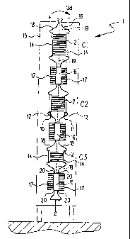
A power converter 1 according to the invention is shown in Fig. 5.
The components of the power converter 1 shown are the components of
the circuit for a phase of the power converter 1 shown in Fig. 2.
The power converter 1 has a housing 15. A capacitor 2 and two
semiconductor power switches 3, combined to form a power switch
unit 16, are alternately arranged above one another in the housing
15. A cooling body 17 each, provided with cooling ribs, is
fastened laterally to the power switch unit 16. The cooling ribs
of the cooling body 17 extend in the same direction as the cooling
channels 14 of the capacitors 2. The dimensions of the capacitors
2 depend essentially on the capacities and on the voltage of the
capacitors 2 and thus also on the number of capacitor elements 9.
Thus, far example, the capacitor C1 is larger than capacitor C2 and
Capacitor C2 is, in turn, larger than capacitor C3.
The modular construction of the power converter 1 can be seen
especially well in Fig. 5. The compact modular construction of the
power converter 1 according to the invention is only possible due
to the structure of the capacitors 2 with a connector pair 10, 11
on the upper side 5 and a further connector pair 10, 11 on the
lower side of the capacitor 2, as described above. The electrical
connection between the connector pairs 10, 11 of the capacitors 2
WO 02/11273 cA o24ooais 2oo2-oa-2i pCT/EP01/06326
11
and connections 20 of the power switch units 16 or a direct-current
network are only made by means of flat low-inductive busbar
conductors 18. The busbar conductors 18 consist of an electrically
conductive material, e.g. of copper, and are air-insulated in the
present embodiment. The use of expensive so-called bus bars, as is
conventional in the prior art, can be omitted in the power
converter 1 according to the invention. In addition to air, the
busbar conductors 18 can of course also be insulated with any other
materials desired.
To avoid a short circuit between two adjacent busbar conductors 18
of an electric connection due to foreign bodies reaching inside the
housing 15 (e.g. forgotten tool, insects, animals) or the like, an
insulating plate 19 can be inserted between two adjacent busbar
conductors 18. The insulating plates 19 are shown in Fig. 5 by a
broken line. They consist of a solid insulator, e.g. of plastic.
The power converter 1 according to the invention makes due with a
minimum of additional low-inductive flat busbar conductors 18 for
connecting the capacitors 2 to the semiconductor power switches 3,
since most of the electrical connections between the capacitors 2
and the power switches 3 are made by the low-inductive contact
paths 8 within the capacitors 2.
The modular construction of the power converter 1 according to the
invention enables an especially cost-effective assembly and
maintenance of the components (in particular the capacitors 2 and
the power switching elements 16) of the power converter 1. The
air-insulated low-inductive flat busbar conductors 18 are
especially durable and can also transport high voltages without
difficulty. Due to his construction, the power converter 1
according to the invention is suitable for use in the mean-
WO 02/11273 cA o24ooais 2oo2-oa-2i pCT/EPOl/06326
12
frequency and high-frequency range. Moreover, the components of
the power converter 1 according to the invention can be cooled
easily and especially effectively with cooling air due to the
modular construction.