Note: Descriptions are shown in the official language in which they were submitted.
CA 02402037 2002-09-04
WO 01/07828 PCT/US00/18002
LIGHTING APPARATUS
Field of the Invention
The present invention relates generally to the field of lighting devices, and
more specifically to devices
capable of a low profile which utilize point sources, such as light emitting
diodes, for illumination.
Description of the Related Art
Low profile lighting devices are useful in a variety of applications, such as
decorative strip lighting or display
panel illumination. One common form of strip lighting utilizes neon tubes.
Neon tubes have the advantages of being
lightweight and lending themselves to decorative lighting. Further, the light
output from neon tubes is relatively diffuse
and uniform in appearance. However, neon tubes are fragile, require high
voltage, and generate significant radio-
frequency (RF) interference, which must often be shielded at significant cost.
Fluorescent lighting is likewise diffuse,
but is generally limited to short lengths and typically includes unattractive
electrical connections.
Display panel illumination is often accomplished by placing light sources
behind the panel to illuminate it. A
diffuser box containing a light source can generate output that is fairly
uniform, so long as the light sources are
sufficiently far away from the display panel. This makes such devices bulky,
however. If the light sources are too
close to the panel, the illumination will no longer be uniform, and the
sources will be seen as "hot spots." Thus there is
a need for a compact lighting device that provides uniform output intensity.
Summary of the Invention
According to one aspect of the invention, an illumination apparatus includes a
cavity having reflective
surfaces and an output area, as well as at least one light source disposed in
the cavity, wherein the light source
includes a point source and an optical diverter having a flared reflecting
surface. The apparatus further includes an
optical conditioning element over the output area, with the optical
conditioning element including at least a diffuser, for
example, a translucent film or plastic sheet. In a preferred embodiment, the
flared surface is curved, and may be
cuspated. In one preferred embodiment, the point source comprises an LED. In a
preferred embodiment, the cavity
reflecting surfaces are diffusively reflective.
According to another aspect of the invention, an illumination apparatus
comprises a housing that includes a
cavity having reflective surfaces and an output aperture. The apparatus also
includes an optical conditioning element
across the output aperture, in which the conditioning element comprises at
least one sheet having a plurality of pixels.
The apparatus further includes at least one light source disposed within the
cavity directly beneath the conditioning
element, in which the (at least one) light source includes a point source
spaced less than 3-1/2 inches from the sheet
that illuminates the reflective surfaces such that the ratio of the luminance
of adjacent pixels is between 0.95 and
1.05 and such that the ratio of the luminance of non-adjacent pixels is
between 0.5 and 2.0, whereby the appearance
of illumination at the sheet is substantially uniform. In a preferred
embodiment, the optical conditioning element
-1-
CA 02402037 2002-09-04
WO 01/07828 PCT/US00/18002
includes a diffuser sheet disposed below the prism sheet. In one preferred
embodiment, the optical conditioning
element includes a second prism sheet with orientation 90 from the first. In
a preferred embodiment, the (at least
one) light source includes a point source and a total internal reflection lens
having a cuspated surface for reflecting
light from the point source against the diffusive reflective surfaces.
According to another aspect of the invention, an illumination apparatus
includes a cavity formed by reflective
material, in which the cavity has an output area. An optical conditioning
element is at the output area. The apparatus
further includes a light source in the cavity, in which the light source
includes a point source and an optical diverter
having a reflecting surface which is partially reflective and partially
transmissive. The reflective surface of the diverter
allows a portion of light incident thereon to pass through the reflecting
surface, while reflecting another portion of the
incident light onto the reflective material of the cavity. The reflective
material reflects light within the cavity, whereby
the output area and the optical conditioning element are illuminated. In a
preferred embodiment, the reflecting surface
of the diverter is comprised of scattering centers which scatter light
incident thereon.
According to yet another aspect of the invention, an illumination apparatus
includes an optical diverter. The
diverter includes transparent material having a reflecting surface formed by a
refractive index interface configured to
totally internally reflect light from a point source positioned to emit a
first portion of light rays towards the reflecting
surface and a second portion of light rays towards a side surface of the
diverter. The diverter includes a refracting
interface that refracts the second portion of light rays towards the
reflecting surface, such that both the first and
second portions of light rays are reflected from the reflecting surface.
According to yet another aspect of the invention, there is provided an optical
diverter that includes
transparent material having a flared reflecting surface formed by a refractive
index interface. The interface is
configured to totally internally reflect light from a point source which is
positioned adjacent to an apex of the flared
reflecting surface and which emits light rays for reflection by the reflecting
surface.
According to a further aspect of the invention, an illumination apparatus
includes a cavity having reflective
surfaces and an output area. The apparatus further includes at least one light
source disposed in the cavity, in which
the light source includes a point source and an optical diverter having a
surface that is partially reflective and partially
transmissive. The apparatus also includes an optical conditioning element over
the output area, in which the optical
conditioning element includes a diffuser, wherein the diverter is positioned
between the point source and optical
conditioning element such that (a) a portion of light emitted by the point
source is reflected from the diverter towards
the reflective surfaces of the cavity, and (b) another portion of light
emitted by the point source is transmitted through
the surface of the diverter towards the optical conditioning element, with the
diverter sized to allow at least a
substantial portion of the reflected light to reach the optical conditioning
element without passing through the diverter,
and wherein the diverter and the reflective surfaces of the cavity are
arranged to allow at least a substantial portion of
the transmitted light to reach the optical conditioning element without
undergoing reflection.
-2-
CA 02402037 2002-09-04
WO 01/07828 PCT/US00/18002
Brief Description of the Drawings
FIGURE 1 shows a first embodiment of a low profile lighting device with the
housing partially cut away to
reveal one of the point light sources and optical diverters therein.
FIGURE 2 is an exploded view of the embodiment illustrated in FIGURE 1.
FIGURE 3 shows another embodiment of a low profile lighting device.
FIGURE 4 is an exploded view of the embodiment illustrated in FIGURE 3.
FIGURES 5A and 5B are end and plan views, respectively, of a mounting channel
having a slot for mounting
the embodiment of FIGURES 1-2 or FIGURES 3-4 to the mounting bracket of
FIGURES 6A and 6B.
FIGURES 6A and 6B are elevation and plan views, respectively, of a mounting
bracket which is secured to a
mechanical structure such as a building, and which receives the mounting
channel of FIGURES 5A and 5B to mount the
low profile lighting device on the building.
FIGURES 7A and 7B show a collar for mechanically and electrically coupling two
lighting devices.
FIGURE 7C shows an electrical arrangement for coupling power to an end of a
lighting device.
FIGURE 8 shows an optical diverter which utilizes total internal reflection
for laterally diverting light from a
light emitting diode or other point source.
FIGURES 9, 10, and 11 show the progression of light rays through the optical
diverter of FIGURE 8.
FIGURE 12 shows an optical diverter which produces highly collimated
"equatorial" output beam.
FIGURE 13 shows the progression of light rays through an optical diverter
having scattering centers on its
top surface for diffusely transmitting some light through the top surface.
FIGURE 14 shows an optical diverter having a roughened surface pattern in the
form of a series concentric
rings on its top surface for diffusely transmitting some light through the top
surface.
FIGURE 15 shows an embodiment of a lighting device in the form of an
alphanumeric character.
Detailed Description of the Preferred Embodiments
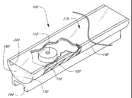
One preferred embodiment of a lighting device 100, illustrated in FIGURE 1,
comprises plural light sources,
each of which includes a point source such as a light emitting diode (LED) 174
shown in FIGURE 8, and an optical
diverter 110. Light from the LED 174 is received by the optical diverter 110,
which redirects the light laterally and
downwardly. The plural LEDs are coupled to each other electrically by a
printed circuit board 130 (a wire harness is an
alternative configuration). The point sources 174 and optical diverters 110
are mounted within an elongate cavity
formed by a sheet 150 of diffusively reflective material in the general form
of a half or hemi cylinder. The sheet 150 is
mounted in, and extends the length of, a housing 140, which may be an
extrusion. The housing 140 is generally
elongate and has a width that is not substantially greater than the width of
the light output area. The printed circuit
board 130 is disposed between the sheet 150 and the bottom of the housing 140.
Wires (not shown) pass through the
sheet 150 to electrically connect the point sources to the circuit board. A
mounting channel 144 may be included on
the bottom of the housing 140 for mounting the device 100 to a building. The
mounting channel 144 may, for
-3-
CA 02402037 2009-03-10
example, be made of acrylic that is bonded or glued to the housing 140, or the
channel 144
may be integrally formed with the housing 140 as part of an extrusion process.
The light that
exits the diverters 110 is reflected by the diffusely reflecting sheet 150,
located between the
optical diverters 110 and the circuit board 130, as well as by diffusely
reflecting end caps 160
connected to the housing 140 at either end of the device 100. If a plurality
of optical diverters
110 are linearly arranged along the longitudinal axis of the cavity, the
maximum separation
between adjacent optical diverters 110 is preferably about twice the width of
the device 100.
Further, the optical diverters 110 are preferably separated by at least 0.5
inches.
The surfaces of the diffusely reflecting sheet 150 and the diffusely
reflecting end caps
160 are preferably matte white, with diffuse reflectivity over 90%, preferably
96% or more, For
this purpose, the sheet 150 and the caps 160 may be coated with diffusely
reflective tape, such
as DRP Backlight Reflector (W. L. Gore & Associates), white paint, or more
exotic materials
such as Labsphere Corporation's Spectraflect paint. The reflectivity of
Spectraflect paint is
98%, which is considerably higher than the reflectivity of house paint, which
is approximately
92%. DRP"' Backlight Reflector has a reflectivity of approximately 97%-99.5%.
Alternatively,
the diffusely reflecting sheet 150 and the diffusely reflecting caps 160 may
be constructed from
a diffusely (or specularly) reflecting material, such as titanium dioxide,
pigmented Lexan'm
polycarbonate, or Spectralon"plastic, thereby avoiding the need to apply a
separate coating to
the sheet 150 and the end caps 160. The reflectivity of Spectralon"'plastic is
about 99%.
Although it is preferred that the reflective surfaces 150,160 be diffusively
reflective, in an
alternative embodiment these surfaces comprise specularly reflecting surfaces
that are
preferably faceted as in a product sold by 3M under the name Visible Mirror
Film (specular or
diffuse). Additionally, while the cavity of the preferred embodiment is gas-
filled (with air), the
cavity may also be formed by a liquid or solid.
Light exits the device 100 through a sheet member or film stack 170, which
faces the
diffusely reflecting sheet 150. As shown in FIGURE 2, the sheet member 170
acts as the
output face of the device 100, and comprises an optical conditioning element
210, which may
be covered with transmissive outer protective cover 200. The optical
conditioning element 210
includes (in the direction of light propagating outward through the sheet
member 170) one or
more sheets of material, which are substantially parallel to each other,
namely, a diffuser 180,
an optional first prism sheet 190, and an optional second prism sheet 194. The
diffuser 180
acts to randomize the direction of the light incident upon it and preferably
has relatively low
backscattering. By way of example, the diffuser 180 may be of any construction
that will diffuse
light, such as translucent sheets of plastic, or plastic with a rough surface.
The prism sheets
4
CA 02402037 2009-03-10
190 and 194 may each be a brightness-enhancing film (BEF) for reducing the
solid angle of the
light, with an angular emission in the range of 50 to 80 degrees full width
half maximum
(FWHM). Brightness-enhancing films suitable for use in the preferred
embodiments are
commercially available from 3M Corporation. A thin film BEF, having linear
pyramidal structures
therein, is described in U. S. Patent 5,684,354 to Gleckman, Preferably, the
repeated
structures of the sheets 190 and 194 are crossed at generally 90 degrees with
respect to each
other, and are each oriented at 45 degrees with respect to the longitudinal
axis of the elongate
housing 140.
4a
CA 02402037 2002-09-04
WO 01/07828 PCT/US00/18002
The diffuser 180 and the prism sheets 190 and 194 of the optical conditioning
element 210 spread the light
uniformly over the output face of the device 100. The prism sheets also serve
to concentrate the optical energy within
a field of view, and this causes the light to be directed more intensely in
the direction of an observer within that field.
While it is preferred that the diffuser 180 be placed below the prism sheets
190 and 194 (as shown in FIGURE 2), it
will be understood that the position of the diffuser and the prism sheets may
be exchanged. The optical conditioning
element 210 and the point source 174 are preferably separated by less than 3.5
inches, more preferably by less than
2.5 inches, and still more preferably by less than 1.5 inches. The protective
outer cover 200 protects the device 100
from the environment, and may act as a color filter or contain darkened or
lightened regions of a specific pattern, such
as a logo, design, or alphanumeric characters.
As shown in FIGURE 2, the point sources 174, such as LEDs, are disposed just
beneath the optical diverters
110. Electrical leads (not shown) from the point sources 174 are connected to
the printed circuit board 130, with the
sheet 150 having holes punched therein for accepting the leads of the LEDs
174, such that the sheet is positioned
between the LEDs and the printed circuit board. The housing 140 includes lips
or flanges 220 for holding the diffusely
reflecting sheet 150 in place. The sheet 150 (and the LEDs 174 and the printed
circuit board 130 to which the sheet
150 is attached) is advantageously flexible so that it may be slid underneath
the lips 220, permitting the sheet 150 to
naturally assume a shape which is typically parabolic in cross section. When
the sheet 150 assumes a parabolic cross
section, light reflected off the sheet is efficiently directed towards the
optical conditioner 210.
An alternative preferred embodiment is illustrated in FIGURES 3 and 4. In this
embodiment, a device 230
includes a cylindrically shaped housing 240 that functions both as a housing
and a protective outer cover. The sheet
member 170 is secured to a pair of lips or flanges 244 that run along the
length of the device 230. (The flanges 244
may also function the same as the lips 220 of FIGURE 2, for holding the
reflecting sheet 150 in place.) The device 230
is otherwise substantially similar to its counterpart 100 of FIGURES 1-2, and
similar parts are designated with the
same reference numerals. The housing 240 may be colored or include darkened
portions for producing a desired visual
effect. Alternatively, separate elements or layers of film (not shown)
disposed between the conditioning element 170
and the housing 240 may be used for achieving a desired optical effect. Such
elements may also be used in
conjunction with the embodiment shown in FIGURES 1 and 2.
One aspect of the embodiments shown in FIGURES 1-2 and FIGURES 3-4 is that the
intensity of light exiting
the optical conditioning element 210 is spatially very uniform and thus
appears to an observer to have constant
luminance across the entire element 210. This uniformity can be quantified
with reference to an imaginary grid of 1
mm2 "pixels" on the output side of the optical conditioning element 210. As
used herein, the term "pixel" means any
square millimeter cell defined by an imaginary grid an the output side of the
element 210 formed by two orthogonal
sets of parallel lines separated by 1 mm. Thus, a pixel as used herein does
not represent a discrete element, but rather
corresponds to a square millimeter of the exterior surface of element 210. The
ratio of the luminance of adjacent
pixels is preferably between 0.95 and 1.05, more preferably between 0.98 and
1.02, and still more preferably between
0.99 and 1.01. The ratio of the luminance of non-adjacent pixels is preferably
between 0.5 and 2.0, more preferably
-5-
CA 02402037 2002-09-04
WO 01/07828 PCT/US00/18002
between 0.57 and 1.75, still more preferably between 0.67 and 1.5, and most
preferably between 0.77 and 1.3. It
will be understood that a given ratio can be more or less than 1.0, depending
upon whether the ratio is determined with
the intensity of the more intense pixel placed in the numerator or the
denominator, respectively.
As illustrated in FIGURES 5A and 5B, the mounting channel 144 is configured to
mate with a mounting
bracket 250, such as that illustrated in FIGURES 6A and 6B. The mounting
bracket 250 is attached to a plate 260
that may be fastened to a building 270 or other structure using screws 280,
bolts or the like. The mounting bracket
250 may be made of compliant plastic (or another suitable, outdoor-rated
material) and comprises a latching member
290. To secure the mounting bracket 250 to the mounting channel 144, the
profile of the latching member 290 is
reduced by pressing the latching member 290 into the mounting channel 144,
thereby squeezing both sides of the
latching member about a slot 300, so that the latching member 290 is received
by the mounting channel 144. Once
the latching member 290 is within the channel 144, it springs back to reassume
its uncompressed state (FIGURE 6A),
thereby holding the lighting device 100 (230) in place.
The lighting devices 230 (100) may be advantageously constructed in segments
of various lengths, such as
2, 4, or 8 feet. Two or more segments may be coupled together by a collar 310
as illustrated in FIGURES 7A and 7B.
Within the collar 310 is a dual female connector 320 for receiving respective
male connectors 330 from each of two
lighting devices 230. The male connectors 330 are electrically connected to
the printed circuit board 130, and the
female connector 320 is tied electrically to a power source via an electrical
line 340. The female connector 320 may
be held in place within the collar 310 by, for example, rings or spokes (not
shown) that extend within the collar.
FIGURE 7C shows an alternative arrangement in which power is supplied via a
single female connector 360 located at
one end of one of the devices 230. In this case, adjacent devices 230 may be
connected by a dual female connector
(not shown) to which no electrical line 340 is attached.
A preferred embodiment of the optical diverter 110 is illustrated with respect
to FIGURES 8-11. FIGURE 8
shows a cross section of an optical diverter 110a which includes a total
internal reflection (TIR) region 400 with a
surface 410 that is smoothly curved and defines a vortex shape forming an apex
421 that extends into the optical
diverter 110a. The optical diverter 110a is surrounded by air, so that a
refractive index interface is formed, which
permits total internal reflection. The surface 410 of this embodiment
substantially completely reflects light incident
thereon, such that substantially no light is transmitted therethrough. The TIR
region 400 may advantageously have
the shape of an equiangular spiral that forms a cuspate portion 420. The
surface 410 of FIGURE 8 is shown as being
axially and circularly symmetrical and extending 360 degrees about a vertical
axis 424 aligned with and passing
through the point source 174. However, a TIR diverter (not shown) may be used
in which the cuspate portion is
symmetrical about a line rather than being symmetrically oriented about a
point, as in FIGURE S. Such a TIR diverter
enjoys planar rather than radial symmetry.
In the embodiment of FIGURE 8, the point source 174, such as an LED, is
mounted below the apex 421 of the
TIR surface (i.e., just below the point on the cusp 420) in close proximity
thereto, with the reflecting surface extending
360 about the LED and apex. The LED 174 is contained within an LED package
430, which resides within a recess
-6-
CA 02402037 2002-09-04
WO 01/07828 PCT/US00/18002
440 in the optical diverter 110a. In order to ensure good coupling into the
optical diverters 110 disclosed herein, and
to reduce reflections at the interface between the LED package 430 and the
boundary of the recess 440, a transparent
optical coupling agent (not shown), such as an adhesive or gel, may be used to
preclude any optically interfering air
gaps between the LED 174 and the optical diverter. The transparent optical
coupling agent could be an epoxy, silicone,
or any well-known organic or inorganic optical coupling material. Preferably,
the refractive index of the coupling agent
is between that of the LED package and the optical diverter 110.
The surface 410 may be curved, or it may include a plurality of flat surfaces
approximating a curve to form a
totally internally reflecting (TIR) lens having a focal point. When the point
source 174 is positioned (as shown) at this
focal point, light generated by the point source 174 is totally internally
reflected from the surface 410. If the surface
410 is curved, any one of a number of shapes may be employed, such as a
hyperboloid, paraboloid, cone, cusp or other
surface of revolution. Mathematical modeling of these shapes can be performed
with an optical analysis software
package such as ASAP by Breault Research of Tucson, Arizona. The surface 410
is contoured such that substantially
all light rays emitted from the LED 174 at the focal point of surface 410 are
incident on the surface 410 at an angle at
least equal to the critical angle. This may be accomplished by calculating the
range of possible incidence angles of
light rays from the LED 174 at the focal point at various local portions of
the surface 410. The local portions are then
oriented so that all rays are incident within the critical range. The local
portions could be large in size so that the
surface 410 consists of a collection of flat surfaces, for example. As the
size of the local portion decreases, the
surface 410 forms into a smoothly curved surface having, for example, the
equiangular spiral shape shown in FIGURE
8.
While a circularly and axially symmetric cuspated surface is preferred for
many applications, the surface 410
need not be symmetrical. In general, the surface 410 is flared so that light
that reflects off of the surface 410 will be
directed out of and away from the optical diverter 110a. In this sense, the
optical diverter 110a of this embodiment
acts as a lateral diverter of light. This flared surface 410 may be viewed as
extending between an apex portion of the
surface 410 (corresponding to the cusp 420 of FIGURE 8) and a base portion 450
above the apex. The base portion
450 flares outwardly (radially) from the vertical axis 424 that passes through
the apex 421 and the point source 174.
Thus, the flared reflecting surface 410 flares outwardly from the apex 421 to
the base portion 450. A groove 480 in
the embodiment of FIGURE 8(and the embodiments of FIGURES 9, 10, 11 and 13
discussed below) has a depth such
that substantially all rays which would otherwise propagate directly from the
point source 174 to the side surface 120
of the diverter 110a are intercepted by at least one wall of the groove. Thus,
the groove 480 prevents direct
propagation of rays though the side surface 120 and onto the optical
conditioning element 210, and thereby prevents
such rays from causing non-uniformities in the output luminance.
FIGURES 9-11 depict the optical paths of various rays within the optical
diverter 110a, in which FIGURE 9 is
an overview of the various paths that light rays take. The optical diverter
110a is illustrated as having an annular
groove 480, one face of which (surface 490) is frosted. The groove 480
redirects light from the LED 174 that is
incident thereon. Light rays emanate from the LED 174 at the focal point of
surface 410 within the LED package 430.
-7-
CA 02402037 2002-09-04
WO 01/07828 PCT/US00/18002
Some light rays 460 are refracted through the inner side surface of the grove
480 for propagation to the top surface of
the groove, where the rays 460 are again refracted for propagation to the TIR
reflecting surface 410. Other rays 470
pass within the region bounded by the inner side surfaces of the groove 480,
and thus by-pass the groove for direct
propagation to the TIR reflecting surface. Rays 460 and 470 both undergo TIR
at surface 410, are reflected
downwards, and eventually exit the diverter through side surface 120. As
discussed above in connection with FIGURE
1, light exiting the diverter 110a is diffusely reflected by the sheet 150 and
by the end caps 160 at either end of the
device 100 (230), and eventually exits the device through the sheet member
170, which faces the diffusely reflecting
sheet 150.
The progress of light rays 460 and 470 though the diverter 110a is shown in
more detail in FIGURES 10 and
11, respectively. FIGURE 10 shows light rays 460 being refracted by the walls
of the groove 480. While some rays
460a pass directly out of the side surface 120 of the diverter 110a after
undergoing TIR, other rays 460b are
internally reflected towards the frosted surface 490, where they are scattered
in many directions before exiting the
device 100 (230). FIGURE 10 also shows rays 465, which pass through the inner
side surface of the groove 480 for
propagation to the frosted outer side surface 490, where the rays 465 are
scattered in many directions. This
scattering prevents them from becoming visible through the output area. FIGURE
11 shows light rays 470 undergoing
TIR at surface 410 and being refracted at face 120, whereupon the rays 470
exit the diverter 110a. Surface 410 can
have a shape tailored to cause uniform illumination of the sheet 150.
Another TIR embodiment is illustrated in FIGURE 12, in which an optical
diverter 110b includes a flared
reflecting surface formed by a cuspate portion 492 and a refracting portion
formed by an elliptical drum lens or torus
portion 494, below the cuspate portion 492. Both the cuspate portion 492 and
the refracting portion 494 are
surfaces of revolution about an axis 496 that passes through the point source
174, as well as through the apex of the
cuspate portion 492. Light rays 498 that strike surface 410b in the cuspate
portion 492 undergo total internal
reflection and exit the diverter 110b propagating nominally perpendicular to
the axis 496. Light rays 500 exiting a
surface 502 of the toroidal portion 494 are refracted so that they also
propagate nominally perpendicular to the axis
496. Further, the surface 502 is designed so that substantially no rays
propagate from the point source 174 through
the side surface 1 20N without first undergoing TIR at surface 410b. The
resultant distribution of light outside of the
diverter 110b is such that the embodiment of FIGURE 12 acts with an isotropic
hemispheric source to produce an
equatorial distribution with a latitudinal beam width depending on the
relative size of the point source 174. The
diverter 110b is suitable for use in the lighting devices disclosed herein,
but alternatively, it may be used by itself
outside of a housing 140 (240) to produce 360 degree, latitudinally narrow
output in the far field. Typical applications
are aircraft warning beacons for high structures and marine beacon on buoys.
Although the embodiment illustrated in FIGURES 8-11 includes a surface 410
that is totally internally
reflecting with respect to light rays 460 and 470, and the embodiment of
FIGURE 12 also includes a surface 410b that
is totally internally reflecting, an alternate embodiment comprises a surface
510 which is only partially rather than
totally internally reflecting. As illustrated in FIGURE 13, this embodiment
includes a flared surface comprising a
-8-
CA 02402037 2002-09-04
WO 01/07828 PCT/US00/18002
cuspate portion 420c and a base portion 450c. Optical radiation 520 that would
otherwise be reflected for
propagation through the side face 120 of the optical diverter 110c passes
through (i.e., is diffusely transmitted by) the
surface 510 for propagation directly through the sheet member 170, without
reflecting off the reflective sheet 150 or
one of the caps 160. fihis may enhance uniformity of illumination of the sheet
member 170 and eliminate optical
losses associated with reflections off the sheet 150 and the caps 160. In
FIGURE 13, however, a substantial portion
of the light rays 460 and 470 are preferably still totally internally
reflected at surface 510. The optical diverter 110c
may be advantageously sized to allow at least a substantial portion of the
light reflected off the cavity sheet 150 to
reach the optical conditioning element 210 without passing through the
diverter 110c, and the reflective surfaces 150
and 160 arranged to allow at least a substantial portion of the light
transmitted through the surface 510 to reach the
optical conditioning element without reflection. This feature acts to
compensate for reduced illumination of the sheet
150 just beneath the diverter 110c.
A surface 510 that is partially reflecting and partially transmitting may, in
general, be formed by
appropriately selecting the angle of incidence between the light rays 460
(470) and the surface 190. For example, the
surface 510 may be formed at an angle that insures that some light "leaks
through" the surface 190 while other light
is reflected off of surface 190. Additionally, the apex of the cuspated
portion may be rounded to provide controlled
leakage of light from the LED 174 through the surface 510 immediately above
the LED. This eliminates dark spots
above the LED 174. Moreover, as illustrated in FIGURE 13, a surface 410 that
is initially totally internally reflecting
may be lightly sandblasted or etched to form distributed scattering centers
530 thereon, such that some of the light
incident on the scattering centers passes through the surface 410. These
scattering centers 530 may be distributed
non-uniformly on the surface 410. Also, the surface 410 may be heavily etched
or sandblasted to form a pattern such
as a series of concentric rings 540 (see the diverter 110d of FIGURE 14) about
a center 544 at an apex of the surface,
which likewise results in some of the light leaking through the surface.
The optical diverters shown in FIGURES 8-14 may be comprised of material that
is transparent to the light
produced by the LED 174, such as a transparent polymeric material, and may be
manufactured by various well-known
methods, such as machining or injection molding. Preferred materials for the
optical diverters 110 are acrylic,
polycarbonate, and silicone. Acrylic, which has an index of refraction of
approximately 1.5, is scratch-resistant and
has a lower cost relative to polycarbonate. On the other hand, polycarbonate,
which has an index of refraction of
approximately 1.59, has higher temperature capabilities than acrylic.
Polycarbonate also has improved mechanical
capabilities over acrylic. Silicone has a refractive index of approximately
1.43. The refractive index of air is nearly
1Ø
While the reflectors of the preferred embodiments are flared, another
embodiment (not shown) utilizes a non-
flared planar reflector which is partially reflective and partially
transmissive. Also, instead of using optical diverters
110 which rely upon total or partial internal reflection, reflection may be
provided by partially or totally reflective
mirrors (not shown), in which the mirrors are preferably contoured to reflect
light laterally. Such mirrors may
advantageously include a curved surface, so that light is reflected over a
range of angles and scattered within the
-9-
CA 02402037 2002-09-04
WO 01/07828 PCT/US00/18002
device 100 (230) to provide uniform illumination of the sheet member 170. This
function may also be performed by a
transparent optical element that has a non-uniform change in its index of
refraction, for example, a gradient index
optical element.
The point sources 174 may advantageously comprise an LED cluster that provides
tricolor output, e.g., red,
green, and blue, so that virtually any color may be produced by appropriately
selecting the relative intensity of the
respective component wavelengths. Further, both gradual and fast time-changes
in color are possible, and travelling
wave patterns may be generated when the respective outputs of the LEDs 174 are
successively varied in a coordinated
fashion. Although the point sources 174 have been principally described with
respect to LEDs, other point sources
may be used, such as miniature incandescent filaments or arc lamps (not
shown). However, LEDs are preferred
because of their ability to operate at relatively low voltage (e.g., 24 volts
DC or less). Also, LEDs generate no RF
interference. As a further alternative to using LEDs as the point sources 174,
a fiber optic line (not shown) may be
used to distribute light to a series of optical diverters 110, in which light
is tapped off at various points along the fiber
optic line (corresponding to the point sources 174) and is directed into the
diverters. In this case, a laser diode or other
light generator may be used to couple light into the fiber optic line, and the
fibers form the point sources of light.
The cylindrical or semi-cylindrical devices illustrated in FIGURES 1-4 may be
used in a number of different
applications, such as for decorative illumination, light boxes, backlights,
and for guidance along pathways. Further, the
housing utilized with the optical diverters 110 and sheet member 170 may be
constructed in various sizes and shapes,
including wide area planar, linear elongate, and curved elongate. FIGURE 15
illustrates one embodiment in which the
letter "G" has been formed. Other possible embodiments will be apparent to
those skilled in the art. For example,
instead of positioning the optical diverters 110 along a line or a curve, the
optical diverters may be mounted, for
example, in a grid (not shown) to cover a wide-area display, the surface of
which may have numbers, letters, logos, or
other indicia printed thereon.
It should be understood that the scope of the present invention is not limited
by the illustrations or the
foregoing description thereof, and that certain variations and modifications
of the foregoing embodiments will suggest
themselves to one of ordinary skill in the art.
-10-