Note: Descriptions are shown in the official language in which they were submitted.
CA 02402556 2002-09-11
WO 01/69722 PCT/GBOI/00997
DIELECTRIC RESONATOR ANTENNA ARRAY WITH STEERABLE
ELEMENTS
The present invention relates to arrays of dielectric resonator antennas
(DRAB) in
which the patterns of the individual DRA elements may be electronically
steered in
synchronism with the array pattern.
Since the first systematic study of dielectric resonator antennas (DRAs) in
1983
[LONG, S.A., McALLISTER, M.W., and SHEN, L.C.: "The Resonant Cylindrical
Dielectric Cavity Antenna". IEEE Transactions on Antennas and Propagation, AP-
31,
1983, pp 406-412], interest has grown in their radiation patterns because of
their high
radiation efficiency, good match to most commonly used transmission lines and
small physical size [MONGIA, R.K. and BI-IARTIA, P.: "Dielectric Resonator
Antennas - A Review and General Design Relations for Resonant Frequency and
Bandwidth", International Journal of Microwave and Millimetre-Wave Computer-
Aided Engineering, 1994, 4. (3), pp 230-247].
The majority of configurations reported to date have used a slab of dielectric
material
mounted on a ground plane excited by either an single aperture feed in the
ground
plane [ITTIPIBOON, A., MONGIA, R.K., ANTAR, Y.M.M., BHARTIA, P. and
CUHACh M: "Aperture Fed Rectangular and Triangular Dielectric Resonators for
use as Magnetic Dipole Antennas", Electronics Letters, 1993, 29. (23), pp 2001-
2002] or by a single probe inserted into the dielectric material [McALLISTER,
M.W., LONG, S.A. and CONWAY G.L.: ''Rectangular Dielectric Resonator
Antenna", Electronics Letters, 1983, 19, (6), pp 218-219]. Direct excitation
by a
transmission line has also been reported by some authors [KRANENBURG, R.A.
and LONG, S.A.: "Microstrip Transmission Line Excitation of Dielectric
Resonator
Antennas", Electronics Letters, 1994, 24, (18), pp I 156-1157].
The concept of using a series of these single feed DRAs to build an antenna
array has
already been explored. For example, an array of two cylindrical single-feed
DRAs
has been demonstrated [CHOW, K.Y.; LEUNG, K.W., LUK, K.M. AND YUNG,
E.K.N.: "Cylindrical dielectric resonator antenna array', Electronics Letters,
1995;
31. (18), pp 1536-1537] and then extended to a square matrix of four DRAB
[LEUNG, K.W., LO, H.Y., LUK, K.M. AND YUNG, E.K.N.: ''Two-dimensional
cylindrical dielectric resonator antenna array", Electronics Letters, 1998,
34, (13), pp
1283-1285]. A square matrix of four cross DRAB has also been investigated
CA 02402556 2002-09-11
WO 01/69722 PCT/GB01/00997
[PETOSA, A., ITTIPIBOON, A. AND CUHACI, M.: "Array of circular-polarized
cross dielectric resonator antennas", Electronics Letters, 1996, 32, (19), pp
1742-
1743]. Long linear arrays of single-feed DRAB have also been investigated with
feeding by either a dielectric waveguide [BIRAND, M.T. AND GELSTHORPE,
R.V.: "Experimental millimetric array using dielectric radiators fed by means
of
dielectric waveguide", Electronics Letters, 1983, 17, (18), pp 633-635] or a
microstrip [PETOSA, A., MONGIA, R.K., ITTIPIBOON, A. AND WIGHT, J.S.:
"Design of microstrip-fed series array of dielectric resonator antennas",
Electronics
Letters, 1995, 31, (16), pp 1306-1307]. This last research group have also
found a
method of improving the bandwidth of microstrip-fed DRA arrays [PETOSA, A.,
ITTIPIBOON, A., CL'HACI, M. AND LAROSE, R.: "Bandwidth improvement for
microstrip-fed series array of dielectric resonator antennas", Electronics
Letters,
1996, 32, (7), pp 608-609]. It is important to note that none of these
publications
have discussed the concept of mufti-feed DRAB or the concept of array element
steering.
Earlier work by the present inventors [KINGSLEY, S.P. and O'KEEFE, S.G., "Beam
Steering and Monopulse Processing of Probe-Fed Dielectric Resonator Antennas",
IEE Proceedings - Radar, Sonar and Navigation, 146, 3, 121 - 125, 1999] shows
how
several spatially separated feeds can be used to drive a single circular slab
of
dielectric material so as to produce an antenna with several beams facing in
different
directions. The simultaneous excitation of several feeds means that the DRA
can
have electronic beamsteering and direction finding capabilities. This work is
also
disclosed in the present applicants US patent application serial no 09/431,548
entitled
"Steerable-beam multiple-feed dielectric resonator antenna", the disclosure of
which
is incorporated into the present application by reference.
The present application extends the previous work of Kingsley and O'Keefe by
considering the properties and benefits of arrays composed of many such mufti-
feed
DRAB. A wide range of array geometries is considered.
An antenna array is a collection of (often evenly spaced) simple elements such
as
monopoles, dipoles, patches, etc. The arrangement of elements to form the
array may
be linear, 2-D, in a circle, etc. and the shape of 2-D arrays may be
rectangular,
circular, oval, etc. In an array, each individual element has a broad
radiation pattern
but when they are combined together, the array as a whole has a much narrower
radiation pattern. More importantly, by feeding the elements with different
phases or
2
CA 02402556 2002-09-11
WO 01/69722 PCT/GBO1/00997
time delays, the array pattern can be steered electronically. This is a most
useful
facility in radar and communications.
It is important to distinguish between the various radiation patterns referred
to in the
present application. Firstly, each element of the array has its own notional
radiation
pattern when considered in isolation. This element pattern may be considered
to be
analogous to the diffraction pattern of one of the light sources in a Young's
slits
interference demonstration. Secondly, the array as a whole has a notional
radiation
pattern, known as the array factor, which is the sum of the idealised
isotropic element
patterns, and which may be considered to be analogous to the interference
pattern in a
Young's slits demonstration. Finally, the actual radiation pattern formed by
the
antenna array, known as the antenna pattern, is the product of the element
patterns
and the array factor. Each of the element pattern, array factor and antenna
pattern
may be considered to have a direction in which transmission/reception has a
maximum gain, and embodiments of the present invention seek to steer these
directions in useful ways.
The radiation patterns of the individual elements of an array are fixed so
that when
the array factor faces straight ahead (on boresight), the resultant antenna
pattern has
the benefit of the full gain of each individual element. In fact, the gain of
the array is
the sum of the gain of the elements. However. when the array factor is steered
off
boresight, the gain can fall because the array factor is moving outside the
pattern of
the individual elements. The only time this is not true is when the elements
are
omnidirectional in the plane of the array (such as monopoles), but as these
are usually
low gain elements there still remains a problem of low gain overall.
Embodiments of the present invention seek to provide an array of dielectric
resonator
antenna elements, where each element has several energy feeds connected in
such a
way that the radiation pattern of each element can be steered. One method of
electronically steering an antenna element pattern is to have a number of
existing
beams and to switch between them or, alternatively, to combine them so as to
achieve
the desired beam direction. The general concept of deploying a plurality of
probes
within a single dielectric resonator antenna, as pertaining to a cylindrical
geometry. is
described in the paper KINGSLEY, S.P. and O'KEEFE, S.G., "Beam Steering and
Monopulse Processing of Probe-Fed Dielectric Resonator Antennas", IEE
Proceedings - Radar, Sonar and Navigation, 146, 3, 121 - 125, 1999, the
disclosure of
which is incorporated into the present application by reference.
3
CA 02402556 2002-09-11
WO 01169722 PCT/GBO1/00997
It has been noted by the present applicants that the results described in the
above
reference apply equally to DRAs operating at any of a wide range of
frequencies, for
example from lMHz to 100,000MHz and even higher for optical DRAs. The higher
the frequency in question, the smaller the size of the DRA, but the general
beam
patterns achieved by the probe/aperture geometries described hereinafter
remain
generally the same throughout any given frequency range. Operation at
frequencies
substantially below IMHz is also possible, using dielectric materials with a
high
dielectric constant.
According to a first aspect of the present invention, there is provided an
array of
dielectric resonator antenna elements, each element being composed of at least
one
dielectric resonator, and a plurality of feeds for transferring energy into
and from the
elements, wherein the feeds of each element are activatable either
individually or in
combination so as to produce at least one incrementally or continuously
steerable
element beam which may be steered through a predetermined angle, and wherein
the
element beams from the elements may be combined so as to form at least one
array
beam which may also be steered through a predetermined angle.
According to a second aspect of the present invention, there is provided an
array of
dielectric resonator antenna elements, each element being composed of at least
one
dielectric resonator associated with a grounded substrate, a plurality of
feeds for
transferring energy into and from the elements. wherein the feeds of each
element are
activatable either individually or in combination so as to produce at least
one
incrementally or continuously steerable element beam which may be steered
through
a predetermined angle, and wherein the element beams from the elements may be
combined so as to form at least one array beam which may also be steered
through a
predetermined angle.
According to a third aspect of the present invention, there is provided an
array of
dielectric resonator antenna elements. each element being composed of at least
one
dielectric resonator associated with a grounded substrate, a plurality of
feeds for
transferring energy into and from the dielectric resonator elements, wherein
the feeds
of each element are activatable either individually or in combination so as to
produce
at least one incrementally or continuously steerable beam which may be steered
through a predetermined angle.
4
CA 02402556 2002-09-11
WO 01/69722 PCT/GBO1/00997
The array may be provided with electronic circuitry adapted to activate the
feeds
either individually or in combination so as to produce at least one
incrementally or
continuously steerable beam which may be steered through a predetermined
angle.
The array may additionally be provided with further electronic circuitry
adapted to
activate each of the antenna elements with a pre-determined phase shift or
time delay
so as to generate an array factor which may be steered through a predetermined
angle.
For example, for a given array factor direction (which here is the same as the
antenna
beam direction), each element may be fed with a different phase or time delay
(and,
in practice, a different amplitude) so that when the element patterns are
added
together, they give rise to an antenna pattern in a predetermined direction.
For a
different antenna beam direction, the phases and amplitudes of the element
feeds will
be different.
By providing an array of steerable DRAs, the present invention seeks to enable
the
individual element patterns to be steered in synchronism with the array factor
as a
whole, thereby forming an array having maximum or at least improved element
gain
for a given array factor direction.
The elements of the array may be arranged in a substantially linear formation,
and
may be arranged side by side so as to provide azimuth beamsteering or one on
top of
the other so as to provide elevation as well as azimuth beamsteering. The
elements
may or may not be evenly spaced, depending on requirements, and the linear
array
may be arranged so as to be conformal to a curved or distorted surface. This
latter
feature has potentially important implications in, for example, communications
on
aircraft. For example, by conforming a linear array of elements to the
fuselage of an
aircraft and by arranging for the element beam patterns all to face the same
way
regardless of the actual orientation of the elements on the fuselage, it is
possible to
match an array beam pattern with the element beam pattern so as to improve
gain.
Furthermore, a dielectric lens may be provided so as to improve control of
azimuth
and/or elevation beamsteering.
Alternatively, the elements of the array may be disposed in a ring-like
formation,
such as a circle, or may be disposed more generally in at least two dimensions
across
a surface. The elements may or may not be evenly spaced, and may, for example,
be
in the form of a regular lattice. As discussed above, the surface in which the
elements are disposed may be conformed to a curved or distorted surface, such
as the
5
CA 02402556 2002-09-11
WO 01/69722 PCT/GBO1/00997
fuselage of an aircraft, and the elements may be individually controlled so
that the
element beam patterns all face the same way regardless of the individual
physical
orientations of the elements themselves. Furthermore. a dielectric lens may be
provided so as to improve control of azimuth and/or elevation beamsteering
Alternatively., the elements of the array may be arranged as a three
dimensional
volumetric array, the array as a whole having an outer envelope in the form of
a
regular solid (e.g. sphere, tetrahedron, cube, octahedron, icosahedron or
dodecahedron) or an irregular solid. The elements may or may not be evenly
spaced,
and may, for example, be in the form of a regular lattice. The volumetric
array may
be formed as a combination of linear and/or surface arrays stacked one on top
of the
other so as to allow both azimuth and elevation beamsteering. Furthermore, a
dielectric lens may be provided so as to improve control of azimuth and/or
elevation
beamsteering.
Beamsteering in elevation is achieved by stacking the DRA elements on top of
each
other, or by forming a stack of DRA arrays, and by energising the elements
appropriately. For example, in a vertical stack of cylindrical multi-probe
elements,
each element on its own can steer an element beam in azimuth, and it is
possible to
feed the probes so that all of the elements form element beams which face in
the
same direction. When combined, these element beams form a horizontal beam in
the
chosen direction which is smaller in elevation than the elevation pattern of a
single
element. By changing the phasing, for example, between the element feeds, it
is
possible to move the combined beam up and down in elevation. In a more complex
system, there may be provided a vertical stack of linear element arrays.
Advantageously, the antenna array as a whole is adapted to produce at least
one
incrementally or continuously steerable beam, which may be steered through a
complete 360 degree circle.
Advantageously, each individual element of the antenna array is also adapted
to
produce at least one incrementally or continuously steerable beam, which may
be
steered through a complete 360 degree circle.
Advantageously, there is additionally or alternatively provided electronic
circuitry to
combine the feeds of each individual element of the antenna array such that
the
element pattern is steered in angle in synchronism with the antenna array
pattern.
6
CA 02402556 2002-09-11
WO 01/69722 PCT/GBO1/00997
Advantageously, there is additionally or alternatively provided electronic
circuitry to
provide at least two feeds to each individual element of the antenna array
such that.
when the array is used to form at least two array factors simultaneously, the
elements
are activatable so as to form at least two element beams simultaneously which
are
steerable in synchronism with the antenna pattern (which is the sum of the at
least
two array factors).
Generally, the at least two array factors together form an antenna pattern
having two
main lobes.
When a conventional antenna array is used to form at least two beams
simultaneously, then at least two sets of phases and amplitudes for the
elements must
be combined by driving each element through one (or more) power sputter!
combiners which are large, lossy devices. Embodiments of the present invention
can
achieve the same result by simply connecting one set of phases and amplitudes
to one
particular feed to each DR.A element and another set of phases and amplitudes
up a
different feed to each element.
The feed to each element may include a cable, fibre optic connection, printed
circuit
track or any other transmission line technique, and these may be of
predetermined
different effective lengths so as to insert different time delays in the feed
to each
element, thus providing beamsteering control. The delays may be controlled and
varied by controlling and varying the effective lengths of the transmission
lines.
either electrically, electronically or mechanically, for example by switching
additional lengths of transmission line in and out of the base transmission
lines.
Alternatively or in addition, beamsteering may be effected by individually
adjusting
the phase of the feed to each element, for example by including diode phase
shifters.
ferrite phase shifters or other types of phase shifters into the transmission
lines.
Additional control may be achieved by varying the amplitude of signals in the
transmission lines, for example by including attenuators therein.
The feed mechanisms to the elements may incorporate a resistive beamforming
matrix of phase shifters so as to insert different phase delays in the feed to
each
element. Alternatively or in addition, the feed mechanisms to the elements may
incorporate a matrix of hybrids, such as a Butler matrix, so as to form a
plurality of
7
CA 02402556 2002-09-11
WO 01/69722 FCT/GBO1/00997
beams from a plurality of elements. A Butler matrix is a parallel RF beam-
forming
network that forms N contiguous beams from an N-element array. The network
makes use of directional couplers, fixed phase differences and transmission
lines. It
is lossless apart from the insertion loss of these components. Other types of
RF
beamforming networks also exist.
Alternatively or in addition. a "weighting" or ''window" function may be
applied
electronically or otherwise to the feeds to the elements so as to control
array factor
sidelobes. Exciting all elements equally gives a uniform aperture distribution
that
results in high array factor sidelobe levels. Applying a window function, such
that
the elements towards the edge of the array contribute less to the array factor
than
those at the centre, can reduce these sidelobe levels.
Alternatively or in addition, an ''error"' or ''correction" function may be
applied
electronically or otherwise to the feeds of the elements so as to control
embedded
element, mutual coupling, surface wave and other perturbing effects. Simple
array
theory assumes that all the elements behave identically. However. those
disposed
toward the edge of an array may behave differently to those nearer the
centre,. because
of the reasons given above. For example, an element at the centre experiences
mutual coupling to the elements either side, but an element at the edge has no
neighbour on one side. These error effects can be measured and corrected for
by
applying a correction factor.
Each element of the array may be connected to a single beamforming mechanism
so
as to produce a single array factor, or to a plurality of beamforming
mechanisms so as
simultaneously to produce a plurality of array factors.
The elements of the array may be disposed so as to permit various
polarisations to be
achieved, such as vertical, horizontal. circular or any other polarisation,
including
switchable .or otherwise controllable polarisations. For example, MONGIA,
R.K.,
ITTIPIBOON, A., CUHACI, M. and ROSCOE D.: "Circular Polarised Dielectric
Resonator Antenna", Electronics Letters, 1994, 30, (17), pp 1361-1362; and
DROSSOS, G., WU, Z. and DAMS, L.E.: "Circular Polarised Cylindrical Dielectric
Resonator Antenna", Electronics Letters, 1996, 32, (4), pp 281-283.3, 4, the
disclosures of which are incorporated into the present application by
reference,
describe how two probes fed simultaneously in a circular cross-section
dielectric slab
and installed on radials at 90° to each other can create circular
polarisation when fed
8
CA 02402556 2002-09-11
WO 01/69722 PCT/GBO1/00997
in anti-phase. Furthermore. DROSSOS, G., WU, Z. and DAMS, L.E.: "Switchable
Cylindrical Dielectric Resonator Antenna", Electronics Letters. 1996. 32,
(10), pp
862-864, the disclosure of which is also incorporated into the present
application by
reference, describes how polarisation may be achieved by switching the probes
on
and off.
Advantageously, there is additionally or alternatively provided electronic
circuitry or
computer software such that when digital beamforming techniques are used, the
feeds
of each individual element of the antenna array are controlled in such a way
that the
element pattern is steered in angle in synchronism with the array factor.
When each element of the array is connected to a separate transmitter module,
a
separate receiver module or a separate transmitter/receiver module. then
digital
beamforming techniques may be used to form steerable array factors of any
desired
shape which are steerable both in azimuth as well as in elevation.
With a conventional array (analogue beamsteering), a single transmitter or
receiver is
distributed to each element with the appropriate phase and amplitude
modifications
along each path. With digital beamforrning, each element has its own
transmitter or
receiver and is instructed by a computer to form the appropriate phase and
amplitude
settings. In the receiving case, each receiver has its own A/D converter, the
outputs
of which can be used to form almost any desired beam shape, many different
beams
simultaneously. or even be stored in the computer and the beams formed some
time
later.
Many such array factors may be formed simultaneously by digital beamforming
techniques through appropriate electronic or software control. Such array
factors
may contain one or more nulls in order to cancel interference, multipath or
other
unwanted signals in given directions. Alternatively, the DRA element pattern
may be
arranged so as to cancel some or all of the unwanted signals. For example,
where a
digital beamforming array has N elements then it generally has N-1 degrees of
freedom, and so may be able to null out jamming signals from N-1 different
directions. In embodiments of the present invention, each DRA element may also
have at least one null in its radiation pattern, and this may be used to null
out
jamming signals from at least one additional direction. Digitally beamformed
array
patterns may be formed on-line in real time or, in the case of recorded
received data,
off line at a later time.
9
CA 02402556 2002-09-11
WO 01/69722 PCT/GBO1/00997
Preferably, the array pattern steering and the synchronous element pattern
steering is
carried out through a complete 360 degree circle.
In one embodiment of the present invention, the dielectric resonator elements
may be
divided into segments by conducting walls provided therein, as described, for
example, in USSN 09/431,548 and in more detail in the present applicant's co-
pending UK patent application no 0005766.1 filed on 11 'h March 2000 and
International patent application no PCT/GBO1/00929, filed on 2°d March
2001, both
entitled "Mufti-segmented dielectric resonator antenna", the full disclosures
of which
are incorporated into the present application by reference.
In a further embodiment of the present invention, there may additionally be
provided
at least one internal or external monopole antenna or any other antenna
possessing a
circularly symmetrical pattern about a longitudinal axis, which is combined
with at
least one of the dielectric resonator antenna elements so as to cancel out
backlobe
fields or to resolve any front-to-back ambiguity which may occur with a
dielectric
resonator antenna having a cosine or figure-of eight radiation pattern. The
monopole
or other circularly symmetrical antenna may be centrally disposed within the
dielectric resonator element or may be mounted thereupon or therebelow and is
activatable by the electronic circuitry. In embodiments including an annular
resonator with a hollow centre, the monopole or other circularly symmetrical
antenna
may be located within the hollow centre. A "virtual" monopole may also be
formed
by an electrical or algorithmic combination of any of the actual feeds,
preferably a
symmetrical set of feeds.
The dielectric elements or the dielectric resonators making up the elements
may be
formed of any suitable dielectric material, or a combination of different
dielectric
materials, having an overall positive dielectric constant k. Different
elements or
resonators may be made out of different materials having different dielectric
constants k, or they may all be made out of the same material. Equally, the
elements
or resonators may all have the same physical shape or form, or may have
different
shapes or forms as appropriate. In preferred embodiments, k is at least 10 and
may
be at least 50 or even at least 100. k may even be very large e.g. greater
than 1000,
although available dielectric materials tend to limit such use to low
frequencies. The
dielectric material may include materials in liquid, solid, gaseous or plasma
states, or
any intermediate state. The dielectric material may be of lower dielectric
constant
CA 02402556 2002-09-11
WO 01/69722 PCT/GBO1/00997
than a surrounding material in which it is embedded.
The feeds may take the form of conductive probes which are contained within or
placed against the dielectric resonators, or a combination thereof, or may
comprise
aperture feeds provided in a grounded substrate. Aperture feeds are
discontinuities
(generally rectangular in shape) in a grounded substrate underneath the
dielectric
material and are generally excited by passing a microstrip transmission line
beneath
them. The microstrip transmission line is usually printed on the underside of
the
substrate. Where the feeds take the form of probes, these may be generally
elongate
in form. Examples of useful probes include thin cylindrical wires which are
generally parallel to a longitudinal axis of the dielectric resonator. Other
probe
shapes that might be used (and have been tested) include fat cylinders; non-
circular
cross sections, thin generally vertical plates and even thin generally
vertical wires
with conducting "hats" on top (like toadstools). Probes may also comprise
metallised
strips placed within or against the dielectric, or a combination thereof. In
general, any
conducting element within or against the dielectric resonator, or a
combination
thereof, will excite resonance if positioned, sized and fed correctly. The
different
probe shapes give rise to different bandwidths of resonance and may be
disposed in
various positions and orientations (at different distances along a radius from
the
centre and at different angles from the centre. as viewed from above) within
or
against the dielectric resonator or a combination thereof, so as to suit
particular
circumstances. Furthermore. there may be provided probes within or against the
dielectric resonator, or a combination thereof, which are not connected to the
electronic circuitry but instead take a passive role in influencing the
transmiu'receive
characteristics of the dynamic resonator antenna, for example, by way of
induction.
Generally, where the feed comprises a monopole feed, then the appropriate
dielectric
resonator element or dielectric resonator must be associated with a grounded
substrate, for example by being disposed thereupon or separated therefrom by a
small
air gap or a layer of another dielectric material. Alternatively; where the
feed
comprises a dipole feed, then no grounded substrate is required. Embodiments
of the
present invention may use monopole feeds to dielectric elements or resonators
associated with a grounded substrate, and/or dipole feeds to dielectric
elements or
resonators not having an associated grounded substrate. Both types of feed may
be
used in the same antenna.
Where a grounded substrate is provided, the dielectric resonators may be
disposed
CA 02402556 2002-09-11
WO 01/69722 PCT/GBO1/00997
directly on, next to or under the grounded substrate. or a small gap may be
provided
between the resonators and the grounded substrate. The gap may comprise an air
gap, or rnay be filled with another dielectric material of solid, liquid or
gaseous
phase.
The antenna array of the present invention may be operated with a plurality of
transmitters or receivers, the terms here being used to denote respectively a
device
acting as a source of electronic signals for transmission by way of the
antenna array
or a device acting to receive and process electronic signals communicated to
the
antenna array by way of electromagnetic radiation. The number of transmitters
and/or receivers may or may not be equal to the number of elements being
excited.
For example; a separate transmitter and/or receiver may be connected to each
element
(i.e. one per element), or a single transmitter and/or receiver to a single
element (i.e. a
single transmitter and/or receiver is switched between elements). In a further
example, a single transmitter and/or receiver may be (simultaneously)
connected to a
plurality of elements. By continuously varying the feed power between the
elements,
the beam and/or directional sensitivity of the antenna array may be
continuously
steered. A single transmitter and/or receiver may alternatively be connected
to
several non-adjacent elements. In yet another example, a single transmitter
and/or
receiver may be connected to several adjacent or non-adjacent elements in
order to
produce an increase in the generated or detected radiation pattern, or to
allow the
antenna array to radiate or receive in several directions simultaneously.
The array of elements may simply be surrounded by air or the like, or may be
immersed in a dielectric medium having a permittivity between that of air and
that of
the elements themselves. In the latter case, the effective separation distance
between
the elements is reduced, and the dielectric medium can therefore be arranged
to act as
a dielectric lens. For example, if an array of any type is immersed in a
dielectric
medium having a relative permittivity Er, then the size of the array can be
reduced by
~E~.
By seeking to provide an antenna array composed of a plurality of dielectric
resonator
elements, each capable of generating multiple beams which can be selected
separately or formed simultaneously and combined in different ways at will,
embodiments of the present invention may provide the following advantages:
i) By choosing to drive different probes or apertures, the antenna array and
each
12
CA 02402556 2002-09-11
WO 01/69722 PCT/GBO1/00997
array element can be made to transmit or receive in one of a number of
preselected
directions (in azimuth, for example). This has the advantage that the gain of
the array
is always maximised by having maximum element gain. With a conventional
antenna array (composed of dipoles, for example), as the array factor is
steered away
from the straight ahead 'boresight' position, the gain begins to fall because
the array
factor is steered outside the element pattern. A conventional array of
dipoles, for
example, cannot be steered through 360 degrees in the plane of the dipoles
because at
some point, usually at a steering angle of 90 degrees, the array factor falls
into a null
of the element pattern.
15
ii) By sequentially switching round the element feeds, and simultaneously
switching round the array beam pattern, the resultant antenna radiation
pattern can be
made to rotate incrementally in angle. Such beam-steering has obvious
applications
for radio communications. radar and navigation systems.
iii) By combining two or more feeds simultaneously, element beams can be
formed in any arbitrary azimuth direction to match an array factor formed in
any
arbitrary direction. thus giving more precise control over the beamforming
process
whilst maintaining improved or maximum antenna gain.
iv) By electronically continuously varying the power division/combination of
two
or more feeds simultaneously, element beams can be steered continuously in
synchronism with an array factor that is being steered continuously.
v) When at least two beams in different directions are formed simultaneously
with the array, then the plurality of feeds in the antenna elements can be so
disposed
as to form more than one beam at once to match the array factor.
vi) The addition of an internal or external monopole antenna or other
antenna possessing a circularly symmetrical radiation pattern about a
longitudinal
axis can be used to cancel or reduce a backlobe of the antenna array, thereby
resolving any front-to-back ambiguity in, for example, a linear array.
For a better understanding of the present invention and to show how it may be
carried
3~ into effect, reference shall now be made by way of example to the
accompanying
drawings, in which:
13
CA 02402556 2002-09-11
WO 01/69722 PCT/GBO1/00997
FIGURE 1 shows a linear array of four steerable DRA elements, spaced 7~; 2
apart at
the nominal working frequency of 1325 MHz.;
FIGURE 2 shows a comparison of measured and computed broadside (boresight)
patterns for the array of Figure 1;
FIGURE 3 shows a comparison of measured and computed end-fire patterns for the
array of Figure l;
FIGURE 4 shows a comparison of single and double feed activation of the array
elements of Figure 1 for an array factor steered in one direction from
broadside;
FIGURE 5 shows a comparison of single and double feed activation of the array
elements of Figure 1 for an array factor steered in the opposite direction
from
broadside to Figure 4;
FIGURE 6 shows a comparison of theoretical and measured patterns for the array
of
Figure 1 steered to roughly 45 degrees;
FIGURE 7 shows a schematic view of a first array of four multi-segmented
compound DRAB stacked on top of each other in a vertical configuration;
FIGURE 8 shows a plan view of one of the mufti-segmented compound DRAs of
Figure 7;
FIGURE 9 shows an elevation pattern for the array of Figure 7;
FIGURE 10 shows a first azimuth pattern for the array of Figure 7;
FIGURE 11 shows a second azimuth pattern for the array of Figure 7; and
FIGURE 12 shows a schematic view of a second array of four mufti-segmented
compound DRAB stacked on top of each other in a vertical configuration.
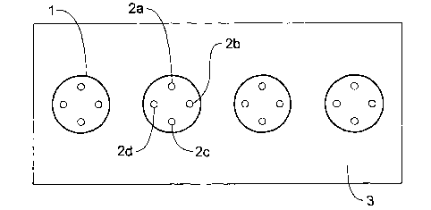
Figure 1 shows an antenna array composed of four DRA elements 1, each of which
is
fitted with four internal probes 2a, 2b, 2c, 2d and mounted on a grounded
substrate 3.
The spacing of the array elements 1 is a half of a wavelength. Antenna pattern
14
CA 02402556 2002-09-11
WO 01/69722 PCT/GBO1/00997
10
steering is achieved using power splitter/combiners (not shown) and cable (not
shown) delays to drive the elements. Element pattern steering is achieved by
switching between probes 2, or by using power splitter/combiners to drive two
probes 2 simultaneously.
Each DRA element 1, when excited in a preferred HEM1 1g mode, which is a
hybrid
electromagnetic resonance mode radiating like a horizontal magnetic dipole,
gives
rise to a vertically polarised radiation pattern with a cosine or figure-of
eight shaped
pattern.
When a broadside (boresight) antenna pattern is formed using one probe 2 in
each
element 1 (in this case, the upper probe 2a in each DRA element 1 of Figure 1
), the
pattern produced is substantially as predicted by theory, as shown in Figure
2.
The array of Figure 1 is also capable of operating in end-fire mode by
switching to
the probe 2b in each DRA element l, which is internally disposed at 90 degrees
to
the probe 2a used for broadside operation. Again, the agreement with theory is
excellent, as can be seen in Figure 3. Switching probes to allow the array to
end-fire
is an important facility as it enables the array to steer through 360 degrees.
When the
opposite internal DRA probes are used to end-fire in the opposite direction, a
pattern
almost identical to Figure 3 is obtained, except with a left-right reverse.
The array factor may be steered by inserting cable delays in the feeds to each
probe 2
in each element 1. Figure 4 shows the result of steering the antenna pattern
by a
nominal 41.5 degrees in a given direction from broadside in azimuth (the aim
was a
steering angle of 45 degrees, but the cables available prevented this being
achieved
exactly). Initially, the probes 2a used to form the broadside pattern were
used - this
represents the usual case for an array when no element steering is available.
Also
shown in Figure 4 are the measured patterns when two probes 2a, 2b are used in
each
DRA element 1 to steer the element pattern to roughly 45 degrees. The increase
in
array gain caused by steering the elements 1 in synchronism with the array
pattern is
clearly apparent. It should also be noted that in the two-probe case, there is
an
additional loss in the power sputters of about 1 dB, so the actual effect is
better than
displayed in Figure 4. It can also be seen that there is a dramatic
improvement in the
antenna pattern in that a large sidelobe at around 140 degrees has been
significantly
reduced. This illustrates a further benefit of element beamsteering.
CA 02402556 2002-09-11
WO 01/69722 PCT/GBO1/00997
The results for steering about =l~ degrees to the other side of broadside are
shown in
Figure 5. It can be seen that the results are almost a 'mirror image' of those
shown in
Figure 4, and that the increase in gain and main sidelobe reduction arising
from
element steering is again achieved.
The benefits of gain recovery by element beam steering are determined by
measuring
the S 12 transmission loss between the terminals of a network analyser being
used to
measure the antenna patterns. These can be summarised as follows:
Pattern Expected Measured
S 12 transmission loss of broadside pattern -X2.1 dB -X2.1 dB
S 12 transmission loss of 45° pattern; single probe -54.8dB -
54.9dB
S12 transmission loss of 4~° pattern, two probes -53.8dB -53.9dB
Normalising these results:
Pattern Expected Measured
Normalised broadside gain (reference) O.OdB O.OdB
Array steered to 45° (0.2 dB cable loss subtracted) -2.SdB -2.6dB
Array & elements to 45° (l.OdB sputter loss subtracted) -O.OdB -
0.6dB
When the array only is steered to 45°. the gain on boresight is
expected to drop by
2.SdB due io the cosine pattern of the elements 1. The measured result is
within
0.1 dB of this result at -2.6dB. Cable losses have been removed from the
reading.
When the elements 1 are also steered to 45°, the gain should
theoretically return to
close to that of broadside. The measured result is within 0.6dB of this value.
the
discrepancy mainly being due to the difference between the actual steering to
41.5°
and the nominal steering to 45°.
In order to test whether the two probes steered pattern is as expected, the
theoretical
two probes computed pattern is compared with the measured two probes pattern
of
Figure 4. The results, plotted in Figure 6, show that the agreement between
measurement and theory remains excellent.
Figure 7 shows a vertically-stacked array of multi-segmented compound DRA
elements 10 each being disposed on a grounded substrate 11 and having a
plurality of
feeds 12 for transferring energy into and from the DRAB 10. As shown in Figure
8.
16
CA 02402556 2002-09-11
WO 01/69722 PCT/GBO1/00997
each multi-segmented compound DRA 10 comprises three generally trapezoidal
dielectric resonators 13, 13', 13" arranged on the grounded substrate 11 in a
generally semi-hexagonal configuration, with adjacent side faces of the
dielectric
resonators 13, 13', 13" being separated from each other by a conductive wall
14. A
conductive backplate 15 is provided behind each DRA 10 as shown best in Figure
8.
Each dielectric resonator 13, 13', 13" includes a monopole feed probe 12, and
the
feed probes 12 may be activated either individually or in combination by way
of
electronic circuitry (not shown) connected thereto so as to generate at least
one
incrementally or continuously steerable beam which may be steered through a
predetermined angle a in azimuth.
When four such DRA elements 10 are disposed as elements of a vertical array as
shown in Figure 7 and activated appropriately by way of the feed probes 12, a
resultant beam can be generated which may be steered in elevation ~ as well as
in
azimuth a. The DRAB 10 are vertically separated by a nominal spacing of 7~,/2,
where
~, is the wavelength of the generated beam. In the present example, no
weighting or
window function has been applied, and therefore sidelobe levels are expected
to be
high. Sidelobes may be improved by increasing the number of DRAB 10 in the
array
and also by applying a weighting/window function. The return loss for each DRA
10
in the present example is better than -20dB.
Referring now to Figure 9, this shows the elevation pattern for the array of
Figures 7
and 8 with only the central dielectric resonator 13' of each DRA 10 being
activated.
The vertical beamwidth is determined by the 4-element array factor and is
around 25°
at the -3dB level. The backlobe 16 is determined to some extent by the size of
the
backplate 15, and in the present example is around -27dB.
The length of the conductive walls 14 separating the dielectric resonators 13,
13',
13" can help to determine the azimuth pattern beamwidth. Short walls 14 which
do
not project significantly beyond the dielectric resonators 13, 13', 13" of the
DRA 10
tend to give element beamwidths of around 90°. Longer walls 14 which
project
further beyond the dielectric resonators 13, 13', 13" can bring this beamwidth
down
to 40°. The array factor beamwidths are almost identical to the element
beamwidths,
as expected.
Figure 10 shows the measured azimuth pattern for the array of Figures 7 and 8
with
the central dielectric resonator 13' of each DRA 10 being activated. DRAs 10
with
17
CA 02402556 2002-09-11
WO 01/69722 PCT/GBO1/00997
short walls 14 projecting only just beyond the dielectric resonators 13, 13',
13" were
used, and the beamwidth is therefore around 90°. The backlobe 17 is of
the same
order as before, that is, around -25dB
Figure 11 shows the measured azimuth pattern for the array of Figures 7 and 8
with
the left-hand dielectric resonators 13 of each DRA 10 being activated. It can
be seen
that the array factor has been steered by around 75°, and that the
backlobe 17 is worse
than in Figure 10. being around -l3dB.
The array of Figures 7 and 8 may be used as a base station antenna for a GSM
mobile
communications network, with beamsteering in both azimuth and elevation. The
elevation pattern is controlled by the array factor of the array, and the
azimuth pattern
by feeding the dielectric resonators 13, 13', 13" in each DRA 10 in various
combinations or individually and also by selecting appropriate lengths for the
conducting walls 14. Such a base station antenna may be engineered to
specifications for a conventional second generation GSM system. The antenna
may
be roughly lOcm wide, 80cm high and Scm deep, and can be operated so as to
generate three independent azimuth beams (which could be combined and steered,
or
used for direction finding), each one of which may have a 10-15°
elevation pattern.
Each beam may be used on a separate frequency within a 160MHz band. By using
appropriate ceramics as a material for the dielectric resonators 13, 13', 13",
low
losses may be achieved.
For full 360° beamsteering in azimuth, an array of four DRAs 20 each
composed of
six trapezoidal dielectric resonators 21 arranged in a hexagonal configuration
and
separated by conductive walls 22 may be used, as shown in Figure 12.
35
18