Note: Descriptions are shown in the official language in which they were submitted.
CA 02402825 2010-04-22
WO 01/7-5984 PCT/USOO/16912
1
Antireflection Coated Refractory Metal Matched Emitters
for Use in Thermophotovoltaic Generators
BACKGROUND OF THE INVENTION
Recently, low bandgap photovoltaic cells such as the
GaSb cell have made it possible to produce practical
thermophotovoltaic (TPV) electric power generators. The low
bandgap cells in these TPV generators convert infrared (IR)
radiation from heated (IR) emitters into electric power. The
IR emitters in these units operate at moderate temperatures
between 900 C and 1400 C. Baseline commercial TPV
generators use gray-body Sic emitters with GaSb cells. The
Sic emitter emits infrared energy at all wavelengths.
However, the GaSb cells convert only infrared photons with
wavelengths less than 1.8 microns to electric power.
Infrared filters are used to reflect some of the non-useful
longer wavelength photons back to the emitter.
Unfortunately, the available filters are far from perfect.
Some non-convertible infrared radiation still passes through
the filters, and some of the reflected photons do not hit the
emitter after reflection by the filter.
It is preferable to replace the gray-body emitter with a
"matched" infrared emitter that emits only convertible
infrared radiation. Mathematically, this perfect "matched"
emitter has an emittance of 1.0 for wavelengths less than 1.8
microns and 0 for longer wavelengths. Several prior art
infrared emitters have been proposed for use in TPV
generators.
The oldest type of IR emitter proposed is the rare earth
oxide selective emitter. Erbia is an example of this type of
emitter. While the emittance at 1.5 microns can be as high
as 0.5, the emittance for erbia falls to 0.1 at 1.4 and 1.6
microns and rises again beyond 3 microns. The result is that
the emitted useful power is small because of the narrow
emittance bandwidth. Furthermore, the spectral efficiency,
CA 02402825 2002-10-03
WO 01/75984 PCT/US00/16912
2
defined as the in-band convertible power divided by the total
emitted power, is low because a lot of power is emitted at
wavelengths beyond 3 microns.
Refractory metal IR emitters, such as tungsten, have
also been described. Those materials are somewhat selective
in that the emittance at 1.5 microns (typically 0.3) is
higher than the emittance at longer wavelengths (0.15 at 3
microns). Unlike the oxide emitters, the emittance stays low
at long wavelengths (0.1 at 6 microns). Unfortunately,
these metal emitters need to run very hot because of the low
in-band emittance. They also produce volatile oxides when
operated in air.
Recently, JX Crystals has described a cobalt doped
spinel "matched" emitter. This "matched" emitter has an
emittance of 0.7 at 1.5 microns with a large bandwidth. This
emitter is selective, because the emittance falls off to 0.25
at 3 microns. Unfortunately, however, like all oxide
emitters, the emittance rises again beyond 6 microns.
There are other disadvantages of the oxide emitters.
Specifically, they are subject to cracking upon extensive
thermal cycling, and they have poor thermal conductivity.
It is desirable to find an improved "matched" emitter
with a high emittance at wavelengths below 1.8 microns and
low emittance for all longer wavelengths. It is very
desirable to find a "matched" emitter coating that may be
applied to the current SiC emitter structures, since SiC is a
proven material with good thermal conductivity and thermal
cycle durability.
SUMMARY OF THE INVENTION
The invention provides a matched emitter which emits
infrared radiation at 1.8 microns and less than 1.8 microns
to match the wavelengths of photons that GaSb cells absorb
and convert to electricity.
In one form, a refractory metal coating such as tungsten
(W) having a thickness of about 4 microns or from about 1-6
CA 02402825 2002-10-03
WO 01/75984 PCT/US00/16912
3
microns is deposited on a durable high temperature substrate
such as SiC. The W coating may be isolated chemically from
the substrate by a refractory oxide coating, such as Hf02,
Ta2051 Zr02 or A1203, so that it does not react with the
substrate. The W coating is coated with a high index
refractory oxide coating of a thickness such that a minimum
reflectivity occurs in the center of the cell convertible
wavelength band. This refractory oxide coating serves as an
anti-reflection (AR) coating. The thickness of the oxide
coating is specifically set to produce an absorption
(emission) peak in the TPV cell conversion wavelength band.
In another embodiment, a refractory inter-metallic
coating such as TaSi2 is deposited on a durable high
temperature substrate such as SiC. The metal silicide
coating may be isolated chemically from the substrate by a
refractory oxide coating, such as Ta205, so that it does not
react with the substrate. In the case that the durable
substrate is SiC, the inter-metallic coating can be a
refractory compound containing a metal such as Ta along with
Si and C. Alternative inter-metallic compounds may include
Pdm(Sii_XCx)or Ptm(Si1_xCx)n. The metal silicide is coated with
a high index refractory oxide coating of a thickness such
that a minimum reflectivity occurs in the center of the cell
convertible wavelength band. This refractory oxide coating
serves as an anti-reflection (AR) coating. The thickness of
the oxide coating is specifically set to produce an
absorption (emission) peak in the TPV cell conversion
wavelength band.
Key elements in this concept are the.reflecting metallic
or inter-metallic coating, the AR coating, and the durable
substrate. In the case of a TPV generator using GaSb cells,
this AR wavelength is about 1.4 microns. A spacer layer may
be provided between the substrate and metallic layers to
prevent interaction of the two.
A typical thickness for the metal silicide is
approximately 4.0 microns, while a typical thickness for the
CA 02402825 2002-10-03
WO 01/75984 PCT/US00/16912
4
refractory oxide AR coatings is approximately 0.14 microns.
Various substrates are possible including but not limited to
SiC, Ta, Nichrome, Kanthal and stainless steel. Various
metal silicides are possible including but not limited to
TaSi2, NbSi2, TiSi2, and VSi2. Various refractory oxides are
possible including, but not limited to, Hf02 , Ta205, A12O3,
TiO2 and Zr02.
Adding Si to the Ta has two beneficial effects. First,
the emittance at 1.5 microns increases from 0.3 to 0.55.
Second, the silicides are more resistant to oxidation.
Adding an AR coating then amplifies on these same two
beneficial effects. The AR coating increases the emittance
again from 0.55 to 0.98 at 1.5 microns, and the refractory
oxide AR coating protects the structure from oxidation.
In another preferred embodiment, another AR coating
includes, but is not limited to, hafnia (Hf02) as the
refractory oxide. Hafnia survives higher temperatures.
Emissivity measurements show excellent spectral selectivity
and no change in emissivity at temperatures up to 1300 C.
This is consistent with the Ultramet data showing that hafnia
has 10-100 times lower vapor pressures and evaporation rates
at 1650 C than either alumina or zirconia. Hafnia also has a
lower thermal expansion coefficient (closer to tungsten) than
alumina or zirconia and a high refractive index of 1.9,
almost as good as zirconia (2.0) and higher than alumina
(1.63). A higher index gives a higher emittance at the
resonant peak.
The AR coated refractory metal "matched" emitters of the
present invention are useable with cells other than the GaSb
cell. They are adaptable to cells that respond out to 2.3
microns by simply shifting the thickness of the AR coating.
They may be used in various environments including air,
vacuum, or various inert atmospheres. They may be used with
various heat sources, including not just hydrocarbon flames
but also nuclear heat sources.
These and further and other objects and features of the
CA 02402825 2002-10-03
WO 01/75984 PCT/US00/16912
invention are apparent in the disclosure, which includes the
above and ongoing written specification, with the claims and
the drawings.
BRIEF DESCRIPTION OF THE DRAWINGS
Figure 1 is a side view of an AR coated refractory metal
matched emitter.
Figure 2 is a graph of the reflection curves for Ta,
TaSi2 and AR coated TaSi2.
Figure 3 is the emittance curve for the refractory metal
silicide matched emitter.
Figure 4 is a graph of the emissive power for the
refractory metal silicide matched emitter and a SiC
(blackbody) emitter.
Figure 5 is a graph of 2nk/A vs wavelength for TaSi2.
Figure 6 is a graph of 2nk/A vs wavelength for several
pure metals.
Figure 7 shows a vertical section through a
thermophotovoltaic generator.
Figure 8 is a graph of the emissivity of hafnia AR
coated tungsten.
DETAILED DESCRIPTION OF THE PREFERRED EMBODIMENTS
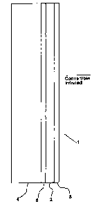
Figure 1 shows the structure of the AR coated refractory
metal "matched" emitter 1 of the present invention. A
refractory metal or metal silicide emitter layer 2, such as W
or TaSi2, is deposited on a durable high temperature
substrate 4, such as SiC. The metal or metal silicide
emitter layer 2 is isolated chemically from the substrate 4
by a refractory oxide 6, such as Hf02, so that the emitter
layer does not react with the substrate. Finally, the metal
or metal silicide 2 is coated with a high index refractory
oxide coating 8 of a thickness such that a minimum
reflectivity occurs in the center of the cell convertible
wavelength band. This refractory oxide coating 8 serves as
an anti-reflection (AR) coating. In the case of a TPV
CA 02402825 2002-10-03
WO 01/75984 PCT/US00/16912
6
generator using GaSb cells, this AR wavelength is about 1.4
microns. A typical thickness for the metal or metal silicide
is approximately 4.0 microns for W or for the TaSi2. A
typical thickness for the refractory oxide coatings is
approximately 0.14 microns. Various substrates 4 are
possible including, but not limited to, SiC, Ta, Nichrome,
Kanthal, and stainless steel. Various refractory metal
emitters 2 are possible, including, but not limited to, W,
Ta, Nb and Mo. Various metal silicides 2 are possible
including, but not limited to, TaSi2, NbSi2, TiSi2, and VSi2.
Various refractory oxides 6 and 8 are possible including, but
not limited to, Hf021 Ta205, A1203, Ti02, and Zr02.
The emitter structure 1 of Figure 1 is effective as a
"matched" emitter for TPV generators (shown in Figure 7).
This may be seen by reference to Tables 1, 2, and 3, and to
Figures 2, 3, and 4. Referring to table 1, the emittances
for SiC, tungsten (W), and cobalt doped spinel at 1.5, 3, and
6 microns are given for reference. Refer now to the
emittances of Ta, TaSi2, and AR coated TaSi2. The emittance
of Ta by itself is similar to that of W. Adding Si to the Ta
has two beneficial effects. First, the emittance at 1.5
microns increases from 0.3 to 0.55. Second, the silicides
are more resistant to oxidation. Adding an AR coating then
amplifies on these same two beneficial effects. The AR
coating increases the emittance again from 0.55 to 0.98 at
1.5 microns, and the refractory oxide AR coating protects the
structure from oxidation.
Figure 2 shows the reflection curves for Ta, TaSi2, and
AR coated TaSi2 as a function of wavelength. Note that while
the reflectivity decreases at 1.5 microns, the reflectivity
at long wavelengths remains high for our refractory metal
silicide "matched" emitter.
Since the absorptance and emittance for metals are
simply 1 minus the reflectivity, Figure 3 shows the emittance
curve for our refractory metal silicide "matched" emitter.
Referring again to Table 1, note that the refractory
CA 02402825 2002-10-03
WO 01/75984 PCT/US00/16912
7
metal silicide "matched" emitter of the present invention has
the highest in-band emittance relative to all of the
available emitters. This means that more electric power is
producible for a given emitter temperature. Also note that
the ratio of in-band emittance to out-of-band emittance for
our AR coated refractory metal "matched" emitter is higher
than for any other emitter. This leads to higher conversion
efficiency.
Figure 4 and Table 2 allow a comparison of a black body
emitter with our refractory metal silicide "matched" emitter.
Figure 4 shows the emissive power as a function of wavelength
for an AR-coated TaSi2 emitter and a blackbody emitter with
both operating at 1400 C. Table 2 gives the calculated
values for the in-band emitted power, the out-of-band emitted
power, and the spectral efficiency for these two emitters.
Note that the in-band power is nearly the same for each,
while the out-of-band power is reduced by a factor of 3 for
the AR-coated TaSi2 emitter. The spectral efficiency is
increased by nearly a factor of 2.
The AR coated refractory silicide "matched" emitters of
the present invention are useable with cells other than the
GaSb cell. They are adaptable to cells that respond out to
2.3 micron wavelengths by simply shifting the thickness of
the AR coating. They may be used in various environments
including air, vacuum, or various inert atmospheres. They
may be used with various heat sources, including not just
hydrocarbon flames but also nuclear heat sources.
The matched emitter concept described here can be
restated in more general terms as follows. Three elements
are required: a durable refractory substrate 4 (Figure 1)
with a refractory metallic (RM) coating 2 (Figure 1) with a
resonant antireflection (AR) coating 8 (Figure 1). In this
three element system, the metallic coating 2 must be
carefully chosen such that the 2nk/A product for the material
drops to 15 or lower at the desired resonant point and then
rapidly rises for longer wavelengths. A spacer layer may be
CA 02402825 2002-10-03
WO 01/75984 PCT/US00/16912
8
provided between the SiC and tungsten layers to prevent
interaction of the two.
Figure 5 shows a plot of 2nk/A vs I for TaSi2, while
Figure 6 shows plots of 2nk/A vs A for various pure metals.
Referring to Figure 6 suggests that pure Ta, W, Nb, or Mo
could be used with an AR coating to create a matched emitter
falling under the present invention. Pure Pd would not work
because the AR coated resonance would be weak.
One of the best specific AR/RM is Hf02 on W. Another
consists of 4 microns of W on SiC followed by an AR coating
of Zr02. Yet another is A1203 AR on W on SiC.
Referring to Figure 7, a thermophotovoltaic (TPV)
generator 15 apparatus includes, in the order of energy flow,
a heat source 3, a matched coated infrared emitter 1, an
optional silica heat shield 7, an infrared filter 9 and a low
bandgap photovoltaic cell receiver 11. The power band of the
emitter 1 is matched with the energy conversion band of the
TPV cells of the receiver 11. The heat source 3 heats the
infrared emitter 1, which in turn emits infrared radiation.
Low bandgap cells of the receiver 11 collect infrared
radiation of a particular wavelength and convert the
collected infrared radiation to electric power.
The refractory oxides include, but is not limited to,
hafnia. Hafnia survives higher temperatures. Figure 8 shows
the emissivity of hafnia (Hf02) AR on tungsten. Emissivity
measurements show excellent spectral selectivity and no
change in emissivity at temperatures up to 1300 C. This is
consistent with the Ultramet data (Table 3) showing hafnia
having 10-100 times lower vapor pressures and evaporation
rates at 1650 C than either alumina or zirconia. Hafnia also
has a lower thermal expansion coefficient (closer to
tungsten) than alumina or zirconia and a high refractive
index of 1.9, almost as good as zirconia (2.0) and higher
than alumina (1.63). A higher index gives a higher emittance
at the resonant peak. A preferred combination includes a
refractory metal coating of tungsten with a hafnia AR
CA 02402825 2002-10-03
WO 01/75984 PCT/US00/16912
9
coating.
While the invention has been described with reference to
specific embodiments, modifications and variations of the
invention may be constructed without departing from the scope
of the invention, which is defined in the following claims.
CA 02402825 2002-10-03
WO 01/75984 PCT/US00/16912
Table 1.
Emittance Values for Various TPV Emitter Materials
Material a at 1.5 m a at 3 Am 0 at 6 um
SiC 0.8 0.85 0.9
W 0.3 0.15 0.1
Co/Spinel 0.7 0.25 0.7
Ta 0.3 0.15 0.1
TaSi2 0.55 0.25 0.15
AR/TaSi2 0.98 0.28 0.15
TABLE 2
Power densities and spectral efficiency at 1400-#C
Material P (0.7 to 1.8 m) P(1.8 to 10) Efficiency
Blackbody 12.2 W/cm2 31.1 W/cm2 0.28
AR/TaSi2 U.S W/cm2 10.7 W/cmZ 0.52
SUBSTITUTE SHEET (RULE 26)
CA 02402825 2002-10-03
WO 01/75984 PCT/US00/16912
11
TABLE 3
REFRACTORY. OXIDES
Ultramet has developed processes for fabricating coatings of the oxides of
hafnium (Hf02).
zirconium (Zr02), tantalum (Ta205), titanium (TiO2), aluminum (Al203), silicon
(Si02) and
yttrium (Y203). These oxides can be applied by CVIJ as a 100% dense, pinhole-
free coating
to a yanety of materials, including [Sfr ctorv metals, corarl3ics and
composites. Used for high
temperature Qx(dation and corrosion resistance (e.g. sulfur, vanadium), these
coatings are
capable of extending either the service life or operating temperature
capability of many
components, including rocket nozzle, piston heads and liners, turbine blades,
and fuel-fired
heat exchanger components.
ThO2 HfO2 Zr02 Y203 A1203 Si02
MELTING TEMPERATURE ("C) 3050 2810 2700 2460 2015 1728
DENSITY (g/cc) 9.86 96B 5.60 5.03 3.98 2.32
THERMAL EXPANSION (ppmi C) 9.5 8.8 7.5 6.8 8.1 0.5
OXIDATION LIMIT ( C) 2700 2500 2500 22007 2015 1680
LIMIT of STABILITY w. ICARBON ( C) 2000 1700 1600 1900
VAPOR PRESSURE (Pa)
(x 10'4) 1650 C 9.41 0.13 10.6 - 133
(x 10-1) @ 1927 C 138 3.93 127 - 50 -
(x 10'3) Q 2200 C 77.0 3.26 78.7 20
EVAPORATION RATE (pm/hr)
(x 10's) a 1650 C 540 6.7 870 - -
1927 C n.74 .0111 0.75 - - -
(Q 2200 C 39 1.4 44 -
CRYSTAL STRUCTURE FCC' FCC' FCC' BCC HCP CT
OXYGEN PERMEABILITY (gtcm-sec)
(x 10'131 @ 1000 C 360 120 9.5
SUBSTITUTE SHEET (RULE 26)