Note: Descriptions are shown in the official language in which they were submitted.
CA 02403754 2002-09-18
WO 01/71514 PCT/USO1/08926
TITLE OF THE INVENTION
A Communication Interface System, Method and Apparatus
BACKGROUND
Field Of The Invention.
The invention relates to a communication interface system, method and
apparatus and, more particularly, to a universal integrated module for
interfacing a
control module to other modules.
Related Information.
In the past, interfaces have been introduced that interface a control module
to
other modules. However, there has been no universal interface for the
interfacing a
plurality of communications protocol as particularly contemplated by the
present
invention.
BRIEF DESCRIPTION OF THE DRAWINGS
Fig. 1 is a table;
Figs. 2a and b are timing diagrams;
Fig. 3 is a table;
Fig. 4 is a timing diagram;
Fig. 5 is a timing diagram;
Fig. 6 is a table;
Fig. 7 is a timing diagram;
Fig. 8 is a timing diagram;
Fig. 9 is a timing diagram;
Fig. 10 is a timing diagram;
Fig. 11 is a timing diagram;
Fig. 12 is a timing diagram;
Fig. 13 is a timing diagram;
1
CA 02403754 2002-09-18
WO 01/71514 PCT/USO1/08926
Fig. 14 is a timing diagram; and
Figs. 15a and 15b are block diagrams.
DETAILED DESCRIPTION OF THE PREFRRED EMBODIMENT
The interface of the present invention provides serial communication to
expansion modules (EM). A CPU of the interface controls all communications to
and
from the EM's and will be referred to as the "Master Function". The Expansion
Module will include an ASIC to achieve this serial communication protocol and
will be
referred to as the "Slave Function" or "Slave ASIC".
The I/O Expansion bus signals as viewed by the Expansion Module are
described in the following table. The connection from the PLC to the EM and
from
EM to EM will be 1 to 1 using a 10 pin header type connection. Refer to Figure
1 for
Expansion I/O Bus connector pin assignments.
The following diagrams in Figures 2a - 2b illustrate an Expansion Bus Read
cycle and Write cycle sequences. A bus transaction will be initiated by short
active
low pulse on XA OD signal. In Fig. 2a:
MA[2:0] - Module Address that CPU is addressing
W - Transaction Type requested by CPU, Read/Write Bit
(1=>Write, 0=>Read)
RA[3:0] - Register Address that CPU is addressing
CP[1:0] - Control Register Parity Bits generated
by CPU
W[7:0] - Data written to Expansion Module
by CPU
DP[1:0] - Data parity generated by CPU
Ack[1:0] - Acknowledge bits returned to CPU by the Slave
- A1 : 0 indicates a successful write cycle (no parity
errors);
1 indicates an invalid write transaction, data parity error
encountered
- AO : defaults to a 1
2
CA 02403754 2002-09-18
WO 01/71514 PCT/USO1/08926
In Fig. 2b:
MA[2:0] - Module Address that CPU is addressing
W - Transaction Type requested by CPU, Read/Write
Bit
(1=>Write, 0=>Read)
RA[3:0] - Register Address that CPU is addressing
CP[1:0] - Control Parity Bits generated by CPU
R[7:0] - Data written to CPU from Expansion Module
DP[1:0] - Data parity generated by Expansion Module
Each EM implements an electrical interface to the expansion I/O bus
consisting of termination circuits and bus driver circuits. This will allow
the addition
of +5V power to be introduced anywhere in the daisy chained I/O bus and
provides
some protection of the SLAVE ASIC I/O. Given that EMD signal is a bi-
directional
signal, control circuitry will be provided on the bus driver circuits to avoid
bus
contention errors. Three control signals (MSTR_IN, MY SLAVE OUT, and '
NEXT SLAVE OUT) are used to enable/disable the EMD bus driver circuits. For
details of the termination circuitry refer to Figure 3. Figure 3 describes EMD
bus
driver circuit configuration for three expansion modules.
A bus driver circuit is provided which has an active low enable line. The
Slave
ASIC generates 3 control signals to properly enable/disable the bus drivers.
Control
signal MSTR_IN enables bus driver circuits A and B. This allows the EMD signal
to
be input into the expansion module ASIC and to be input into the next
expansion
module ASIC down stream. MSTR IN becomes active when XAS is detected and
becomes inactive prior to any response from an EM. The signals MY SLAVE OUT
and NEXT SLAVE OUT control EMD responses from the EM's according to the
EM's physical address position. For example, MY SLAVE OUT controls the EMD
signal as an output of the EM that was addressed by the CPU. The signal
NEXT SLAVE OUT passes the EMD response through the EM if the EM
addressed by the CPU has a higher address or is downstream from that EM.
Neither MY SLAVE OUT or NEXT SLAVE OUT are asserted when the CPU
3
CA 02403754 2002-09-18
WO 01/71514 PCT/USO1/08926
addresses an EM with a lesser address. All three control signals immediately
become inactive on the occurrence of XOD.
In one particular embodiment of the invention, the initial Slave design may be
developed in a 128 Macrocell CPLD using VHDL as a design instrument. The CPLD
design is migrated into an ASIC design. The ASIC is designed to have 44 total
pins
with 36 usable pins for I/O and 8 pins for power and ground. The operating
frequency of the SLAVE ASIC may be 4.125 MHz maximum, which is well within the
ASIC capability. The following table defines the required inputs and outputs
of the
Slave ASIC. Refer to Figure 4 (SLAVE ASIC Suppliers Specification) for details
of
the ASIC.
The I/O described above accommodates all Expansion Module I/O
configurations. That is, the invention is a universal interface. This is
accomplished
by implementing two modes of operation within the ASIC. The differences in
ASIC
operation is the implementation of EXTO and EXT1 data ports.
The slave ASIC has two modes of operation to accommodate all Expansion
Module I/O configurations. In Mode 0, the EXTO bus is an 8 bit input register
and
EXT1 bus will be an 8 bit, active low, output register. EXTO data bus and EXT1
data
bus interfaces directly to the Expansion Module digital I/O. Mode 0 is used
for
Expansion Modules of 81N / 80UT or less. In Mode 1, EXTO bus is used as an 8
bit,
active high, bi-directional data bus and EXT1 bus is used as 8 bits of address
and
control. External registers and decode circuitry are required for Mode 1
operation.
Mode 1 is used when the Expansion Module I/O configuration is greater than 81N
/
80UT or for an intelligent module. The ID REG is decoded by each EM at power
up
to determine its mode of operation. The ID_REG is also be read by the CPU to
determine the Expansion Module type.
The polarity of EXTO data port is "active high" for both Mode 0 and 1. EXT1
data port is "active low" while in mode 0 operation and in mode 1 the control
lines is
"active low" and the address lines is "active high."
4
CA 02403754 2002-09-18
WO 01/71514 PCT/USO1/08926
In operation, the Slave ASIC implements a state machine architecture to
provide proper communication and control. At initial power up the CPU issues
an
active XOD signal. Detection of XOD places the state machine into its home
state
and the EXT1 data port is cleared if in mode 0 or the external output
registers is
cleared if in mode 1. Also at initial power up, the Slave ASIC determines its
Module
Address (MA IN), Mode of operation (Mode 0 or 1) and propagates the next
Module
Address (MA OUT) by incrementing its Module Address by 1. Once XOD is
released, the Slave ASIC state machine continuously monitors the XAS signal
from
its home state. A bus transaction is initiated when XAS becomes active and
transitions to state 0 on the first rising edge of EMCO clock. At state 0 the
state
machine is placed into a known state and propagates to state 1 on the next
rising
edge of EMCO clock. If at any time the XOD signal becomes active, then the
EXT1
data port is asynchronously reset and the state machine returns to its home
state. If
in mode 1 operation, the external output registers is asynchronously cleared
and the
state machine returns to its home state. The next occurrence of XAS
synchronously
places the state machine into a known state.
Fig. 5 illustgrates a Mode 0 Write Transaction. As shown in Fig. 5, once a
valid XAS is detected the Slave ASIC propagates to state 0 of the control
state
machine on the first rising edge of EMCO clock. At state 0, the MSTR IN signal
is
asserted and the EMD signal is enabled as an input to the Slave ASIC. The
control
state machine begins to shift in the control register data beginning on the
rising edge
of EMCO clock 1 (state 1 ) and ending on the rising edge of EMCO clock 10
(state 10).
At state 4 (EMCO clock 4) the Slave ASIC determines if the Module Address (MA)
shifted in from the CPU equals the Module Address (MA IN) propagated in at
power
up and if true "My_addr" is asserted. In the case that the addresses do not
match,
My_addr is not asserted, and the state machine continues through the remaining
states to account for proper EMD bus driver control and control register
parity
checks. At State 10 the Slave ASIC determine the type of transaction to occur
and
enters either the write state machine or read state machine on the next EMCO
clock.
During a write transaction the Slave ASIC shifts in Write data beginning at
state 11
(EMCO clock 11) and ending at state 20 (EMCO 20). Also, during state 11 the
control
register parity is checked and in the event an error is detected on the
control register
the write state machine returns to an idle state and the control state machine
returns
CA 02403754 2002-09-18
WO 01/71514 PCT/USO1/08926
to its home state on the next EMCO clock. EXT1 data port is not disturbed and
the
MSTR_IN bus control signal becomes nactive. If no control register parity
error is
detected then the write data is shifted in accordingly. At state 20 the
MSTR_IN bus
control signal is released and at state 21 the state machine preparesthe EMD
bus
control signals for a response back to the CPU. If "My_addr" is valid then
MY SLAVE OUT bus control signal is asserted. If "My_addr" is not valid then
the
NEXT SLAVE OUT bus control signal is asserted only if the CPU has addressed a
module of a greater address. At state 22 the Slave ASIC checks parity on the
write
data. When a write data parity error is detectedhe Slave ASIC returnsan
invalid (11)
Acknowledge to the CPU and does not present new data to EXT1 data port. If no
parity error is detected, then the Slave ASIC returns a valid (01 )
Acknowledge to the
CPU, decodes the register address (RA) and enables new data onto the EXT1 data
port if register address 'C' (hex) has been decoded. If any other register is
decoded
the state machine will returns a valid Acknowledge to the CPU, but does not
present
new data to the EXT1 data port. This is only true while in mode 0 operation.
On the
rising edge of EMCO clock 24 the write state machine returns to an idle state
and the
control state machine returns to its home state.
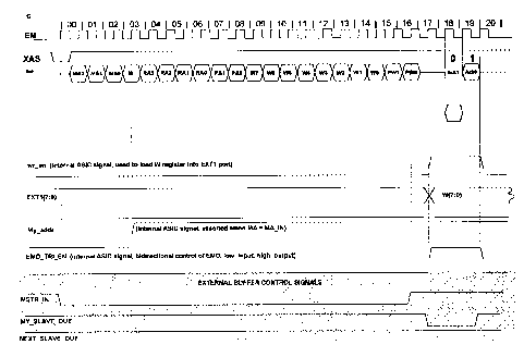
Figure 6 illustrates a mode 0 read transaction with the CPU addressing RA
8(hex). The control state machine operates the same as the previous write bus
transaction, except at state 10 it now enters the read state machine. At state
11 the
read machine releases the EMD bus control signal MSTR_IN, select the EMD
(EMD TRI_EN) bi-directional port as an output, and checks the control register
parity. If a parity error occurs the read state machine returns to an idle
state and the
control state machine returns to a home state on the next rising edge of EMCO
clock.
If no error was detected then the read state machine propagates to state 12 on
the
next rising edge of EMCO clock. At state 12 the state machine prepares the EMD
bus control signals for a response back to the CPU by asserting bus control
signal
MY SLAVE OUT. Also at state 12 the register address (RA) is decoded to
determine the data source. If RA decodes to 0 then the ID BUF data is enabled,
if
RA decodes to 8 then EXTO data bus is enabled, and if any other address is
decoded then the hex value FF is enabled. On the falling edge of EMCO 12 the
"R"
register is loaded with the appropriate data either from the EXTO data bus,
the
ID BUF, or the default value of FF. For the case in Figure 2 the EXTO data is
loaded
6
CA 02403754 2002-09-18
WO 01/71514 PCT/USO1/08926
into the "R" register. On the next rising edge of EMCO clock (state 13) the
read state
machine shifts the read data bit 7 onto the EMD line and the last read bit 0
is shifted
in on the rising edge of EMCO clock 20 (state 20). The Slave ASIC generates 2
parity bits, PR1 and PRO, on the 8 bits of read data and shift this data onto
the EMD
line at states 21 and 22. At state 23 all EMD bus control signals are
released, the
read machine returns to an idle state and the control machine returns to its
home
state.
Mode 1 Operation will now be discussed with reference to Fig. 7.
The EXT1 bus will be used as a control port in ASIC Mode 1. The table in Fig.
7
describes each bit for EXT1 data port when in ASIC Mode 1.
In a Mode 1 Write Transaction, the control register state machine and the
write state machine function the same as in mode 0, however the external port
usage and the available registers differs from mode 0. In mode 1, EXT1 data
port is
used as a control port for external decode circuitry and EXTO data port is a
bi-
directional data port. Write data is enabled onto EXTO data port on the rising
edge of
EMCO clock 21 and is valid for 3 clock periods. The Register Address (RA[3:0])
is
clock'd onto EXT1 data port on the falling edge of EMCO clocks 5, 6, 7, & 8
respectively. All 16 register addresses is available for external decode. The
WRSTRB is asserted on the falling edge of ECMO clock 22 and is cleared on the
falling edge of EMCO clock 23. The signal Busy is asserted on the falling edge
of
EMCO clock 16 and is cleared on the falling edge of EMCO clock 24. If a parity
error
is detected on the WRITE byte, then both the ASIC registers and the external
registers retain their last received value. Refer to the figures 8 and 9 for
detailed
timing information for a time exploded view of Mode 1, Write Transaction
Timing.
CA 02403754 2002-09-19
In a Mode 1 Read l'ransactian, the control register state machine and the
read :late machine function the same as in mode 0, however external port usage
and the available registers differ from mode 0. In mode 1, EXT.1 data port is
used as
a con:rol pert for external decode circuitry and EXTO data port is a bi-
directional data
port. Also, the CPU can access ali 16 registers in Mode 1 with register 0
stilt the ID
register. Refer to Figures 10 and 11 for timing details of the control port
EXT1 and
the d;~ta port EXTO.. Figs. 10 and 11 illustrate Mode 1, Read Transaction
Timing.
ID REagister Definitlan:
The ID Register is addressed from Register Address (RA) 00 hex. The Slave
ASICr fills bit ? with a 0 and the remaining 7 bits are hardwired according to
the
Module type. According to the ID Register definition, the Slave ASIC operates
in
ASIC Mode 0 only for 1D Register values of 01, 04, and 05 hex. All other ID
Register
values operate in Mode 1.
Figs. 12-14 contains mode 1 Read and Write Bus transactions that display
vari«us parity errors_ The figures illustrate the Bus operationlresponse under
these
conditions. Mode 0 bus transactians respond to these errors in the same
rr~anner_
Fig. 12 illustrates Mode 1, Control Register Parity Error during a Write
Transaction.
Fig. 13 iltustrates Mode 1, Write Register Parity Error during a Write
Transaction.
Fig. 14 illustrates MODE 1, Control Register Parity Error During a READ
Transaction.
Figs. 15a and 15b illustrate the two modes in block diagram form. As shown
in F=ig. 15a, the slave ASIC is in mode 1. In this state, a first bus line is
dedicated as
an output and the second bus provides control lines far sending control
signals to the
attached modules. In Fig. 15b, the same slave ASIC is switched into mode 0. In
this
state, the first bus remains a bused output. The second bus, however, is
switched to
a bused input. Thereby, the invention realizes the universal interface for a
plurality
of modes as contemplated in the description of the modes above.
While the present invention is described with reference to particular
Embodiments, it wilt be appreciated that the invention is not so limited to a
specific
Em p f a n g s AMENDED SHEET
CA 02403754 2002-09-18
WO 01/71514 PCT/USO1/08926
embodiment, but may encompass all modifications and permutations that are
within
the scope of the invention.