Some of the information on this Web page has been provided by external sources. The Government of Canada is not responsible for the accuracy, reliability or currency of the information supplied by external sources. Users wishing to rely upon this information should consult directly with the source of the information. Content provided by external sources is not subject to official languages, privacy and accessibility requirements.
Any discrepancies in the text and image of the Claims and Abstract are due to differing posting times. Text of the Claims and Abstract are posted:
| (12) Patent: | (11) CA 2403864 |
|---|---|
| (54) English Title: | METHOD FOR MAKING AN ELECTROCONDUCTIVE JOINT |
| (54) French Title: | PROCEDE DE FABRICATION D'UN JOINT ELECTROCONDUCTEUR |
| Status: | Expired and beyond the Period of Reversal |
| (51) International Patent Classification (IPC): |
|
|---|---|
| (72) Inventors : |
|
| (73) Owners : |
|
| (71) Applicants : |
|
| (74) Agent: | NORTON ROSE FULBRIGHT CANADA LLP/S.E.N.C.R.L., S.R.L. |
| (74) Associate agent: | |
| (45) Issued: | 2010-06-08 |
| (86) PCT Filing Date: | 2001-03-21 |
| (87) Open to Public Inspection: | 2001-09-27 |
| Examination requested: | 2006-02-28 |
| Availability of licence: | N/A |
| Dedicated to the Public: | N/A |
| (25) Language of filing: | English |
| Patent Cooperation Treaty (PCT): | Yes |
|---|---|
| (86) PCT Filing Number: | PCT/FI2001/000281 |
| (87) International Publication Number: | FI2001000281 |
| (85) National Entry: | 2002-09-20 |
| (30) Application Priority Data: | ||||||
|---|---|---|---|---|---|---|
|
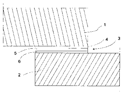
A method for creating an electroconductive joint in connection with conductor
rails made of copper or copper alloy, in which method in between the conductor
rail elements to be joined, there is applied soldering/brazing agent,
whereafter at least the junction area is heated, so that a joint is created.
According to the method, the employed soldering/brazing agent is a layered
soldering/brazing agent foil (3) comprising surface layers (4, 6) and an
intermediate layer (5) therebetween, and the junction area is thermally
treated, so that a diffusion joint is created.
Procédé de fabrication d'un joint électroconducteur en connexion avec des rails conducteurs constitués de cuivre ou d'alliages de cuivre. Selon ledit procédé, un métal d'apport de soudage/brasage est appliqué entre les éléments de rail conducteur à joindre, après quoi au moins la zone de jonction est chauffée, si bien qu'un joint est ainsi créé. Selon la présente invention, le métal d'apport de soudage/brasage se présente sous forme de feuille (3) à plusieurs couches comportant des couches de surface (4, 6) et une couche intermédiaire (5) située entre les deux couches de surface. La zone de jonction est soumise à un traitement thermique, si bien qu'un joint de diffusion est ainsi créé.
Note: Claims are shown in the official language in which they were submitted.
Note: Descriptions are shown in the official language in which they were submitted.
2024-08-01:As part of the Next Generation Patents (NGP) transition, the Canadian Patents Database (CPD) now contains a more detailed Event History, which replicates the Event Log of our new back-office solution.
Please note that "Inactive:" events refers to events no longer in use in our new back-office solution.
For a clearer understanding of the status of the application/patent presented on this page, the site Disclaimer , as well as the definitions for Patent , Event History , Maintenance Fee and Payment History should be consulted.
| Description | Date |
|---|---|
| Time Limit for Reversal Expired | 2012-03-21 |
| Letter Sent | 2011-03-21 |
| Grant by Issuance | 2010-06-08 |
| Inactive: Cover page published | 2010-06-07 |
| Inactive: Final fee received | 2010-03-18 |
| Pre-grant | 2010-03-18 |
| Letter Sent | 2010-02-21 |
| Inactive: Single transfer | 2010-01-19 |
| Notice of Allowance is Issued | 2009-11-24 |
| Letter Sent | 2009-11-24 |
| Notice of Allowance is Issued | 2009-11-24 |
| Inactive: Approved for allowance (AFA) | 2009-11-19 |
| Amendment Received - Voluntary Amendment | 2009-08-20 |
| Inactive: S.30(2) Rules - Examiner requisition | 2009-03-04 |
| Amendment Received - Voluntary Amendment | 2008-12-17 |
| Inactive: S.30(2) Rules - Examiner requisition | 2008-07-15 |
| Letter Sent | 2006-03-17 |
| Inactive: IPC from MCD | 2006-03-12 |
| Inactive: IPC from MCD | 2006-03-12 |
| Inactive: IPC from MCD | 2006-03-12 |
| Inactive: IPC from MCD | 2006-03-12 |
| Request for Examination Received | 2006-02-28 |
| Request for Examination Requirements Determined Compliant | 2006-02-28 |
| All Requirements for Examination Determined Compliant | 2006-02-28 |
| Amendment Received - Voluntary Amendment | 2006-02-28 |
| Letter Sent | 2003-01-21 |
| Inactive: Cover page published | 2003-01-17 |
| Inactive: Notice - National entry - No RFE | 2003-01-15 |
| Inactive: Single transfer | 2002-11-12 |
| Application Received - PCT | 2002-10-29 |
| National Entry Requirements Determined Compliant | 2002-09-20 |
| Application Published (Open to Public Inspection) | 2001-09-27 |
There is no abandonment history.
The last payment was received on 2010-02-23
Note : If the full payment has not been received on or before the date indicated, a further fee may be required which may be one of the following
Patent fees are adjusted on the 1st of January every year. The amounts above are the current amounts if received by December 31 of the current year.
Please refer to the CIPO
Patent Fees
web page to see all current fee amounts.
| Fee Type | Anniversary Year | Due Date | Paid Date |
|---|---|---|---|
| Basic national fee - standard | 2002-09-20 | ||
| MF (application, 2nd anniv.) - standard | 02 | 2003-03-21 | 2002-09-20 |
| Registration of a document | 2002-11-12 | ||
| MF (application, 3rd anniv.) - standard | 03 | 2004-03-22 | 2004-02-10 |
| MF (application, 4th anniv.) - standard | 04 | 2005-03-21 | 2005-02-17 |
| MF (application, 5th anniv.) - standard | 05 | 2006-03-21 | 2006-02-21 |
| Request for examination - standard | 2006-02-28 | ||
| MF (application, 6th anniv.) - standard | 06 | 2007-03-21 | 2007-02-16 |
| MF (application, 7th anniv.) - standard | 07 | 2008-03-21 | 2008-02-28 |
| MF (application, 8th anniv.) - standard | 08 | 2009-03-23 | 2009-03-13 |
| Registration of a document | 2010-01-19 | ||
| MF (application, 9th anniv.) - standard | 09 | 2010-03-22 | 2010-02-23 |
| Final fee - standard | 2010-03-18 |
Note: Records showing the ownership history in alphabetical order.
| Current Owners on Record |
|---|
| OUTOTEC OYJ |
| Past Owners on Record |
|---|
| VEIKKO POLVI |

