Note: Descriptions are shown in the official language in which they were submitted.
CA 02404811 2002-09-27
t .
DESCRIPTION
FLAT DISCHARGE DISPLAY DEVICE
TECHNICAL FIELD
The present invention relates to a planar discharge
display device in which glass frits are coated not only around
a front glass substrate and a rear glass substrate but also on
the spaces between a plurality of unit discharge display portions
and the adjacent unit discharge display portions of a front glass
substrate and then the front glass substrate and a rear glass
substrate are joined by the glass frits to thereby form a flat
tube-assembly.
BACKGROUND ART
In a general structure of a planar discharge display
device called a PDP (Plasma Display Panel) according to the prior
art, a front glass substrate and a rear glass substrate in which
respective members such as electrodes, ribs and fluorescent
substances are provided are opposed to each other and are brought
in contact with each other such that respective members are
assembled together in a predetermined relationship and the
surrounding portions of the two glass substrates are j oined by
glass frits and sealed in vacuum, thereby forming a planar
discharge display device having a flat tube-assembly.
In this case, in the inside of the flat tube-assembly,
the members formed on the two glass substrates are only contacted
with each other but are not joined together. Then, in the planar
discharge display device having such structure, since the two
1
CA 02404811 2002-09-27
glass substrates are j oined at the glass frit portions of the
surrounding portions , a frit coating width of a certain width,
i . a . , so-called margin is required in order to maintain adhesive
strength. A width of this margin generally ranges approximately
several millimeters to 10 millimeters.
Accordingly, the assignee of the present application
has previously proposed a planar discharge display device in
which glass frits are coated not only on the surrounding portions
of the front glass substrates and the rear glass substrates but
also on spaces between unit discharge display portions of a
plurality of unit discharge display portions [one cell or a
plurality of discharge cells (pixel of single color or pixel
comprising a set of three primary colors)] of a front glass
substrate and a rear glass substrate and adjacent discharge
display portions and the front glass substrate and the rear glass
substrate are joined by such glass frits to thereby form a flat
tube-assembly [see (Japanese patent application No. 7-317626)
and (Japanese laid-open patent application No. 9-129143)]. In
the planar discharge display device of this case, a plurality
of unit discharge display portions are provided in an XY matrix
fashion.
In such planar discharge display device, since the
glass frits are coated on not only the surrounding portions of
the front glass substrate and the rear glass substrate but also
on the spaces between a plurality of unit discharge display
portions and the adj acent to j oin the front glass substrate and
2
' CA 02404811 2002-09-27
the rear glass substrate, distortions and stress of the front
glass substrate and the rear glass substrate are dispersed and
burden imposed upon the frits coated on the surrounding portions
of the front glass substrate and the rear glass substrate can
be reduced considerably. Therefore, the widths of the glass frits
coated on the surrounding portions of the front glass substrate
and the rear glass substrate can be minimized.
However, in such planar discharge display device,
depending upon the thickness of the glass frit coated on the
spaces between the respective unit discharge display portions
of a plurality of unit discharge display portions and the adj acent
unit discharge display portions of the front glass substrates
and the rear glass substrates, a gap is produced between the
front glass substrate and the rear glass substrate so that
discharge occurs unintentionally to cause crosstalk to occur.
Moreover, because the thickness of the glass frit is not uniform,
there arises a problem such as bonding failure.
In view of the aforesaid aspect, according to the
present invention, there is provided a planar discharge display
device in which glass frit is coated on the surrounding portions
of the rear glass substrate and the front glass substrate, glass
frit is also coated on the spaces between a plurality of unit
discharge display portions and the adjacent unit discharge
display portions of the rear glass substrate and the front glass
substrate and then the rear glass substrate and the front glass
substrate are joined with pressure under the condition in which
3
' CA 02404811 2002-09-27
glass frit is being heated to thereby form a vacuum flat
tube-assembly into which discharge gas is filled. In this planar
discharge display device, there can be removed risks in which
crosstalk is caused by erroneous discharge and in which bonding
failure is caused due to uneven thickness of glass frits.
DISCLOSURE OF INVENTION
According to the first invention, there is provided
a planar discharge display device including projection-like
structure members provided in spaces between a plurality of unit
discharge display portions and the adjacent unit discharge
display portions of one and the other of a rear glass substrate
and a front glass substrate, recesses engaged with the
projection-like structure members and glass frits coated on the
surrounding portions of the rear glass substrate and the front
glass substrate and coated between the proj ection-like structure
members and the recesses which are respectively engaged with
the projection-like structure members, in which the rear glass
substrate and the front glass substrates are j oined with pressure
under the condition in which glass frit is being heated to thereby
form a vacuum flat tube-assembly into which discharge gas is
filled.
According to the second invention, there is provided
a planar discharge display device including recesses formed on
spaces between a plurality of unit discharge display portions
and unit discharge display portions adj oining to the respective
unit discharge display portions of a front glass substrate and
4
CA 02404811 2002-09-27
portions coated with fluorescent substances by sandblast or
chemical etching, projection-like structure members
respectively engaged with the recesses formed on the spaces
between a plurality of unit discharge display portions and the
unit discharge display portions adj oining to the respective unit
discharge display portions and which are also engaged with the
recesses formed on the spaces between a plurality of unit
discharge display portions and the unit discharge display
portions adjoining to the respective unit discharge display
portions, fluorescent substances coated on the front glass
substrate at its recesses coated with fluorescent substances
and glass frits provided on the surrounding portions of the rear
glass substrate and the front glass substrate and between the
recesses and the respective projection-like structure members
engaged with the respective recesses, in which the rear glass
substrate and the front glass substrate are j oined with pressure
under the condition in which glass frit is being heated to thereby
form a vacuum flat tube-assembly into which discharge gas is
filled.
BRIEF DESCRIPTION OF DRAWINGS
FIG. 1 is a perspective view showing a planar display
device according to an embodiment of the present invention in
an exploded fashion. FIG. 2 is a fragmentary cross-sectional
view showing a planar display device according to an embodiment
of the present invention. FIG. 3 is a fragmentary cross-sectional
view showing a planar display device according to another
CA 02404811 2002-09-27
embodiment of the present invention.
BEST MODE FOR CARRYING OUT THE INVENTION
First , a structure of a planar discharge display device
according to an embodiment of the present invention will be
described with reference to FIGS . 1 and 2 . FIG. 1 is an exploded
perspective view of a planar discharge display device, and FIG.
2 is a fragmentary cross-sectional view thereof.
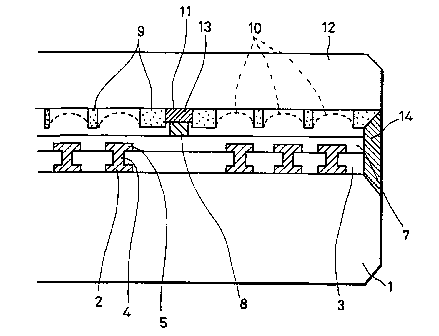
Proj ection-like structure members 8 formed on a rear
glass substrate 1 and recesses 11 formed on a front glass substrate
12 characterize a planar discharge display device according to
this embodiment. Alternatively, the projection-like structure
members 8 may be formed on the front glass substrate 12 and the
recesses 11 may be formed on the front glass substrate 1.
When the rear glass substrate 1 and the front glass
substrate 12 are assembled, the proj ection-like structure member
8 and the recess 11 are opposed to each other. As shown in FIG.
2, the projection-like structure member 8 and the recess 11 are
shaped so as to be engaged with each other and joined by glass
frit 13 interposed between the proj ection-like structure member
8 and the recess 11.
To hold a flat tube-assembly comprising the rear glass
substrate 1 and the front glass substrate 12 at the vacuum state,
peripheral portions of the rear glass substrate 1 and the front
glass substrate 12 are coated with another end-sealing glass
frit 14.
Next, an overall structure of this planar discharge
6
CA 02404811 2002-09-27
display device will be described with reference to FIGS . 1 and
2. Although discharge electrodes 2, 5 and 6 which are formed
on the rear glass substrate 1 as shown in FIG. 1 are not directly
related to the glass joint structure which is one of the
characteristics of the present invention and are only examples
for use in explaining the present invention, these discharge
electrodes will be described below.
First, a plurality of first electrodes 2 is formed
on the rear glass substrate 1 in parallel to each other by a
suitable method such as screen-printing. Next, an insulating
layer 3 is formed so as to cover a plurality of first electrodes
2.
The insulating layer 3 has through-holes 4 defined
thereon. The through-holes 4 can be easily formed by a screen
mask with a through-hole pattern at the same time the insulating
layer 3 is formed with the screen mask by screen printing or
the like.
A plurality of second electrodes 6 are formed on the
insulating layer 3 in parallel to each other in such that they
may cross a plurality of first electrodes 2, and a plurality
of slit-like electrodes 5 are formed on the insulating layer
through the through-holes 4 in such a manner that they may be
connected to a plurality of electrodes 2, respectively. In this
manner, the first and second electrodes 2 and 6 form an XY matrix,
which may cross each other through the insulating layer 3. In
actual practice, discharge is generated between a selected
7
CA 02404811 2002-09-27
electrode of a plurality of second electrodes 6 and a selected
electrode of a plurality of slit-like electrodes 5.
A plurality of second electrodes 6 are covered with
a dielectric layer 7 and the dielectric layer 7 is covered with
a protective layer (not shown) such as oxide magnesium and thereby
an AC discharge electrodesareformed.Alternatively,a plurality
of second electrodes may form DC electrodes without the
dielectric layer 7.
After the electrodes and the like needed by discharge
to display images have been formed as described above, as shown
in FIGS . 1 and 2 , a plurality of proj ection-like structure members
8 are formed on the dielectric layer 7. The projection-like
structure members 8 can be easily formed at high accuracy by
effectinglaminationscreen-printing on asuitable materialsuch
as low-melting glass.
The proj ection-like structure members 8 may be shaped
freely so long as they can be fitted into the recesses 11 formed
on the front glass substrate 12 , which will be described later
on, e.g., they may be shaped like plates, hemispheres and so
on. Stated otherwise, the recesses I1 may be shaped in such a
manner that they can be fitted into the proj ection-like structure
members 8. After the projection-like structure members 8 have
been formed, the joint frit 13 is coated on the upper surface
of the projection-like structure members or the body of the
proj ection-like structure members 8 and temporarily dried. The
joint glass frit may be the same material as that of end-sealing
8
CA 02404811 2002-09-27
glass frit 14 which is used to end-seal the peripheral portions
of the rear glass substrate and the front glass substrate in
the vacuum state or may be a different material depending upon
the manufacturing process.
A proper height of the projection-like structure
member 8 may fall within a range of from approximately 0.1 mm
to approximately 0.2 mm when a thickness of rib patterns 9 on
the front glass substrate 12 and a thickness of the j oint glass
frit 14 are considered as shown in FIG. 3.
Next, as shown in FIG. 2, the front glass substrate
12 has formed thereon a set of three recesses for use as a set
of three pixels 10 which are respectively coated with red, blue
and green fluorescent substances, and red, blue and green
fluorescent substances may be coated on the recesses for use
as a set of three pixels 10 and thereby a set of pixels 10 comprising
the red, blue and green fluorescent substances are formed.
The unit discharge display portion is composed of one
or a plurality of discharge cells (pixel of single color or pixel
formed of a set of three primary colors).
The recess 11 engaged with the projection-like
structure member 8 of the rear glass substrate 1 side is formed
on the portion between the pixel 10 and the adj acent pixel . These
pixel 10 and recess 11 are formed by a method similar to that,
which is used to form a rib (rib) in an ordinary PDP . For example,
when a general rib pattern 9 is formed, low-melting glass may
be laminated with patterns by printing or rib members having
9
CA 02404811 2002-09-27
a proper thickness , a . g. , approximately ranging from 0 . 1 mm to
0 . 2 mm may be laminated on the whole and the laminated rib members
may be treated with patterns by a suitable method such as sandblast .
The ordinary rib pattern 9 is made of a black material in order
to improve contrast. Fluorescent substances are coated on the
recess of the pixel 10 thus formed by a suitable method such
as screen-printing and bonding glass frit 13 is coated on the
recess 11.
A plurality of projection-like structure members 8
and a plurality of recesses 11 which had been formed on the rear
glass substrate 1 and the front glass substrate 12 in which
respective members are formed are respectively engaged with each
other through the glass frits 13 . Further, the end-sealing glass
frits 14 are coated on the surrounding portions of the rear glass
substrate 1 and the front glass substrate 12. Thereafter, when
the whole of the resultant product is heated at about 450°C,
the glass frits 13 and 14 are melted to bond the two glass
substrates 1 , 12 and an air-tight flat tube-assembly which is
vacuum tolerable in the inside can be constructed of the rear
glass substrate 1 and the front glass substrate 12.
Then, in the later process, after the inside of the
flat tube-assembly has been made vacuum temporarily, gas
necessary for discharging, a . g. , a mixed gas such as neon gas ,
argon gas or xenon gas is filled into the flat tube-assembly
and thereby the planar discharge display device is formed.
CA 02404811 2002-09-27
Next, a structure of a planar discharge display device
according to another embodiment of the present invention will
be described with reference to a fragmentary cross-sectional
view of FIG. 3. The planar discharge display device according
to this embodiment is different from the planar discharge display
device, which has been described so far with reference to FIGS.
1 and 2 in a method of forming the recess 11 and the pixel 10
on the front glass substrate 12 side. Specifically, although
the recess 11 of the planar discharge display device and the
recess of the pixel 10 shown in FIGS. 1 and 2 are formed by
laminating the rib members on the flat plate glass, in the planar
discharge display device shown in FIG. 3, the recess 11 and the
recess of the pixel 10 are formed by directly engraving the front
glass substrate 12 in accordance with a proper method such as
sandblast or chemical etching.
When this recess 11 and the recess of the pixel 10
are formed, they may be formed in such a manner that a
photosensitive resist film is deposited on a plate glass and
a pattern to be formed is exposed and developed, whereafter they
are formed by sandblast or chemical etching.
Processesfollowing the processesin which respective
recesses had been formed are similar to those of the planar
discharge display device, which has been described so far with
reference to FIGS. 1 and 2.
According to the first invention, since a planar
discharge display device includes projection-like structure
11
CA 02404811 2002-09-27
members provided in spaces between a plurality of unit discharge
display portions and theadjacentunitdischargedisplayportions
of one and the other of a rear glass substrate and a front glass
substrate, recesses engaged with the proj ection-like structure
members and glass frits coated on the surrounding portions of
the rear glass substrate and the front glass substrate, the
respective proj ection-like structure members and the recesses
in which the rear glass substrate and the front glass substrates
are joined with pressure under the condition in which glass frit
is being heated to thereby form a vacuum flat tube-assembly into
which discharge gas is filled, there can be removed a risk in
which the space between the rear glass substrate and the front
glass substrate will cause erroneous discharge to occur to
generate crosstalk or a risk in which bonding failure will be
caused by uneven thickness of the glass frit. Moreover, .since
the amount of the glass frit coated on the surrounding portions
of the rear glass substrate and the front glass substrate is
decreased, a large number of unit discharge display portions
can be integrated to the extent that spacers among a plurality
of unit discharge display portions may become inconspicuous.
In addition, owing to the existence of a plurality of
projection-like structure members and a plurality of recesses
which are engaged with these proj ection-like structure members ,
there can be obtained the planar discharge display device in
whichmisalignment between the rear glass substrate and the front
glass substrate in the plane direction can be avoided.
12
CA 02404811 2002-09-27
According to the second invention, since a planar
discharge display device includes recesses formed on spaces
between a plurality of unit discharge display portions and unit
discharge display portions adjoining to the respective unit
discharge display portions of a front glass substrate and
portions coated with fluorescent substances by sandblast or
chemical etching, projection-like structure members
respectively engaged with the recesses formed on the spaces among
a plurality of unit discharge display portions and the unit
discharge display portions adjoining to the respective unit
discharge display portions and which are also engaged with the
recesses formed on the spaces between a plurality of unit
discharge display portions and the unit discharge display
portions adjoining to the respective unit discharge display
portions, fluorescent substances coated on the front glass
substrate at its recesses coated with fluorescent substances
and glass frits provided on the surrounding portions of the rear
glass substrate and the front glass substrate, the respective
recesses and between the respective projection-like structure
members engaged with the respective recesses in which the rear
glass substrate and the front glass substrate are j oined with
pressure under the condition in which glass frit is being heated
to thereby form a vacuum flat tube-assembly into which discharge
gas is filled, there can be removed a risk in which the space
between the rear glass substrate and the front glass substrate
will cause erroneous discharge to occur to generate crosstalk
13
CA 02404811 2002-09-27
or a risk in which bonding failure will be caused by uneven
thickness of the glass frit. Moreover, since the amount of the
glass frit coated on the surrounding portions of the rear glass
substrate and the front glass substrate is decreased, a large
number of unit discharge display portions can be integrated to
the extent that spacers among a plurality of unit discharge
display portions may become inconspicuous. Further, owing to
the existence of aplurality of proj ection-like structure members
and a plurality of recesses which are engaged with these
projection-like structure members, there can be obtained the
planar discharge display device in which misalignment between
the rear glass substrate and the front glass substrate in the
plane direction can be avoided . In addition, there can be obtained
a planar discharge display device in which the recesses formed
in the spaces between a plurality of unit discharge display
portions and the unit discharge display portions adjoining to
the respective unit discharge display portions and the recesses
of the portions that should be coated with the fluorescent
substances can be formed on the front glass substrate at the
same time.
14