Note: Descriptions are shown in the official language in which they were submitted.
CA 02405115 2002-10-04
WO 01/84661 PCT/USO1/14165
1
MICROSTRIP PHASE SHIFTER
CROSS REFERENCE TO RELATED APPLICATION
This application claims the benefit of the filing date of provisional
application Serial No. 60/201,203, filed May 2, 2000.
FIELD OF THE INVENTION
This invention relates to electronic phase shifters, and more particularly,
to voltage-tunable dielectric microstrip phase shifters.
BACKGROUND OF INVENTION
Prior to 1950, most phase shifters were mechanical. Electronic phase
shifters became more important thereafter with the need for a steerable
antenna beam
1o (phased array antenna technology), especially for military applications.
Lately, this has
also become important in commercial telecommunications, i.e. satellite
communications,
and smart antenna technology for mobile telephony. Electronic phase shifters
come in
two varieties: continuously adjustable phase shifters and discrete stepped
phase shifters.
The latter usually employ pin diodes or low power transistors such as MESFETs
as
electronic switches. The former can be constructed using various technologies,
including: (1) the use of tunable dielectric materials such as ferrites or
ferroelectrics, etc.;
(2) GaAs active phase shifters; (3) magnetostatic wave time delay phase
shifters; and (4)
MMIC phase shifters employing MESFETs and varactors.
Tunable phase shifters using ferroelectric materials are disclosed in
2o United States Patents No. 5,307,033, 5,032,805, and 5,561,407. These phase
shifters
include a ferroelectric substrate as the phase modulating element. The
permittivity of the
ferroelectric substrate can be changed by varying the strength of an electric
field applied
to the substrate. Tuning of the permittivity of the substrate results in phase
shifting when
an RF signal passes through the phase shifter. The ferroelectric phase
shifters disclosed
in those patents exhibit high conductor losses, high modes, high DC bias
voltages, and
impedance matching problems at K and Ka bands.
One known type of phase shifter is the microstrip line phase shifter.
Examples of microstrip line phase shifters utilizing tunable dielectric
materials are
shown in United States Patents No. 5,212,463; 5,451,567 and 5,479,139. These
patents
CA 02405115 2002-10-04
WO 01/84661 PCT/USO1/14165
2
disclose microstrip lines loaded with a voltage tunable ferroelectric material
to change
the velocity of propagation of a guided electromagnetic wave.
Tunable ferroelectric materials are materials whose permittivity (more
commonly called dielectric constant) can be varied by varying the strength of
an electric
field to which the materials are subjected. Even though these materials work
in their
paraelectric phase above the Curie temperature, they are conveniently called
"ferroelectric" because they exhibit spontaneous polarization at temperatures
below the
Curie temperature. Tunable ferroelectric materials including barium-strontium
titanate
(BST) or BST composites have been the subject of several patents.
to Dielectric materials including barium strontium titanate are disclosed in
U.S. Patent No. 5,312,790 to Sengupta, et al. entitled "Ceramic Ferroelectric
Material";
U.S. Patent No. 5,427,988 to Sengupta, et al. entitled "Ceramic Ferroelectric
Composite
Material-BSTO-Mg0"; U.S. Patent No. 5,486,491 to Sengupta, et al. entitled
"Ceramic
Ferroelectric Composite Material - BSTO-Zr02"; U.S. Patent No. 5,635,434 to
Sengupta,
et al. entitled "Ceramic Ferroelectric Composite Material-BSTO-Magnesium Based
Compound"; U.S. Patent No. 5,830,591 to Sengupta, et aI. entitled
"Multilayered
Ferroelectric Composite Waveguides"; U.S. Patent No. 5,846,893 to Sengupta, et
al.
entitled "Thin Film Ferroelectric Composites and Method of Making"; U.S.
Patent No.
5,766,697 to Sengupta, et al. entitled "Method of Making Thin Film
Composites"; U.S.
2o Patent No. 5,693,429 to Sengupta, et al. entitled "Electronically Graded
Multilayer
Ferroelectric Composites"; and U.S. Patent No. 5,635,433 to Sengupta, entitled
"Ceramic Ferroelectric Composite Material-BSTO-Zn0". These patents are hereby
incorporated by reference. Copending, commonly assigned United States patent
applications Serial No. 09/594,837, filed June 15, 2000, and Serial No.
09/768,690, filed
January 24, 2001, disclose additional tunable dielectric materials and are
also
incorporated by reference. The materials shown in these patents, especially
BSTO-Mg0
composites, exhibit low dielectric loss and high tunability. Tunability is
defined as the
fractional change in the dielectric constant with applied voltage.
Adjustable phase shifters are used in many electronic applications, such as
3o for beam steering in phased array antennas. A phased array refers to an
antenna
configuration composed of a large number of elements that emit phased signals
to form a
radio beam. The radio signal can be electronically steered by the active
manipulation of
the relative phasing of the individual antenna elements. Phase shifters play a
key role in
CA 02405115 2002-10-04
WO 01/84661 PCT/USO1/14165
3
operation of phased array antennas. The electronic beam steering concept
applies to
antennas used with both transmitters and receivers. Phased array antennas are
advantageous in comparison to their mechanical counterparts with respect to
speed,
accuracy, and reliability. The replacement of gimbals in mechanically scanned
antennas
with electronic phase slufters in electronically scanned antennas increases
the
survivability of antennas used in defense systems through more rapid and
accurate target
identification. Complex traclcing exercises can also be performed rapidly and
accurately
with a phased array antenna system.
United States Patent No. 5,617,103 discloses a ferroelectric phase shifting
to anteruia array that utilizes ferroelectric phase shifting components. The
antennas
disclosed in that patent utilize a structure in which a ferroelectric phase
shifter is
integrated on a single substrate with plural patch antennas. Additional
examples of
phased array antennas that employ electronic phase shifters can be found in
United States
Patents No. 5,079,557; 5,218,358; 5,557,286; 5,589,845; 5,617,103; 5,917,455;
and
5,940,030.
United States Patents No. 5,472,935 and 6,078,827 disclose coplanar
waveguides in which conductors of high temperature superconducting material
are
mounted on a tunable dielectric material. The use of such devices requires
cooling to a
relatively low temperature. In addition, United States Patents No. 5,472,935
and
6,078,827 teach the use of tunable films of SrTi03, or (Ba, Sr)Ti03 with high
a ratio of
Sr. ST and BST have high dielectric constants, which results in low
characteristic
impedance. This makes it necessary to transform the low impedance phase
shifters to the
commonly used 50 ohm impedance.
Low cost phase shifters that can operate at room temperature could
significantly improve performance and reduce the cost of phased array
antennas. This
could play an important role in helping to transform this advanced technology
from
recent military dominated applications to commercial applications.
There is a need for electrically tunable phase shifters that can operate at
room temperatures and at K and Ka band frequencies (18 GHz to 27 GHz and 27
GHz to
40 GHz, respectively), while maintaining high Q factors and having
characteristic
impedances that are compatible with existing circuits.
CA 02405115 2002-10-04
WO 01/84661 PCT/USO1/14165
4
SUMMARY OF INVENTION
Phase shifters constructed in accordance with this invention include a
substrate, a first electrode positioned on a surface of the substrate, a
tunable dielectric
layer positioned on a surface of the electrode, a microstrip positioned on a
surface of the
tunable dielectric layer opposite the substrate, an input for coupling a radio
frequency
signal to the microstrip, an output for receiving the radio frequency signal
from the
microstrip, and a connection for applying a control voltage to the electrode.
In an
alternative embodiment, a second electrode can be positioned on the surface of
the
substrate and separated from the first electrode to form a gap positioned
under the
to microstrip.
Phase shifters constructed in accordance with this invention operate at
room temperature. The phase shifters of the present invention can be used in
phased
array antennas at wide frequency ranges. The devices utilize low loss tunable
dielectric
materials.
BRIEF DESCRIPTION OF THE DRAWINGS
A Rill understanding of the invention can be gained from the following
description of the preferred embodiments when read in conjunction with the
accompanying drawings in which:
FIG. 1 is a top plan view of a phase shifter constructed in accordance with
2o the present invention;
FIG. 2 is a cross-sectional view of the phase shifter of FIG. 1, taken along
line 2-2;
FIG. 3 is an isometric view of the phase shifter of FIG. 1;
FIG. 4 is a top plan view of another phase shifter constructed in
accordance with the present invention; and
FIG. 5 is a cross-sectional view of the phase shifter of FIG. 4, taken along
line 5-5.
DETAILED DESCRIPTION OF THE PREFERRED EMBODIMENTS
Phase shifters constructed in accordance with this invention use a voltage
tunable dielectric layer as part of a composite dielectric for supporting a
microstrip. This
type of phase shifter is very well suited for a general purpose microwave
component in a
CA 02405115 2002-10-04
WO 01/84661 PCT/USO1/14165
variety of applications such as radar, microwave instrumentation and
measurement
systems, and radio frequency phased array antennas. The phase shifter of this
invention
can be used over a wide frequency range, from 500 MHz to 40 GHz.
This invention uses low loss voltage tunable dielectric material to change
5 the velocity of propagation of a guided electromagnetic wave, thus providing
continuously adjustable phase shifters. A unique electrode arrangement for
biasing the
voltage tunable dielectric material eliminates the need for high voltage DC
blocking
circuits to prevent the biasing voltage from causing damage to sensitive radio
frequency
circuits connected to the phase shifter.
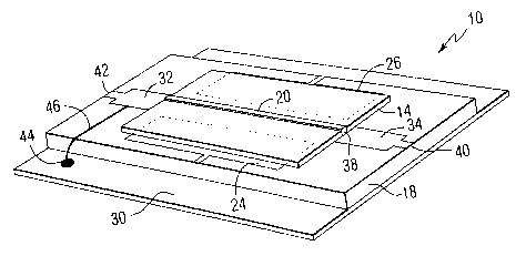
to Referring to the drawings, FIG. 1 is a top plan view of a two port phase
shifter 10 constructed in accordance with the present invention. FIG. 2 is a
cross-
sectional view of the phase shifter of FIG. 1, taken along line 2-2. FIG. 3 is
an isometric
view of the phase shifter of FIG. 1. The phase shifter 10 includes a composite
substrate
12 comprising a first dielectric material layer 14 positioned adjacent to a
surface 16 of a
second dielectric layer 18. The first dielectric layer is comprised of a
voltage tunable
material. The second dielectric layer can be a low loss, conventional non-
tunable
dielectric layer such as aluminum oxide or magnesium oxide, or it could be a
tunable
dielectric layer, which can be the same material as the first dielectric
layer. A microstrip
line 20, preferably made of copper, is positioned on a surface 22 of the first
tunable
2o dielectric layer, on a side opposite that of the second dielectric layer.
First and second
biasing electrodes 24 and 26 are inserted between the first and second
dielectric layers
and positioned on opposite sides of the microstrip so as to leave a slot 28
wider than the
microstrip line itself directly under the microstrip line 20. A ground plane
30, preferably
made of copper, is positioned adjacent to the second dielectric layer on a
side opposite
that of the first dielectric layer.
Matching networlcs 32 and 34, which could be in the form of microstrip
quarter wave transformers, are supported by the second dielectric layer and
connected to
the microstrip line by steps 36 and 38 at the ends of the first dielectric
layer 14. The
matching networks couple the microstrip line 20 to inputloutput ports 40 and
42. While
3o the matching networks are shown to be mounted on the second dielectric
layer, it should
be understood that they could also be mounted on a third dielectric layer (not
shown),
that would in turn be mounted on a second ground plane (not shown). The
matching
networks are electrically coimected to the microstrip line 20. If the
microstrip line is not
CA 02405115 2002-10-04
WO 01/84661 PCT/USO1/14165
6
DC connected to the ground plane via a DC electric path outside the physical
domain of
the phase shifter, such as via a microstrip to waveguide adapter, then one of
the matching
networks should be connected to a DC connection 44 with a radio frequency
block 46 to
ground. The latter could be in the form of a short-circuited quarter
wavelength stub with
a very high characteristic impedance, or a highly inductive wire (RF choke)
connecting
the circuit to the ground plane. The biasing electrodes are supplied with a DC
bias
voltage from an external voltage source 48 via DC feed lines 50 and 52.
The matching networles ensure that a guided wave entering one port 40
(arbitrarily defined as the input port) will enter the phase shifter and heave
it at the other
port 42 (output port), with minimum residual reflections at each port. The
microstrip and
ground plane are kept at zero voltage, while a bias voltage is applied to the
electrodes.
The voltage bias subjects the voltage tunable dielectric material to a DC
electric field,
which affects the dielectric permittivity of the material. In this way, the
dielectric
permittivity of the voltage tunable dielectric material can be controlled by
the bias
voltage. Since the velocity of the guided wave travelling through the device
is inversely
proportional to the square root of the effective dielectric permittivity of
the material
around the strip, the biasing voltage can be used to control the guided wave
velocity.
Therefore it also controls the amount of phase delay at the output port when
referenced
to the input port.
2o The embodiment of FIGS. 1-3 is a wideband device. The bandwidth is
only limited by the matchung networks, which were depicted for the sake of
simplicity as
single stage matching transformers. With multi-stage matchW g networks, an
arbitrary
bandwidth up to an octave or more can be achieved. The embodiment of FIGS. 1-3
would require a comparatively long length of microstrip line for a certain
required
amount of phase shift tuning range. This is because of the fact that the
microstrip line
couples to the ground plane via a composite dielectric, with only one of the
layers in the
composite being tuned.
FIG. 4 is a top plan view of another phase shifter 54 constructed in
accordance with the present invention, and FIG. 5 is a cross-sectional view of
the phase
shifter of FIG. 4, taken along line 5-5. The phase shifter 54 includes a
composite
substrate 56 comprising a first dielectric material layer 58 positioned
adjacent to a
surface 60 of a second dielectric layer 62. The first dielectric layer 58 is
comprised of a
voltage tunable material. The second dielectric layer 62 can be a low loss,
conventional
CA 02405115 2002-10-04
WO 01/84661 PCT/USO1/14165
7
non-tunable dielectric layer such as aluminum oxide or magnesium oxide. A
microstrip
line 64, preferably made of copper, is positioned on a surface 66 of the first
tunable
dielectric layer, on a side opposite that of the second dielectric layer. A
biasing electrode
68 is inserted between the first and second dielectric layers and positioned
directly under
the rnicrostrip line to form a "floating" ground plane for the microstrip
line. A ground
plane 70, preferably made of copper, is positioned adjacent to the second
dielectric layer
on a side opposite that of the first dielectric layer. To avoid resonance
modes in the
floating ground plane/biasing electrode 68, it should preferably be an odd
multiple of
quarter wavelengths long in terms of waves trapped between it and ground plane
70.
l0 Matching networks 72 and 74, which could be in the form of microstrip
quarter wave transfonliers, are supported by the second dielectric Layer and
connected to
the microstrip line by steps 76 and 78 at the ends of the first dielectric
layer. The
matching networlcs couple the microstrip line 64 to inputloutput ports 80 and
82. While
the matching networlcs are shown to be mounted on the second dielectric layer,
it should
be understood that they could also be mounted on a third dielectric layer (not
shown),
that is in turn mounted on a second ground plane (not shown). The matching
networks
are electrically connected to the microstrip. If the microstrip line is not DC
connected to
the ground plane via a DC electric path outside the physical domain of the
phase shifter,
such as via a microstrip to waveguide adapter, then one of the matching
networks should
be connected to a DC coimection 84 with a radio frequency block 86 to ground.
The
latter could be in the form of a short-circuited quarter wavelength stub with
a very high
characteristic impedance, or a highly inductive wire (RF choke) connecting the
circuit to
the ground plane. The biasing electrode is supplied with a DC bias voltage
from an
external DC source 88 via a DC feed line 90.
The embodiment of FIGS. 4-5 is a narrow band device. The bandwidth is
limited to an arbitrary range below or between two of the resonance mode
frequencies of
the floating ground plane. This embodiment requires a comparatively short
length of
microstrip line for a certain required amount of phase shift tuning range.
This is because
of the fact that the microstrip line couples to the floating ground plane only
via a single
3o tunable dielectric layer.
The tunable dielectric used in the preferred embodiments of phase shifters
of this invention has a lower dielectric constant than conventional tunable
materials. The
dielectric constant can be changed by 20 % to 70 % at 20 V/~,m, and typically
by about
CA 02405115 2002-10-04
WO 01/84661 PCT/USO1/14165
8
50 %. The magnitude of the maximum required bias voltage varies with the
distance
between then microstrip and the biasing electrode(s), and typically ranges
from about 8
to 10 V per p.m. Lower bias voltage levels have many benefits, however, the
required
bias voltage is dependent on the device structure and materials. The phase
shifter in the
present invention is designed to have a 360° phase shift. The
dielectric constant can
range from 70 to 600, and typically ranges from 70 to 150. In the preferred
embodiment,
the tunable dielectric is a barium strontium titanate (BST) based film having
a dielectric
constant of about 100 at zero bias voltage. The preferred material will
exhibit high
tuning and low loss. The preferred embodiments utilize materials with tuning
of around
l0 50 %, and a loss as low as possible, which is typically in the range of
(loss tangent) 0.01
to 0.03 at 24 GHz. More specifically, in the preferred embodiment, the
camposition of
the material is a barium strontium titanate (BaXSrI_XTi03, BSTO, where x is
less than 1),
or BSTO composites with a dielectric constant of 70 to 600, a tuning range
from 20 to 60
%, and a loss tangent of 0.008 to 0.03 at K and Ka bands. Examples of such
BSTO
I5 composites that possess the required performance parameters include, but
are not limited
to: BSTO-MgO, BSTO-MgA12O4, BSTO-CaTi03, BSTO-MgTiO3, BSTO-MgSrZrTi06,
and combinations thereof.
The K and Ka band microstrip phase shifters of the preferred
embodiments of this invention are fabricated on a bulk tunable dielectric
layer with a
2o dielectric constant (permittivity) ~ of around 70 to 150 at zero bias and a
thickness of 100
to 150 Vim. The tunable dielectric layer is attached to a low dielectric
constant substrate
Mg0 with thiclmess of about 0.25 mm. For the purposes of this description a
low
dielectric constant is less than 25. Mg0 has a dielectric constant of about
10. However,
the low dielectric substrate can be of other materials, such as LaAl03,
sapphire, A1z03 or
25 other ceramics.
The preferred embodiments of the present invention provide microstrip
phase shifters, which include a tunable permittivity, low loss, bulk BST-based
composite
substrate.
Alternative electronically tunable ceramic material compositions can
3o comprise at least one electronically tunable dielectric phase, such as
barium strontium
titanate, in combination with at least two additional metal oxide phases.
Barium
strontium titanate of the formula BaXSrI_XTi03 is a preferred electronically
tunable
dielectric material due to its favorable tuning characteristics, low Curie
temperatures and
CA 02405115 2002-10-04
WO 01/84661 PCT/USO1/14165
9
low microwave loss properties. In the formula BaXSrI_XTi03, x can be any value
from 0
to l, and preferably from about 0.15 to about 0.6. More preferably, x is from
0.3 to 0.6.
Other electronically tunable dielectric materials may be used partially or
entirely in place of barium strontium titanate. An example is BaXCaI_XTi03,
where x can
vary from about 0.2 to about 0.8, and preferably from about 0.4 to about 0.6.
Additional
electronically tunable ferroelectrics include PbXZrI_XTi03 (PZT) where x
ranges from
about 0.05 to about 0.4, lead lanthanum zirconium titanate (PLZT), lead
titanate
(PbTi03), barium calcium zirconium titanate (BaCaZrTi03), sodium nitrate
(NaNO3),
KNb03, LiNb03, LiTa03, PbNb20~, PbTa20~, KSr(NbO3) and NaBa2(Nb03)5 KH~P04.
to The phase shifter can also include electronically tunable materials having
at least one metal silicate phase. The metal silicates may include metals from
Group 2A
of the Periodic Table, i.e., Be, Mg, Ca, Sr, Ba and Ra, preferably Mg, Ca, Sr
and Ba.
Preferred metal silicates include Mg2Si04, CaSi03, BaSi03 and SrSiO3. In
addition to
Group 2A metals, the present metal silicates may include metals from Group 1A,
i.e., Li,
Na, K, Rb, Cs and Fr, preferably Li, Na and K. For example, such metal
silicates may
include sodium silicates such as NazSi03 and NaSi03-5H20, and lithium-
containing
silicates such as LiAISiO4, Li2Si03 and Li4Si04. Metals from Groups 3A, 4A and
some
transition metals of the Periodic Table may also be suitable constituents of
the metal
silicate phase. Additional metal silicates may include AIZSi20~, ZrSi04,
KA1Si308,
NaAISi308, CaAl2Siz0g, CaMgSi20~, BaTiSi30~ and Zn2Si04. Tunable dielectric
materials identified as ParascanTM materials, are available from Paratelc
Microwave, Inc.
The above tmlable materials can be tuned at room temperature by controlling
the electric
field that is applied across the material.
In addition to the electronically tunable dielectric phase, the present
electronically tunable materials can further include at least two additional
metal oxide
phases. The additional metal oxides may include metals from Group 2A of the
Periodic
Table, i.e., Mg, Ca, Sr, Ba, Be and Ra, preferably Mg, Ca, Sr and Ba. The
additional
metal oxides may also include metals from Group 1A, i.e., Li, Na, K, Rb, Cs
and Fr,
preferably Li, Na and K. Metals from other Groups of the Periodic Table may
also be
suitable constituents of the metal oxide phases. For example, refractory
metals such as
Ti, V, Cr, Mn, Zr, Nb, Mo, Hf, Ta and W may be used. Furthermore, metals such
as Al,
Si, Sn, Pb and Bi may be used. In addition, the metal oxide phases may
comprise rare
earth metals such as Sc, Y, La, Ce, Pr, Nd and the life.
CA 02405115 2002-10-04
WO 01/84661 PCT/USO1/14165
The additional metal oxides may include, for example, zirconnates,
silicates, titanates, aluminates, stannates, niobates, tantalates and rare
earth oxides.
Preferred additional metal oxides include MgZSiOø, MgO, CaTi03, MgZrSrTi06,
MgTi03, MgAI204, W03, SnTi04, ZrTi04, CaSi03, CaSn03, CaW04, CaZr03,
5 MgTa20~, MgZr03, MnOa, PbO, Bi203 and La203. Particularly preferred
additional
metal oxides include Mg2Si04, MgO, CaTi03, MgZrSrTi06, MgTiO3, MgA1204,
MgTa20~ and MgZr03.
The additional metal oxide phases are typically present in total amounts of
from about 1 to about 80 weight percent of the material, preferably from about
3 to about
l0 6S weight percent, and more preferably from about S to about 60 weight
percent. In one
embodiment, the additional metal oxides comprise from about 10 to about SO
total
weight percent of the material. The individual amount of each additional metal
oxide
may be adjusted to provide the desired properties. Where two additional metal
oxides
are used, their weight ratios may vary, for example, from about 1:100 to about
100:1,
typically from about 1:10 to about 10:1 or from about 1:S to about 5:1.
Although metal
oxides in total amounts of from 1 to 80 weight percent are typically used,
smaller
additive amounts of from 0.01 to 1 weight percent may be used for some
applications.
In another embodiment, the additional metal oxide phases may include at
least two Mg-containing compounds. In addition to the multiple Mg-containing
2o compounds, the material may optionally include Mg-free compounds, for
example,
oxides of metals selected from Si, Ca, Zr, Ti, Al and/or rare earths. In
another
embodiment, the additional metal oxide phases may include a single Mg-
containing
compound and at least one Mg-free compound, for example, oxides of metals
selected
from Si, Ca, Zr, Ti, A1 and/or rare earths.
The tunability of the tunable dielectric material may be defined as the
dielectric constant of the material with an applied voltage divided by the
dielectric
constant of the material with no applied voltage. Thus, the tunability
percentage may be
defined by the formula:
T=((X-Y)/X)~ 100;
where X is the dielectric constant with no voltage and Y is the dielectric
constant with a
specific applied voltage. High tunability is desirable for many applications.
For
example, in the case of waveguide-based devices, the higher tunability will
allow for
shorter electrical length, which means a lower insertion loss can be achieved
in the
CA 02405115 2002-10-04
WO 01/84661 PCT/USO1/14165
11
overall device. Voltage tunable dielectric materials preferably exhibit a
tunability of at
least about 20 percent at 8V/micron, more preferably at least about 2S percent
at
8V/micron. For example, the voltage tunable dielectric material may exhibit a
tunability
of from about 30 to about 75 percent or higher at 8V/micron.
In accordance with the present invention, the combination of tunable
dielectric materials such as BSTO with additional metal oxides allows the
materials to
have high tunability, low insertion losses and tailorable dielectric
properties, such that
they can be used in microwave frequency applications. The materials
demonstrate
improved properties such as increased tuning, reduced loss tangents,
reasonable
dielectric constants for many microwave applications, stable voltage fatigue
properties,
higher breakdown levels than previous state of the art materials, and improved
sintering
characteristics. A particular advantage of the described materials is that
tuning is
dramatically increased compared with conventional low loss tunable
dielectrics. A
to further advantage is that the materials may be used at room temperature.
The
electronically tunable materials may be provided in several manufacturable
forms such
as bulk ceramics, thick filin dielectrics and thin film dielectrics.
The present invention relates generally to microstrip voltage-tuned phase
shifters that operate at room temperature in the K and Ka bands. The devices
utilize Iow
loss tunable dielectric layers. In the preferred embodiments, the tunable
dielectric layer
is a Barium Strontium Titanate (BST) based composite ceramic, having a
dielectric
constant that can be varied by applying a DC bias voltage and can operate at
room
temperature.
While the invention has been described in terms of what are at present its
preferred embodiments, it will be apparent to those slcilled in the art that
various changes
can be made to the preferred embodiments without departing from the scope of
the
invention, which is defined by the claims. For example, to avoid the metal
steps between
the microstrip Iine and the matching circuits, in each of the embodiments, the
first
dielectric layer supporting the microstrip line could be sunk into the second
dielectric
layer, so as to ensure that the microstrip line is co-planar with the matching
circuits.