Note: Descriptions are shown in the official language in which they were submitted.
CA 02406780 2002-10-03
Case 2047
PV
MIXER FOR DUAL CONVERSION RECEIVER
The present invention concerns a mixer structure used, in particular, in a
dual
conversion receiver. This type of receiver is used in mobile telephony.
The mixer includes a first variable transconductance stage controlled by a
high
frequency carrier signal, and a second stage connected to the first stage
including, in
parallel, first and second switching means respectively controlled by first
and second
phase opposition control signals at a first intermediate frequency, these
first and
second switching means being powered by a substantially equal current supplied
by
polarisation means.
A mixer structure of this type is known in the prior art as shown in Figure 1.
The mixer includes a first transistor T1 operating in an amplifying mode
having its
source connected to earth, its gate controlled by a signal in1 at a given
frequency and
its drain connected to the source of first T2 and second T3 switching mode
transistors.
The control signal of the amplifying mode transistor can be either an external
high
frequency signal RF received by means of an antenna that is not shown, or a
signal
directly delivered by a local oscillator having its own frequency. The first
T2 and
second T3 switching mode transistors receive at their gate phase opposition
control
signals in2 and in2b at an intermediate frequency IF lower than the frequency
of the
control signal of transistor T1 operating in an amplifying mode. Polarisation
means 4
are provided for these transistors T2 and T3 operating in a switching mode, in
the
form of current sources connected to their drain.
The two transistors T2 and T3 operating in a switching mode enable, in
particular, the frequency of the control signal of transistor T1 operating in
an
amplifying mode to be shifted, either by lowering this frequency or by
increasing this
latter. Thus, phase opposition signals out and outb at frequencies RF-IF and
RF+IF
are present at the mixer output, i.e. at the drain of these two transistors T2
and T3. As
the useful signals at output are current signals, a resistor 5 acting as a
current-voltage
converter is provided between the drain of transistors T2 and T3 operating in
a
switching mode.
Such mixers are used in a dual conversion receiver in order to lower the high
frequency of the signal RF received at a baseband frequency . A receiver using
such
mixers is shown in Figure 2. The receiver includes at least an antenna 11
tuned so as
to receive external signals at a given high RF frequency, for example 900 MHz.
A local
oscillator 12 delivers a clock signal at a frequency LO lower than the RF
frequency of
the received external signal, for example 600 MHz. A first output of the local
oscillator
CA 02406780 2002-10-03
-2-
is connected to frequency divider means 13 which enable four-phase signals I,
Ib, Q
and Qb to be obtained at an intermediate frequency IF, for example 300 MHz.
A first conversion stage E1 formed of two mixers 14 and 15, as defined in
Figure 1, enable four-phase signals Ic, Icb, Qc and Qcb, phase shifted at the
RF
frequency of the received external signal, for example 900 MHz, to be obtained
at the
output of said stage E1.
The first mixer 14 receives as control signals for the two switching mode
transistors, defined in Figure 1, phase opposition signals I and Ib at
intermediate
frequency IF (300 MHz) and as a control signal for the amplifying mode
transistor,
~ 0 also described in Figure 1, the clock signal of local oscillator 12 (600
MHz). The
signals Ic and Icb obtained at the output of the mixer are phase opposition
signals
particularly at the frequency LO+IF.
The second mixer 15 receives, as control signals for the two switching mode
transistors, phase opposition signals Q and Qb respectively in phase
quadrature with
control signals I and Ib of mixer 14 and as a control signal for the
amplifying mode
transistor, the clock signal of local oscillator 12.
Thus at the output of the two mixers 14. and 15, four-phase signals Ic, Icb,
Qc
and Qcb are obtained, particularly at the RF frequency but also at frequencies
IF, LO,
LO-IF.
It is important to note that frequency LO of the clock signal of local
oscillator 12
and intermediate frequency IF of the signals at the output of frequency
divider means
13 are chosen such that the addition of these frequencies LO+IF corresponds to
the
RF frequency of the received external signal.
The receiver also includes a second reception and conversion stage E2 also
formed of two mixers 16 and 17 as described in Figure 1.
The third mixer 16 receives, as control signals for the two switching mode
transistors, phase opposition signals Ic and Icb delivered at the output of
mixer 14,
and as a control signal for the amplifying mode transistor, an external RF
high
frequency signal received by antenna 11.
Fourth mixer 17 receives as control signals for the two switching mode
transistors phase opposition signals Qc and Qcb respectively in phase
quadrature with
control signals Ic and Icb of third mixer 16, delivered at the output of
second mixer 15,
and as a control signal for the amplifying mode transistor, the external high
frequency
RF signal received by antenna 11.
Baseband four-phase signals lout, loutb, Qout and Qoutb are delivered at the
output of the switching mode transistors of third and fourth mixers 16 and 17.
Signals
CA 02406780 2002-10-03
-3-
at different frequencies are also delivered at output, for example RF, IF, LO,
RF+LO+IF ...
The major drawback of such a receiver is that it requires the use of four
mixers
14, 15, 16 and 17 to obtain baseband four-phase signals. Each mixer includes
means
4 for polarising the switching mode transistors. Conventionally, these
polarisation
means are current sources. The use of four mixers necessarily involves having
eight
current sources. As this type of receiver is mainly intended for applications
such as
mobile telephony, reduction in current consumption is a fundamental issue. The
receiver shown in Figure 2 consumes too much current, while occupying a
significant
amount of space on the integrated circuit.
One solution that could be envisaged by those skilled in the art would be to
combine a mixer structure as described in Figure 1 differently, to obtain a
dual
conversion receiver using only three mixers. Such a receiver is shown in
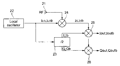
Figure 3.
Like the receiver shown in Figure 2, this receiver includes at least one
antenna
21 tuned so as to receive external signals at a given high RF frequency. A
local
oscillator 22 delivers a clock signal at a frequency LO lower than an RF
frequency of
the signal received by antenna 21. A first output of local oscillator 22 is
connected to
frequency divider means 23 which enable four-phase signals i, Ib, Q, Qb to be
obtained at an intermediate frequency IF.
A first mixer 24 allows the frequency of the external high frequency RF signal
received by antenna 21 to be lowered to intermediate frequency IF. In order to
do this,
mixer 24 receives as control signals for the two switching mode transistors,
described
in Figure 1, phase opposition signals Ilo and Ilob at frequency LO of local
oscillator 22
and, as control signal for the amplifying mode transistor, also described in
Figure 1,
the external signal at a high frequency RF received by antenna 21.
Signals Ic and Icb, frequency shifted, particularly to intermediate frequency
IF,
are delivered at the output of the switching mode transistors of first mixer
24.
Second 25 and third 26 mixers allow frequency IF of the signal Ic obtained at
the output of first mixer 24 to be lowered, in order to obtain baseband four-
phase
signals lout, loutb, Qout and Qoutb.
Second mixer 25 receives as control signals for the two switching mode
transistors, phase opposition signals I and Ib at intermediate frequency IF
supplied at
the output of frequency divider means 23 and as a control signal for the
amplifying
mode transistor, the signal Ic at intermediate frequency IF delivered at the
output of
first mixer 24.
Third mixer 26 receives, as control signals for the two switching mode
transistors, phase opposition signals Q and Qb respectively in phase
quadrature with
CA 02406780 2002-10-03
-4-
control signals I and Ib of second mixer 25, supplied at the output of
frequency divider
means 23 and as a control signal for the amplifying mode transistor, the
signal Ic at
intermediate frequency IF delivered at the output of first mixer 24.
The signals supplied at the output of the receiver are baseband four-phase
signals lout, loutb, Qout and Qoutb.
The current consumption of the receiver according to this solution is also too
high and it occupies too much space on the integrated circuit. Three mixers
are still
necessary and since the control signals of the two mixers 25 and 26 are
provided by
the same mixer 24, the current consumption of mixer 24 is higher than the
normal
consumption of a single conventional mixer.
In order to overcome the drawbacks of the aforementioned prior art, the
invention is characterised in that it concerns a mixer structure allowing the
dual
conversion function to be achieved with greatly reduced power consumption.
The invention thus concerns a mixer as defined in the preamble characterised
in that it further includes means for modulating the first signal delivered by
the first
stage by means of a third control signal at a second intermediate frequency.
The invention also concerns a dual conversion receiver using two mixers
according to the invention.
The invention will now be explained in detail hereinafter for an embodiment
given solely by way of example, this embodiment being illustrated by the
annexed
drawings, in which:
- Figure 1, already described, is a mixer structure according to the prior
art;
- Figure 2, already described, is a dual conversion receiver according to the
prior art;
- Figure 3, already described, is another dual conversion receiver;
- Figure 4 is a mixer structure according to the invention;
- Figure 5 is a dual conversion receiver according to the invention;
The mixer structure, according to the invention, shown in Figure 4, includes
first and second stages similar to those presented in Figure 1.
The first variable transconductance stage A can be formed by a first
transistor
T31 operating in an amplifying mode. This transistor is controlled at its gate
by a high
frequency RF control signal in1, for example 900 MHz, received by an antenna
which
is not shown. Its drain and its source form two terminals, respectively 37 and
38
delivering a useful signal. In this particular mixer structure, this useful
signal is a
current which varies as a function of the control signal in1 received at the
gate of first
amplifying mode transistor T31.
CA 02406780 2002-10-03
-5-
The second stage B connected to terminal 37 of first stage A includes
switching means formed by first T32 and second T33 switching mode transistors.
These first and second switching mode transistors T32 and T33 are respectively
'
controlled at their gate by phase opposition control signals in2 and in2b, at
a first
intermediate frequency iF1, for example 300 MHz. Transistors T32 and T33 are
respectively connected to terminal 37 of first stage A by their source, and
are
respectively powered at their drain by current sources 34 acting as
polarisation means
for these transistors T32 and T33. Preferably, a resistor 5 is placed between
the drain
of these two transistors T32 and T33, resistor 5 acting as a current-voltage
converter.
The current delivered by the two current sources 34 is chosen to be
substantially the same. As control signals in2 and in2b of first and second
switching
mode transistors T32 and T33 are in phase opposition, the current passing
through
said transistors is alternately interrupted at one or other of the two
transistors. The
mean current received at terminal 37 by first amplifying mode transistor T31
is
substantially equal to that delivered by current sources 34. First amplifying
mode
transistor T31 behaves like a variable transconductance and allows a variable
current
to be supplied as a function of control signal in1 received at its gate, to
modulation
means. These means for modulating the current passing through the mixer allow
a
second mixer function to be achieved without increasing the power consumption
of the
initial mixer of Figure 1.
The modulation means are preferably formed by a third transconductance
stage C placed at terminal 38 of first stage A. This third transconductance
stage C
includes a second amplifying mode transistor T36 controlled at its gate by a
control .
signal in3 at a second intermediate frequency IF2. The two terminals of this
third
stage C, namely the source and the drain of second amplifying mode transistor
T36,
are connected respectively to a reference potential Vss and to terminal 38 of
first
stage A.
The purpose of using such a mixer structure according to Figure 4, is to lower
the RF frequency of carrier signal in1, containing the useful signal, received
at the
gate of transistor T31 of first stage A at a baseband frequency in order to be
able to
recover this useful signal.
At terminal 38, the signal supplied is at the same frequency IF2 as that of
control signal in3 of third stage C, namely at the second intermediate
frequency. The
first mixer function is achieved at first stage A via transistor T31, which
allows the
frequency of control signal in1 to be shifted and, in particular, to lower it
to frequency
RF-IF2, at terminal 37. Signals at frequencies RF, IF2, RF+IF2 are also
present at
terminal 37. Pass-band filtering means, which are not shown, around frequency
CA 02406780 2002-10-03
-6-
RF-IF2 can be provided between first stage A and second stage B in order to
keep
only the useful signal at the desired lower frequency, i.e. for example 300
MHz.
The second mixer function is achieved at second stage B by means of the two
transistors T32 and T33 which allow the frequency of the useful signal
received at
terminal 37 to be lowered, to a baseband frequency, RF-IF2-IF1, at the output
terminals out and outb. The signals obtained at these output terminals out and
outb
are in phase opposition. Other signals at different frequencies, for example
RF, IF2,
IF1, RF+IF2+IF1, are also present at these two output terminals. Low-pass
filtering
means, not shown, can be provided at the output of the mixer in order to keep
only the
useful baseband signals.
In this mixer structure example, the signals recovered at output terminals out
and outb are current signals, which is why a current-voltage converter is
preferably
placed at one output in order to convert the recovered signals into voltage
signals.
This current-voltage converter is achieved for example by adding a resistor 5
between
the two output terminals out and outb of the mixer.
It is nonetheless possible to envisage a dual conversion mixer according to
the
invention allowing voltage signals to be recovered directly at output
terminals or even
using the current signals recovered without converting them.
Figure 5 shows a dual conversion mixer utilising two mixers according to
Figure 4.
Like the receiver shown in Figure 2, this receiver includes at least one
antenna
41 tuned so as to receive external signals at a given high RF frequency. A
local
oscillator 42 delivers a clock signal at a natural frequency IF2 lower than
the RF signal
received by antenna 41. A first output of the local oscillator is connected to
frequency
divider means 43 which allow four-phase signals (in2, in2b, in2q and in2qb) to
be
obtained at an intermediate frequency IF1 dependent on the natural frequency
IF2 of
local oscillator 42, for example a ratio of two, then the natural frequency
IF2 of the
local oscillator being two times higher than intermediate frequency IF1.
The receiver also includes two mixers 44 and 45 according to the invention
allowing baseband four-phase signals lout, loutb, Qout and Qoutb to be
delivered at
their outputs.
First mixer 44 receives the clock signal delivered by local oscillator 42 as a
control signal for its first stage, phase opposition signals in2 and in2b at
intermediate
frequency IF1 as control signals for its second stage, and the RF carrier
signal
delivered by the antenna as control signal for its third stage.
Second mixer receives the clock signal delivered by local oscillator as a
control
signal for its first stage, phase opposition signals in2q and in2qb
respectively in phase
CA 02406780 2002-10-03
-7-
quadrature with signals in2 and in2b at intermediate frequency IF1 as control
signals
for its second stage, and the RF carrier signal delivered by the antenna as
control
signal for its third stage. .
As described in Figure 4, each mixer performs dual mixing with the current
consumption of a single mixer. Thus, the receiver's current consumption is
greatly
reduced.
The receiver according to the invention is capable of operating in all the
mobile
telephony frequency bands, for example 1.8 GHz, the frequency of the local
oscillator
and the number of stages of the frequency divider means having only to be
adapted.
It is clear that the description is given only by way of example and that
other
embodiments, in particular of the dual conversion receiver, can form the
subject of the
present invention.