Language selection

Search

Patent 2407533 Summary

Third-party information liability

Some of the information on this Web page has been provided by external sources. The Government of Canada is not responsible for the accuracy, reliability or currency of the information supplied by external sources. Users wishing to rely upon this information should consult directly with the source of the information. Content provided by external sources is not subject to official languages, privacy and accessibility requirements.

Claims and Abstract availability

Any discrepancies in the text and image of the Claims and Abstract are due to differing posting times. Text of the Claims and Abstract are posted:

  • At the time the application is open to public inspection;
  • At the time of issue of the patent (grant).
(12) Patent: (11) CA 2407533
(54) English Title: OPTICAL TELEMETER
(54) French Title: TELEMETRE OPTIQUE
Status: Term Expired - Post Grant Beyond Limit
Bibliographic Data
(51) International Patent Classification (IPC):
  • G01S 07/481 (2006.01)
  • G01S 17/06 (2006.01)
  • G02B 27/09 (2006.01)
  • G02B 27/30 (2006.01)
(72) Inventors :
  • GACHTER, BERNHARD (Switzerland)
  • SCHILLING, ANDREAS (Switzerland)
  • STAUFFER, LAURENT (Switzerland)
  • VOKINGER, URS (Switzerland)
(73) Owners :
  • LEICA GEOSYSTEMS AG
(71) Applicants :
  • LEICA GEOSYSTEMS AG (Switzerland)
(74) Agent: GOWLING WLG (CANADA) LLP
(74) Associate agent:
(45) Issued: 2008-08-05
(86) PCT Filing Date: 2001-02-28
(87) Open to Public Inspection: 2001-11-08
Examination requested: 2005-01-27
Availability of licence: N/A
Dedicated to the Public: N/A
(25) Language of filing: English

Patent Cooperation Treaty (PCT): Yes
(86) PCT Filing Number: PCT/EP2001/002204
(87) International Publication Number: EP2001002204
(85) National Entry: 2002-10-25

(30) Application Priority Data:
Application No. Country/Territory Date
00108836.8 (European Patent Office (EPO)) 2000-04-26

Abstracts

English Abstract


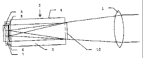
In order to improve target illumination, a light source (2) of an emitter,
which has a laser
diode (3) configured as an edge emitter with a wavelength of 1'550 nm, has
beam
forming optics (4) mounted downstream in relation thereto, which comprise a
cylindrical
lens (7) and a first deflection element (8) with three fields having different
diffraction
structures. Said deflection element deflects partial beams exiting from
successive
segments of the emission edge to three fields of a second deflection element
(10) which
are located next to one another and crosswise in relation to the first fields
and which also
have different diffraction structures. Said deflection element directs the
partial beams to
the aperture of a collimator (1) in such a way that the partial beams
substantially fill said
aperture. The first deflection element (8) and a mount (6) for the cylindrical
lens (7) are
integral and, alike the second deflection element (10), are made of plastic.
Both parts are
glued to opposite sides of the frontal areas of a block (5) made of glass.


French Abstract

Afin d'améliorer l'éclairage cible, une source lumineuse (2) d'un émetteur comportant une diode laser (3) d'une longueur d'onde de 1 550 nm sous forme d'élément à émission par la tranche, présente un dispositif optique de formation de faisceau placé en aval (4), qui comprend une lentille cylindrique (7) ainsi qu'un premier élément de déviation (8) dont les champs possèdent trois structures de diffraction différentes. Cet élément de déviation diffracte des faisceaux partiels, à partir de sections successives de la tranche d'émission, sur des champs d'un second élément de déviation ayant trois structures de diffraction différentes juxtaposées et perpendiculaires aux premiers champs, les faisceaux partiels étant orientés vers l'ouverture d'un collimateur (1) pratiquement rempli par lesdits faisceaux. Le premier élément de déviation (8) et un support (6) pour la lentille cylindrique (7) sont formés d'un seul tenant et sont en matière plastique, tout comme le deuxième élément de déviation (10). Les deux pièces sont collées sur des surfaces de contact opposées d'un bloc (5) en verre.

Claims

Note: Claims are shown in the official language in which they were submitted.


7
What is claimed is:
1. Optical telemeter target illumination apparatus, comprising:
at least one light source for target illumination, and
a collimator collimating radiation emitted by said light source prior to
target illumination,
said light source being arranged in front of said collimator,
said light source comprising at least one laser diode having an emission edge,
said emission edge including successive segments,
said light source having beam forming optics mounted downstream of said at
least one laser
diode for illuminating said collimator,
said light source generating offset partial beams,
wherein said offset partial beams are emitted from the successive segments of
the
emission edge of the at least one laser diode,
the offset partial beams being parallel to the emission edge and overlapping,
said beam forming optics comprising a first deflection element based on
diffraction or refraction
of light and a second deflection element based on diffraction or refraction of
light, each of said
first and second deflection elements having plane surfaces divided into at
least two fields.
2. Optical telemeter target illumination apparatus according to claim 1
wherein said at least one
laser diode emits with a wavelength between 850 nm and 980 nm.
3. Optical telemeter target illumination apparatus according to claim 1
wherein said at least one
laser diode emits with a wavelength of approximately 1,550 nm.
4. Optical telemeter target illumination apparatus according to claim 1
wherein said beam
forming optics comprise a cylindrical lens immediately following after said at
least one laser
diode, said cylindrical lens having an axis that is parallel to the emission
edge of said at least one
laser diode.
5. Optical telemeter target illumination apparatus according to claim 4
wherein the diameter of
said cylindrical lens is less than or equal to 65 µ.

8
6. Optical telemeter target illumination apparatus according to claim 4
wherein the distance
between the emission edge and said cylindrical lens is less than or equal to
15 µ.
7. Optical telemeter target illumination apparatus according to claim 1
wherein said first
deflection element deflects the partial beams in different ways in a direction
transverse to the
emission edge and also in a direction parallel to the emission edge,
wherein the partial beams strike the second deflection element substantially
side by side,
the second deflection element orienting the partial beams as beams originating
from a line in a
focal plane of the collimator.
8. Optical telemeter target illumination apparatus according to claim 7,
wherein the fields of each of said first and second deflection elements are
oriented
parallel to the emission edge and contain different diffraction structures,
and
wherein the number of fields of the second deflection element corresponds to
the
number of fields of said first deflection element, the fields of the second
deflection element
containing different diffraction structures.
9. Optical telemeter target illumination apparatus according to claim 7,
wherein said beam forming optics comprise a block of transparent material with
a first
front face to which said first deflection element is fastened and an opposite
second front face to
which said second deflection element is fastened.
10. Optical telemeter target illumination apparatus according to claim 7,
wherein said first
deflection element and the said second deflection element are made of a
plastic.
11. Optical telemeter target illumination apparatus according to claim 9
wherein said cylindrical
lens is tied to a mount fastened to the first front face of said block.
12. Optical telemeter target illumination apparatus according to claim 11
wherein said first
deflection element is integral with said mount.

9
13. Optical telemeter target illumination apparatus according to claim 11
wherein said at least
one laser diode is fastened to said block by soldering.
14. Optical telemeter target illumination apparatus according to claim 4
wherein said cylindrical
lens is fastened to said at least one laser diode with cement.
15. Optical telemeter target illumination apparatus according to claim 1
wherein said beam
forming optics is designed to superimpose the partial beams in a far field.
16. Optical telemeter target illumination apparatus according to claim 1
wherein said beam
forming optics is designed for imaging the partial beams in the far field onto
a nearly square
field.

Description

Note: Descriptions are shown in the official language in which they were submitted.


11, UKI. ZUU1 14:40 UU413 3yy1U49
IVtt, ylb4 ~, Lb/4U
CA 02407533 2002-10-25
WO 01/54077 1 PCT/EP 01/02204
DESCRIPTION
OPTICAL TELEMETER
Technical field
The invention relates to an optical telemeter such as employed for instance in
the surveying
of piots of land and buildings.
Prior art
Optical telemeters of this kind have been known for somc timc alrcady. The
lascr diodcs
used as light sources have the disad.vantage, however, that the light beam
exiting at the
emission edge has a very long and narrow cross section. This lcads to poor
target
illumination, since only parn of the light beam strikes the target thus
detracting from the
range and from measuring accuracy. Moreover, reflection of parts of the beam
missing the
target at other objects, which for instance are more distant, may acutely
disturb the
mcasurcrnents,
Aescrfiptlon of the invention
The iztvenxion is based on the task to specify an optical telemeter of the
above kind
providing a better target illumination than known tclcmctcrs of this kind_
The advantages attained by the invention chiefly reside in a decisive
improvement of
range, i.e., the maximum distance that can be measured or, for a given range,
in an
increased rrteasuring accuracy.
Brief description of the drawings
zn the following, the invention is described in greater detail with the aid of
figures
representing mcrcly one embod7snent.

11, UK I, 1UV1 14: 4U UU4'Lj jyy I U4y Ivh(, y I b4 ~, (y/4U
CA 02407533 2002-10-25
WO 01/84077 2 PCT/EP 01102204
Figure 1a schematically shows a lateral view of an emitter of a telemeter
according to the
invention.
Figure 1b schematically shows a top view of the emitter according to Figure I
a,
Figure 3 shows a top view in bearxi direction of a first deflection element of
the emitter
according to Figures 1 a, b,
Figure 4 shows a top view counter to the beam direction of a second deflection
element of
the emitter according to Figures 1 a, b, and
Figure 5 shows the target ill **-+*+Ation attained by the emitter according to
Figures 1a, b.
Ways to practice the invention
An optical telemeter according to the invention comprises an emitter as well
as a receiver
tkaat, in known manncr. can for instancc be built up with optics and avalanche
photodiodes,
and further cormprises an electronic control and evaluating unit also of known
design
controlling the emission of light pulses by the emitter and evaluating the
output signal of
the receiver. The distan,ce can be measured by transit-time deterznina.txon or
by the phasc-
xnatching technique.
The emitter has a collimator 1 and a light source 2 put in front of it which
is composed of a
laser diode 3 and beam forming optics 4. The laser diode 3 is an edge emitter
emitting
electromagnetic waves in the infrared, preferably at a wavelength between 850
nm and 980
nm or a wavelength % = 1,550 z1um. The emai,ssion edge has a Iength between 30
m and g00
m while its width is between 1 zn and 3 m. The emission edge may bc
intcrruptcd in its
lomgiltudinal direction. For im.stance, instead of one laser diode 3 a linear
array of laser
diodes having edge lengths of for instance 50 .m and distanccs bctw-ccn
succcssive edges
of 100 m could be provided. The numerical aperture corresponding to the sine
of half the
angular aperture has a valuc of 0.1 parallel to the emission cdge and of 0.6
to 0.7 transverse

21. UKI. 1UU1 14;4U 0041j jyylU4y irR. y io(+ 0. )viI+u
CA 02407533 2002-10-25
WO 01/84077 3 PCT/EP 01/02204
to this edge. The product of these two quantities, knowrx as space bandwith
product (SBP),
in a direction transverse to the emission edge approximately corresponds to
the wave-
lcngth, and thus is practically monomodal (transverse nnodo of 0), i.c_, it is
closc to a
fundamental limiting value that cannot be exceeded, while parallel to the
emission edge it
is larger than this limiting valuc by a factor of 10 to 100. Even in this
dixectilon. the 5BP
cannot be altered by conventional refracting elements such as lenses, but with
the aid of
elements based on diffraction or refraction of light, it can be lowered very
close to the
emission edge by rearrangement in a direction parallel to the emission edge
but instead be
enhanced in a direction tzazasvexse to ihis edge, and thus the light beam can
be more
strongly collimated.
This xs the purposc of the bcam forming optics 4 con-iprising a
parallclcpipcdal block 5
consistiaag of a transparent material, preferably glass, with a first front
face turned toward
the ].ascr diodc 3 and an opposite second front face turned toward the
eollimator 1_ The grst
front face supports a mount 6 of plastic holding a cylindrical lens 7 at its
terminal zones.
The cylindrical lens 7 has a czzculax cross section, its diameter is about 60
xn_ It is oriented
parallel to the emission edge of laser diode 3 and spaced apart from tlus
diode by about 10
l.tm, The beam exiting from the emission edge which for laser diodes of the
kind employed
has a large transverse radiation angle of about 80 is madc parallel by it.
The diameter of
the cylindrical lens and its distance from the emission edge may also be much
larger than
the given values, but for small valucs, particularly for values of at most 65
tn and at most
15 zn, respectively, the overlap of the -fractions coherently radiated from
successive
rcgions of the edge is very small so that the losses caused by this overlap
are also kept low.
Downstream of the cylindrical lens 7 a~iurst detXection element S is arranged
which is
integral with the mount 6 and has a structured surface that is essentially
plane and parallel
to the first front face of block 5. Parallel to the emission edge it is
divided into three
successi,vc fZclds 9a, b, c having different steppcd diffraction structures.
The second,
opposite front face of block 5 suppports a second deflection element 10
consisting of
plastic and comprising a structurcd surface essentially plane and psrallel to
the second
front face that is divided into three successive fields 11 a, b, c transverse
to the emission
edge also having different stepped ditf~eaction struetures.

21, OKT, 2002 14;40 00413 j991049 iN K. y 10 4
CA 02407533 2002-10-25
WO 01/84077 4 PCT/EP 01l02204
The upper field 9a of the first deflection element 8 has a structuee such that
it deflects the
partial bcam cxiting from an uppcr scgmcnt of the emission odgc and striking
it to the lcft-
hand field 11a (looking in beam direction) of the second deflection element 10
where the
beazn is insignificantly deflected so that it will strike the collimator 1 and
approximately
fill the left-hand third of the collimator's aperture. In exactly
corresponding manner, the
lower field 9c of the first deflection element 8 deflects the paztial beam
exiting from a
lower segment of the exnassion edge and striking it, to the right-hand field
11c (looking in
beam direction) of the second deflection element 10, where this beam, too, is
deflected
precisely in the corresponding way and then fills approximately the right-hand
third of thc
aperture of collimator 1. The central third of the collimator is filled by the
partial beam
exiting from a slightly shorter central segnent of the emission edge and
passing without
deflection through the unstxuctured central fields 9b and 11b of the first
deflection element
8 and second deflection clement 10, zespectively.
'T'hus, the three partial beams are so deflected in different ways by the
first deflection
element 8 that they strike the second deflection element 10 side by side (when
looking in a
direction tzansverse to the emission edge), hence their projections onto a
plane formed by
thc dircctions of the exnission edge and of the bcam csscntially coincide. In
the second
de#Xection element 10 they are then so deflected in different ways that they
strike the
collimator 1 as if they all came from a line parallel to the emission edge in
the focal plane
of collimator 1 or, stated differently, in such a way that their back
extrapolation will lead to
such a line, and tbat each partial beam fills approximately one third of the
aperrture of
collimator 1. The three successive segments of the emission edge are imagcd
onto a ncarly
square field, and indeed in such a way that they are superimposed in the far
field (Figure
5). This secures an excellent target illumination.
At wavelengths between 850 mzza a.xid 950 nm the beam can be collimated very
strongly,
allowing a range scan with high lateral resolution. Wavelengths around 1,550
nm are also
very advantageous, since then the upper limit of the admissible single-pulse
energy which
is defined in terms of safety to the eyes has a value of about 8 mJ and thus
is higher by a
facto,t of about 16,000 than at wavelengths between 630 and 980 nm. By
employing this

11, UKI. 1UUZ 14;4U UU4'Lj jyylU4y IVtt. ylb4 5. ~L/4U
CA 02407533 2002-10-25
'= WO 01/84077 5 PCT/EP 01/02204
factor at least in part, which becomes possible because of better beam
concentration
according to the invention, one can very substantially increase the range or,
for a given
range, raise the sensitivity.
The mount 6 and the first deflection element 8 that is integral with it, as
well as the second
deflection element 10, each are produced by one of the replication techniques
as described
in M. T. Gale, 'Replication', in H. P. Herzig (editor), 'Micro-Optics', Taylor
& Francis
1997, pp. 153-177, for instance by etching of a cylinder or piston of quartz
and by hot
ombossing, injcction molding, or casting followed by UV curing, and are then
bonded to
block 5. The defuntion of the diffraction structures can be performed with
known computer
programs. The rcplication tecbnique allows large numbers of parts to be
fabricated at
favorable cost. Since the mount 6 is also made by this teehnique, a very
precise positioning
of cylindrical lens 7 is possible. The tolerated va,riation of distance
between the lens and
the first defleotion element 8 is a fcw micrometers. Using soldering and
active adjustment
as described i.zx DE-A- 197 51352, the laser diode 3 can then be bonded in
such a way to
the beam forming optics 4 that the tolerated variation of mounting between it
and the
cylindrical lens 7 is about 0.5 zn.
Various modifications of the embodiment described are possible. Thus, the
cylindrical lens
may bc fastened with cement directly to the laser diode. The first deflection
element and
the second deflection element may also consist of glass, and for instance be
madc by an
etching process. They may also be etched directly into the block separating
them. The
number of fields in the deflection elements may be two, four or morc, instcad
of three. The
beam forming optics may consist of refracting elements, for instance prisms
and plates.
Finally, laser diodes having wravelengt.hs particularly between 600 nm and
1,000 nm, arnd
more particularly between 630 nm and 980 zum which are outside the regions
indicated
above can be cmploycd.
List of reference symbols
1 Collimator
2 Light source

11, UKI, 2UU1 14.41 UU42j jyy IU4y iyrc. y 104 0. 7)/4u
' CA 02407533 2002-10-25
WO 01/84077 6 PCT/EP 01/02204
3 Laser diode
4 Beam forming optics
Block
6 Mount
5 7 Cylindricallerxs
8 first deflection element
9a,b,c Fields
second deflection element
11 ab,c Fields

Representative Drawing
A single figure which represents the drawing illustrating the invention.
Administrative Status

2024-08-01:As part of the Next Generation Patents (NGP) transition, the Canadian Patents Database (CPD) now contains a more detailed Event History, which replicates the Event Log of our new back-office solution.

Please note that "Inactive:" events refers to events no longer in use in our new back-office solution.

For a clearer understanding of the status of the application/patent presented on this page, the site Disclaimer , as well as the definitions for Patent , Event History , Maintenance Fee  and Payment History  should be consulted.

Event History

Description Date
Inactive: Expired (new Act pat) 2021-03-01
Common Representative Appointed 2019-10-30
Change of Address or Method of Correspondence Request Received 2018-01-10
Inactive: S.8 Act correction requested 2008-10-10
Inactive: Prior art correction 2008-10-03
Inactive: Acknowledgment of s.8 Act correction 2008-10-03
Inactive: Cover page published 2008-10-03
Inactive: S.8 Act correction requested 2008-08-19
Grant by Issuance 2008-08-05
Inactive: Cover page published 2008-08-04
Pre-grant 2008-05-21
Inactive: Final fee received 2008-05-21
Notice of Allowance is Issued 2008-03-06
Letter Sent 2008-03-06
Notice of Allowance is Issued 2008-03-06
Inactive: First IPC assigned 2008-02-29
Inactive: IPC assigned 2008-02-29
Inactive: IPC removed 2008-02-29
Inactive: IPC assigned 2008-02-29
Inactive: Approved for allowance (AFA) 2007-12-21
Amendment Received - Voluntary Amendment 2007-08-13
Inactive: S.30(2) Rules - Examiner requisition 2007-02-26
Inactive: S.29 Rules - Examiner requisition 2007-02-26
Inactive: IPC from MCD 2006-03-12
Letter Sent 2005-02-02
Request for Examination Received 2005-01-27
Request for Examination Requirements Determined Compliant 2005-01-27
All Requirements for Examination Determined Compliant 2005-01-27
Letter Sent 2003-04-16
Inactive: Single transfer 2003-02-25
Inactive: Courtesy letter - Evidence 2003-02-04
Inactive: Cover page published 2003-02-04
Inactive: Notice - National entry - No RFE 2003-01-31
Application Received - PCT 2002-11-27
National Entry Requirements Determined Compliant 2002-10-25
Application Published (Open to Public Inspection) 2001-11-08

Abandonment History

There is no abandonment history.

Maintenance Fee

The last payment was received on 2008-01-23

Note : If the full payment has not been received on or before the date indicated, a further fee may be required which may be one of the following

  • the reinstatement fee;
  • the late payment fee; or
  • additional fee to reverse deemed expiry.

Patent fees are adjusted on the 1st of January every year. The amounts above are the current amounts if received by December 31 of the current year.
Please refer to the CIPO Patent Fees web page to see all current fee amounts.

Owners on Record

Note: Records showing the ownership history in alphabetical order.

Current Owners on Record
LEICA GEOSYSTEMS AG
Past Owners on Record
ANDREAS SCHILLING
BERNHARD GACHTER
LAURENT STAUFFER
URS VOKINGER
Past Owners that do not appear in the "Owners on Record" listing will appear in other documentation within the application.
Documents

To view selected files, please enter reCAPTCHA code :


To view images, click a link in the Document Description column. To download the documents, select one or more checkboxes in the first column and then click the "Download Selected in PDF format (Zip Archive)" or the "Download Selected as Single PDF" button.

List of published and non-published patent-specific documents on the CPD .

If you have any difficulty accessing content, you can call the Client Service Centre at 1-866-997-1936 or send them an e-mail at CIPO Client Service Centre.


Document
Description 
Date
(yyyy-mm-dd) 
Number of pages   Size of Image (KB) 
Representative drawing 2002-10-24 1 6
Abstract 2002-10-24 1 28
Claims 2002-10-24 3 114
Drawings 2002-10-24 1 33
Description 2002-10-24 6 265
Claims 2007-08-12 3 107
Abstract 2008-03-05 1 28
Representative drawing 2008-07-23 1 7
Reminder of maintenance fee due 2003-02-02 1 106
Notice of National Entry 2003-01-30 1 189
Courtesy - Certificate of registration (related document(s)) 2003-04-15 1 107
Acknowledgement of Request for Examination 2005-02-01 1 176
Commissioner's Notice - Application Found Allowable 2008-03-05 1 164
PCT 2002-10-24 15 669
PCT 2002-10-25 7 324
Correspondence 2003-01-30 1 23
Fees 2003-01-16 1 35
Correspondence 2008-05-20 2 48
Correspondence 2008-08-18 1 30
Correspondence 2008-10-09 1 38
Correspondence 2008-11-19 1 8